1. Introduction
Active-matrix organic light-emitting diode (AMOLED) displays have been widely applied from mobile devices such as smart-phone to wearable devices such as smart-watch and smart-band, owing to its advantages of being light weight and thin, and having a low-voltage drive, self-illumination, and fast response speed [
1,
2]. In mobile devices using AMOLED displays, low power usage is one of the most important performance requirements. In particular, the recent development of the low temperature polycrystalline oxide (LTPO) process significantly reduces the driving current of AMOLED displays, and mobile devices are equipped with always on display (AOD) functions, making it essential to have high power efficiency even under light loads.
Both a positive and negative power are required to operate an AMOLED panel, which are generally supplied by a two-channel DC-DC converter using a V
POS channel that generates positive power and a V
NEG channel that generates negative power [
3].
There are two main ways to configure a two-channel DC-DC converter. One is a method consisting of two independently regulated DC-DC converters with a boost converter and an inverting buck-boost converter that are integrated into a single chip [
4,
5]. This method has relatively good ripple and high power efficiency, but has the disadvantages of bulky size and high cost due to the use of two inductors. The other is a method using a single-inductor bipolar-output (SIBO) type [
6,
7,
8]. This method shrinks the device size and lowers the cost, but if each output load current of the SIBO converter is the same as the load current of the conventional converter, the output ripple will be larger than that of a conventional converter. In this study, we will focus on the design of a high-performance DC-DC converter with high power efficiency and low ripple for mobile displays using the former method.
As the positive voltage V
POS with a fixed voltage causes a change in the current flowing through an organic light-emitting diode (OLED) device to affect its brightness, a small ripple is required for the change in output current and input voltage. In particular, current fluctuation owing to periodic transmission is introduced in wireless communication devices; this fluctuation appears as a flicker defect that can be recognized by the human eye. Therefore, a V
POS design with a low ripple for input voltage fluctuation is required [
9,
10].
By contrast, the negative voltage V
NEG generates a voltage with a large variable range for screen brightness control; a high-voltage power transistor is used to withstand the voltage stress of the switching node. Occurrence of large switching losses, especially under light loads, contributes to the requirement for a design that can reduce the same. Moreover, as V
NEG comprises a circuit with a wide output range, it is difficult to optimize the design for changes in driving conditions, such as input voltage and output current, device characteristics, and operating temperature. Therefore, power loss due to dead-time occurs easily [
11,
12], and an adaptive dead-time control circuit is required to maintain a constant dead-time in response to changes in driving conditions.
Various studies have been conducted to reduce switching losses in order to improve efficiency under all loads, including light loads [
4,
13,
14,
15,
16,
17]. A pulse width modulation–pulse skip modulation (PWM–PSM) dual-mode method [
4,
14] or a pulse width modulation–pulse frequency modulation (PWM–PFM) dual-mode method [
5,
15,
16] that operates using PWM under heavy loads, and PSM or PFM under light loads have been proposed. However, as the PWM–PSM dual-mode method omits switching pulses arbitrarily, the ripple in output voltage is large, making it difficult to use AMOLED panels where output quality is highly demanded. The PWM–PFM dual-mode method includes its own set of disadvantages, in which the hardware area becomes large owing to the independent configuration of the circuits required for each mode, and the preparation time are additionally required for mode switching, resulting in a high ripple.
In this paper, we designed a two-channel high-performance DC-DC converter that outputs a positive voltage V
POS with a small ripple for the variation in input voltage and a negative voltage V
NEG with high power efficiency, in order to be applicable to a mobile AMOLED display under light loads of 100 mA or less. The V
POS was designed as a boost converter topology using a novel input voltage variation reduction circuit (IVVRC) to have a low ripple. The V
NEG was designed as an inverting buck–boost converter topology using both the pulse width modulation–set time variable pulse width modulation (PWM–SPWM) dual-mode method [
18] and an adaptive dead-time using voltage detection of switching node (ADTVS) control method to increase power efficiency.
This paper is structured as follows:
Section 2 details the design of the proposed two-channel high-performance DC-DC converter for AMOLED display;
Section 3 presents the measurement results of an implemented chip; and
Section 4 discusses the conclusion.
2. Two-Channel High-Performance DC-DC Converter Design for AMOLED Display
In this section, we discuss the design of the proposed two-channel high-performance DC-DC converter consisting of a VPOS boost converter that outputs a positive voltage with a small ripple, and an inverting buck–boost converter that outputs a negative voltage VNEG with high power efficiency, such that it can be applied to mobile AMOLED displays.
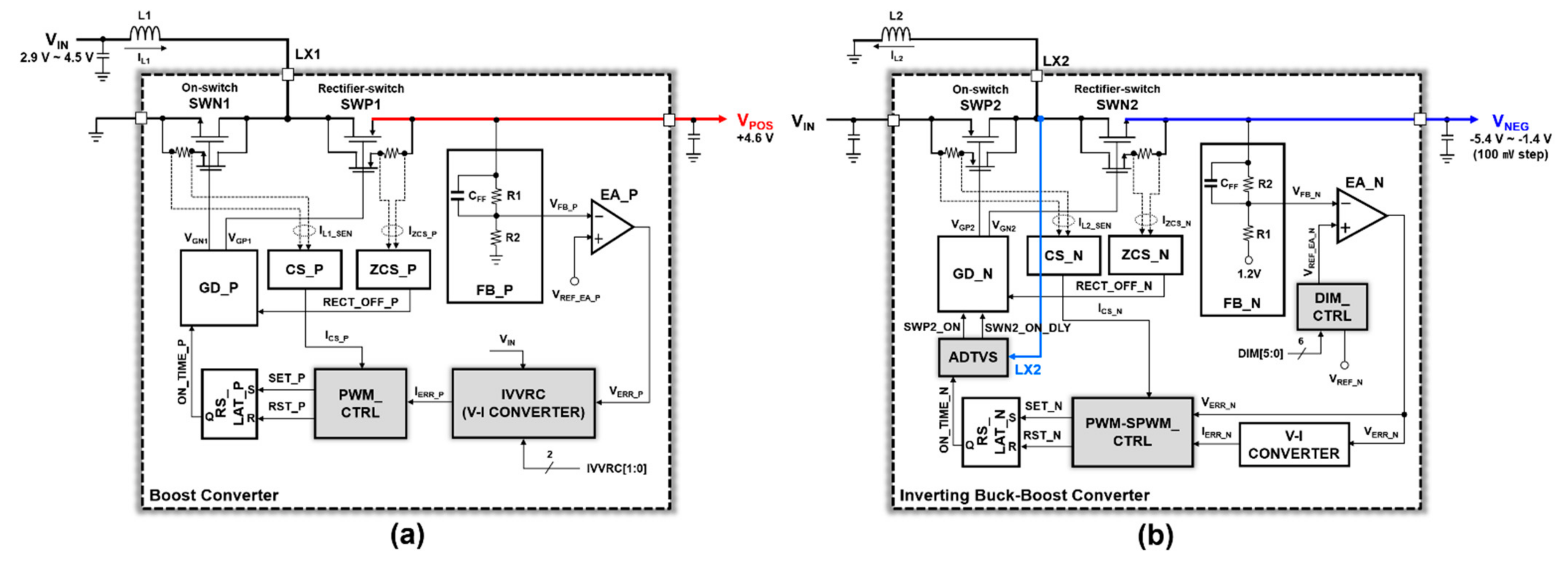
Figure 1 shows a block diagram of the proposed two-channel high-performance DC-DC converter for AMOLED displays. The V
POS of
Figure 1a was designed as a boost converter to obtain a fixed positive 4.6 V output, for an input voltage V
IN of 2.9 V to 4.5 V. We propose an IVVRC to reduce overshoot and undershoot for large variations in input voltage V
IN, and utilized PWM single-mode switching to reduce the ripple for output current fluctuations. By contrast, the V
NEG shown in
Figure 1b was designed as an inverting buck–boost converter to obtain an output voltage of −5.4 V to −1.4 V, for an input voltage V
IN of 2.9 V to 4.5 V. To improve the power efficiency, the PWM–SPWM dual-mode method was used to reduce the switching loss, thereby resulting in a switching at a frequency proportional to the output current at light loads [
18]. An ADTVS circuit was proposed to reduce power loss in the dead-time interval, by maintaining a constant dead-time against changes in driving conditions.
2.1. VPOS for a Low Ripple
In this subsection, we propose an IVVRC that has a small output ripple for input voltage fluctuations to minimize flickering in mobile AMOLED displays. We then design a VPOS boost converter using the described circuit.
2.1.1. Proposed IVVRC
IVVRC is a circuit that reduces overshoot and undershoot of output voltage by rapidly changing the pulse width using a circuit which feeds forward current corresponding to the input voltage fluctuations occurring during the transmission and reception in wireless communication devices.
Figure 2 shows the proposed IVVRC that converts the output voltage V
ERR_P of the error amplifier into the current I
ERR_C, using the V-I converter-I, and feeds the current of the I
VIN_C2 corresponding to the input voltage V
IN to the output current I
ERR_P to reduce the amount of change in I
ERR_C. That is, it reduced time to change to the final output current I
EER_P, thus reducing the overshoot and undershoot ripple of the output voltage V
POS.
Figure 3 shows the timing diagram of the IVVRC with increasing input voltage V
IN. When the input voltage increases (
Figure 3a), the error current I
ERR_P and the on-time decreases (
Figure 3b,d). Further, the amount of change in the current I
ERR_P and I
ERR_C based on the change in the input voltage V
IN became smaller by I
VIN_C2 (
Figure 3c). Consequently, I
ERR_P with IVVRC responded quickly to input voltage V
IN changes, thereby reducing the overshoot of V
POS (
Figure 3e).
2.1.2. VPOS Circuit Design
Figure 1a shows a block diagram of a boost converter that generates a positive voltage V
POS.
Switching frequency and duty of the boost converter using the PWM single mode are controlled by a PWM controller (PWM_CTRL). The switching frequency is controlled by a set-pulse (SET_P) generated by the PWM_CTRL with a fixed frequency of 1.5 MHz. The duty is controlled by a reset pulse (RST_P) when the peak current (ICS_P) of the inductor increases and becomes equal to the error current (IERR_P) of the output voltage (VPOS) during on-time when the power transistor SWN1 is turned on.
Using the IVVRC proposed in
Section 2.1.1, the error current responded quickly to abrupt changes in the input voltage (V
IN) to reduce the ripple of the output voltage.
If a reverse current occurs through SWP1 during off-time when the power transistor SWP1 is turned on, ZCS_P detects and blocks it to eliminate power loss.
A detailed circuit of the PWM_CTRL of V
POS is shown in
Figure 4.
The switching operation having a constant frequency was performed by the set pulse generating circuit SET_P, as shown in
Figure 4a; the duty was controlled by the reset pulse generating circuit RST_P, as shown in
Figure 4b. In the SET_P generation circuit, an RST signal or a SET signal became “high” by charging and discharging through a current source I
OSC and a capacitor C
OSC, such that a set-pulse with a frequency of 1.5 MHz was generated. The RST_P generation circuit shown in
Figure 4b output a pulse signal of RST_P indicating the end of on-time, when the peak current I
CS_P of the inductor reached the error current I
ERR_P of the error amplifier.
Figure 5 shows the timing diagrams of the PWM mode boost converter. Regardless of the increase in the output current I
OUT in
Figure 5a, SET_P has a clock operation with a frequency of 1.5 MHz (
Figure 5b). During on-time, when the sensing current I
CS_P of the inductor node became equal to I
ERR_N (
Figure 5c), RST_P output “high” (
Figure 5d).
Figure 5e is a timing diagram of the switching node LX1, and
Figure 5f shows the waveform of the current I
L1 flowing through the inductor. Under light loads, the on-time was short, whereas the off-time was long. Hence, the current flowing through the SWP1 power transistor into the V
POS during off-time, flowed backward. In this case, the ZCS circuit detected a reverse current to prevent unnecessary conduction.
2.2. VNEG for High Power-Efficiency
In this subsection, a PWM–SPWM dual-mode method is presented; it was used in order to reduce the switching loss under light loads [
18]. Additionally, an ADTVS control circuit was proposed to reduce the power loss caused by the dead-time in heavy loads. We also designed a V
NEG as an inverting buck–boost converter topology for high power efficiency, using these two circuits.
2.2.1. PWM–SPWM Dual-Mode Switching Method
Under heavy loads, PWM–SPWM dual mode operates in PWM mode; this controls the duty at a fixed switching frequency. Under light loads, the dual mode operates in SPWM mode to reduce switching loss, which controls the frequency of the set signal for switching power transistors in proportion to output current using a voltage-controlled oscillator (VCO).
Figure 6 shows the switching frequency based on the output current of the PWM–SPWM dual mode switching method. For heavy loads greater than the mode change current I
MC, the method operates in PWM mode with a fixed switching frequency; however, in the case of light loads smaller than I
MC, it operates in SPWM mode with variable frequency. Additionally, the dual mode method can change the frequency of the VCO output signal based on the output current; hence, it is possible to change the I
MC for switching between the PWM mode and SPWM mode.
As the method operated like a PFM that changed the switching frequency in proportion to the output current under light loads, the switching loss was reduced and improved power efficiency was obtained. The method only adds a VCO and a clock selection circuit for varying the frequency of the set pulse based on the PWM mode, thereby reducing the overhead of the circuit configuration in the dual mode. The PWM-based circuit has a structure in which only the set pulse is variable through the VCO; this allows it to respond without delay while changing modes. It is also fairly simple to change the SPWM operation range considering the power efficiency and the output voltage ripple, based on the resolution and size of the display panel by changing the mode conversion output current.
2.2.2. Proposed ADTVS Circuit
An ADTVS is a circuit for dead-time control that optimizes power loss in a dead-time interval, transitioning from on-time to off-time, by detecting the fall time of the switching node and further maintaining a constant dead-time irrespective of the changes in driving conditions.
Figure 7 shows the proposed ADTVS circuit and timing diagrams of the circuit. The LX2_LEVEL_SENSOR circuit outputs PULSE “1”, when the VGN2 signal is “high” and the switching node LX2 voltage is still “high” at the point when the on-time ends and the off-time begins. This further delays the rising start time of VGN2 in the next cycle through the DELAY_COUNTER and the SWN_ON_DELAY. By contrast, if the LX2 voltage is “low,” the LX2_LEVEL_SENSOR outputs PULSE “0”, and then speeds up the rising start time of VGN2 in the next cycle. This adaptive control maintains the constant dead-time even when the fall time of the switching node voltage is changed in driving conditions, thereby preventing an increase in power loss due to changes in dead-time.
2.2.3. VNEG Circuit Design
Figure 1b shows a circuit block diagram of an inverting buck–boost converter that generates a negative voltage V
NEG.
A circuit for the PWM–SPWM dual-mode method that was discussed in
Section 2.2.1 was embedded using a PWM–SPWM dual-mode controller (PWM-SPWM_CTRL) to reduce the switching loss. The ADTVS circuit discussed in
Section 2.2.2 was used to prevent power loss occurring in dead-time interval, by keeping dead-time constant against changes in driving conditions. The ZCS_N block detected reverse current that may occur through SWN2 during off-time, when the power transistor SWN2 was turned on. It further blocked the reverse current to eliminate power loss. Both the CS_N block and the ZCS_N block used shunt resistors to sense current; the size of the switching transistor for current sensing was designed to be 1/100th the size of the power transistor to reduce the loss caused by resistance.
Figure 8 shows a PWM–SPWM dual-mode controller circuit that controls the switching frequency and the duty of the dual mode, in detail. The set-pulse (SET_N) that controls the switching frequency was generated by a set-pulse generator circuit shown in
Figure 8a, and the reset-pulse (RST_N) that determines whether a duty was generated by a reset-pulse generator circuit shown in
Figure 8b.
When the output current changed, the frequency of VCO_SET was changed by the VCO. The LOW_FREQ_SEL selected a signal with a lower frequency, between the PWM_SET signal with a constant frequency of 1.5 MHz and the VCO_SET signal that outputs the VCO, and outputs it as a SET signal. Under light loads, the VCO_SET signal lower than the PWM_SET signal of 1.5 MHz was selected, and under heavy loads, the PWM_SET signal of 1.5 MHz was selected. The generation circuit of reset pulse RST_N shown in
Figure 8b is the same in the SPWM mode or the PWM mode. The RST_N generated when the output current IERR_N of the error-amplifier and the inductor current ICS_N sensed during on-time obtained the same value.
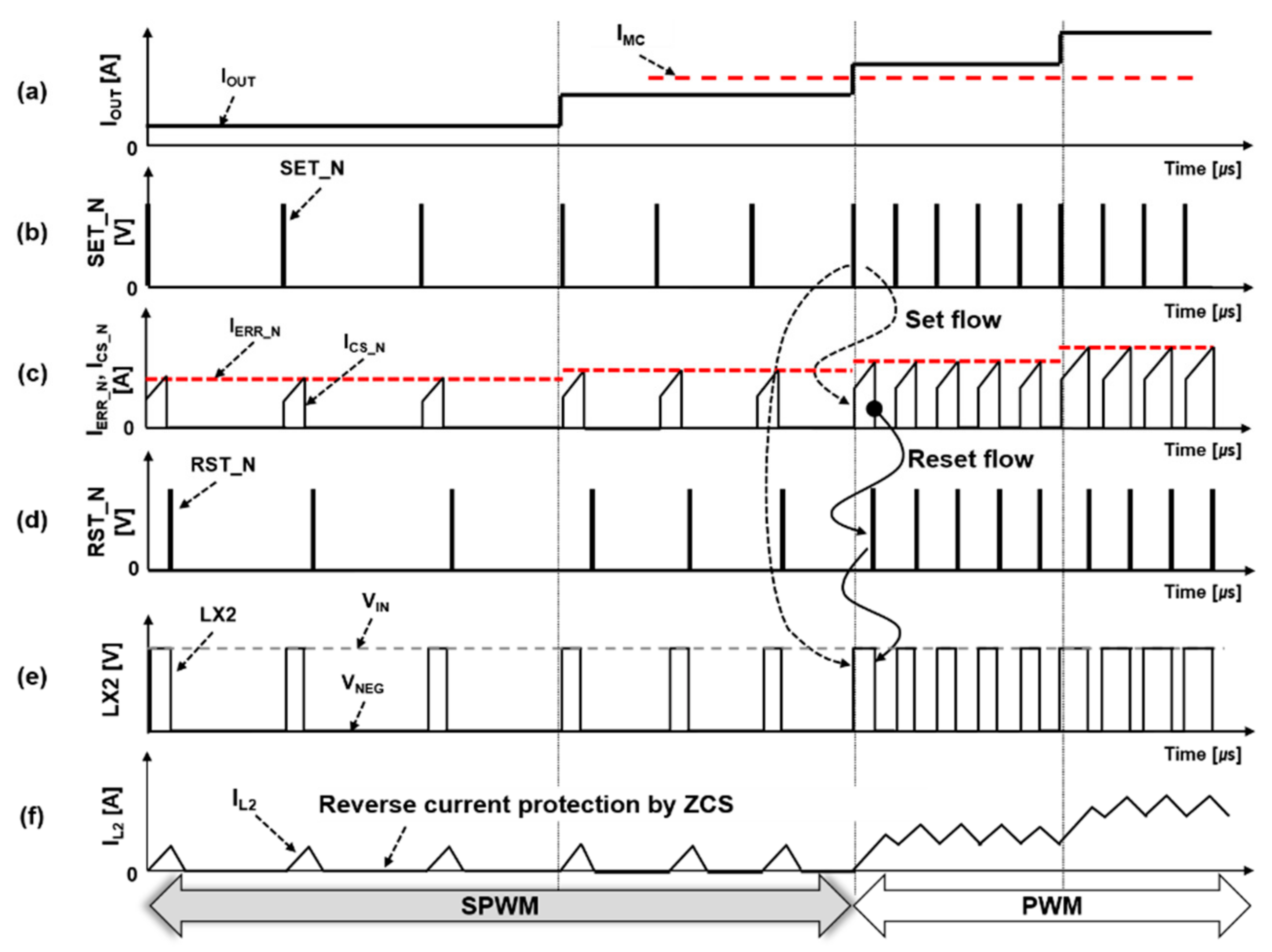
Figure 9 shows the timing diagrams based on the output current of the proposed PWM–SPWM dual-mode inverting buck–boost converter. When the output current I
OUT was less than the mode switching current I
MC (
Figure 9a), the frequency of the SET_N increased in proportion to the output current (
Figure 9b). However, when the output current was greater than the I
MC (
Figure 9a), the frequency of the SET_N was fixed at 1.5 MHz. During on-time when the sensing current I
CS_N of the inductor node became equal to I
ERR_N (
Figure 9c), RST_N was generated.
Figure 9e shows the voltage waveform of the switching node LX2, where the range of the LX2 voltage moves from V
IN to V
NEG. Additionally,
Figure 9f shows the current I
L2 waveform flowing through the inductor. During off-time, the current flowing from V
NEG to the LX2 flowed back through rectification switching SWN2; hence, ZCS_N in
Figure 1b outputs a RECT_OFF_N signal, and the GD_N turned off the power transistor SWN2 when the RECT_OFF_N became “high”.
Figure 10 shows the performance simulation results of the V
NEG inverting buck–boost converter that employs the ADTVS circuit. The dead-time t
DF based on the output currents for with and without ADTVS circuit is shown in
Figure 10a. When the output current was increased from 0 mA to 300 mA, t
DF increased from 5 ns to 9.5 ns without the ADTVS circuit; however, with the ADTVS circuit, t
DF was maintained with a lower delay-time of 1 ns to 2 ns.
Figure 10b shows the simulation results of power efficiency. With the application of the ADTVS circuit, power efficiency increased by about 0.8% under heavy loads of an output current of 50 mA, or more in PWM mode operation; the maximum efficiency of the inverting buck–boost converter at an output current of 100 mA was 90.6%.
3. Experimental Results
The proposed two-channel DC-DC converter was implemented using a 0.35 μm BCD process.
Figure 11 shows a chip micrograph with an area of 1.67 mm × 2.44 mm.
Table 1 shows the results of the performance measurements of our proposed two-channel DC-DC converter, and other methods for AMOLED displays. The range of the input voltage was 2.9 V to 4.5 V, whereas the output voltage was V
POS = 4.6 V, and V
NEG = −1.4 V to −5.4 V, where the maximum output current was 300 mA. Electrical characteristic data were measured at V
IN = 3.7 V, V
POS = 4.6 V, and V
NEG = −4.0 V, and the efficiency was measured at I
MC = 50 mA.
Figure 12 shows the waveforms of the input voltage and the output voltage of V
POS at the output current of 100 mA, while changing the input voltage of the assumed RF noise from 4.2 V to 3.7 V, periodically. Without IVVRC, the overshoot of V
POS was 9.9 mV, and the duration time was 34 μs, whereas the undershoot of V
POS was 9.8 mV, and the duration time was 34 μs. However, with IVVRC, the undershoot and overshoot of the V
POS were reduced to 4.5 mV and 3.2 mV, respectively. This resulted in a significant reduction in the ripple of the output voltage, to 45.5% and 32.7%, respectively, for variation in the input voltage, due to the use of IVVRC.
Figure 13 shows the measurement results of the output voltage ripple of the two-channel DC-DC converter. At a light load of output current of 5 mA, the ripple of the output V
POS using the PWM single mode was 3.0 mV, whereas the ripple of the output V
NEG using the PWM–SPWM dual mode was 5.5 mV. In the case of [
4] that uses PSM, the ripple of the V
NEG was 7.1 mV. Therefore, our SPWM mode scheme showed smaller results. This has been attributed to the regular generation of switching clocks in the SPWM mode, as compared to the large number of switching clocks being omitted in the PSM mode.
Figure 14 shows the load transient waveforms. For load transient measurements, the ripple and the duration time of V
POS and V
NEG were measured when the output current was changed from 0 mA to 60 mA with a slope of 5 μs, and back to 0 mA. For the proposed V
NEG using PWM–SPWM dual mode, the overshoot was 21 mV and the duration time was 14 μs, as shown in
Figure 14a. In case of the V
NEG using PWM–PSM dual mode in [
4], the overshoot was 24 mV and the duration time was 24 μs, as shown in
Figure 14b. Therefore, the overshoot of our V
NEG was 3 mV smaller than that of [
4], and the duration time was 10 μs faster than [
4]. This may be the result of the PWM–SPWM dual-mode method that only generated set pulses through VCO, based on PWM and the reset circuit that generated a constant clock of 1.5 MHz operating together, which allowed the mode transition based on the increase in the output current to reach 1.5 MHz in the PWM mode without time delay.
Figure 15 shows the combined power efficiency results of V
POS and V
NEG of our two-channel DC-DC converter. The power efficiency ranged between 72.9% to 90.4%, and when the inverting buck–boost converter of V
NEG was driven in the PWM single mode under light loads, the efficiency ranged between 47.0% to 90.4%. That is, as the inverting buck–boost converter that generates V
NEG operated in the PWM–SPWM dual mode, the switching loss under light loads was reduced, thereby improving the power efficiency by 25.9% under light load of 5 mA, as compared to the PWM single mode with a switching frequency of 1.47 MHz that improved by 13.7% at 10 mA. Under heavy loads of 50 mA or higher, it operated in the PWM mode to obtain a 90.4% power efficiency, which is the same as that obtained in the PWM single mode.
A performance comparison of the proposed converter that uses PWM–SPWM dual mode with conventional converters is presented in
Table 1. Ref. [
4] and [
5] are typical commercial two-channel DC-DC converters consisting of two independent converters, like our converter; [
4] is a converter that uses PWM–PSM dual mode; and [
5] is a converter that uses PWM–PFM dual mode. Additionally, [
6,
7,
8] are two-channel DC-DC converters with a SIBO structure that output two power sources from V
NEG and V
POS with one inductor.
Power efficiency results showed that our two-channel DC-DC converter obtained 72.9%~90.4% at 5 mA~100 mA light load output current, which is 2.7%~5.8% higher than the output of the previous converter [
4], and accounts for the highest power efficiency under light loads of less than 100 mA among the converters listed in
Table 1, except for [
7].
Additionally, the V
NEG ripple obtained a voltage of 5.3 mV in this converter at output currents of 5 mA and 7.1 mV in [
4] using PSM, thus resulting in a 25% smaller ripple performance. This is because the SPWM method obtains a small ripple from performing a constant switching operation with a frequency proportional to the decrease in the output current.
As a consequence, our work shows the highest power efficiency and the smallest ripple of the output voltages at light loads of 100 mA or less among the two-channel DC-DC converters consisting of two independent converters.
Ref. [
7] is very power efficient under light load, but has large ripple with a maximum output current of 30 mA, which is not suitable for mobile devices with a main operating range of 100 mA or less. Generally, though DC-DC converters with a SIBO structure have high power efficiency or a small chip area, they have large output ripple and are improper to apply to mobile device displays.
4. Conclusions
In this paper, we proposed a design of a two-channel high-performance DC-DC converter that provides the output of a positive voltage VPOS with a small ripple and a negative voltage VNEG with high-efficiency, for use in the mobile AMOLED displays. The VPOS employs a boost converter structure, proposes an IVVRC circuit that reduces ripple for input voltage fluctuations, and was designed as a PWM single mode to reduce ripple for output current fluctuations. VNEG uses an inverting buck–boost structure, and applies a PWM–SPWM dual-mode method and an ADTVS circuit that maintains a constant dead-time in order to reduce switching power loss.
In the measurement results of the proposed chip using a 0.35 μm BCD process, the power efficiency was improved by 25.9% compared to PWM single-mode operation at an output current of 5 mA, resulting in 72.9%. Additionally, the maximum power efficiency was 90.4% at an output current of 100 mA. In addition, when the IVVRC circuit was applied, the ripple of V
POS resulted in 4.5 mV, which improved by 55% as compared to the ripple without the IVVRC function, for a 0.5 V input voltage fluctuation. The power efficiency of the proposed converter is 2.7%~5.8% higher than the output of the previous converter [
4] and the output voltage ripple of V
POS and V
NEG at an output current of 5 mA improved by 19% and 25%, respectively, as compared to those of [
4].
The two-channel DC-DC converter for AMOLED display proposed in this paper has high power efficiency and low ripple, and is applied to various mobile devices under light loads of 100 mA or less for mobile AMOLED displays to be able to increase the display driving time and provide high-quality images within a limited battery capacity.


