Abstract
This paper presents the design and implementation of a miniaturized high-voltage power supply with power factor correction (PFC) for atmospheric-pressure plasma jet (APPJ) applications. The sinusoidal output frequency and voltage of the power supply can be controlled independently from 16 to 24 kHz and from 1 to 10 kVpeak, respectively. A helium APPJ load is used to assess the performance of the developed power supply. It is shown that the developed high-voltage power supply operates effectively, and the designed PFC converter improves the input current distortion of the power supply. Not only the power factor of the power supply is increased from 0.41 to 0.95, but it also provides a low-ripple DC voltage, which reduces the high-voltage ripple of the output from 730 to 50 Vp-p. In this paper, the proposed design integrates the PFC converter into the high-voltage power supply so that the developed power supply has better electrical characteristics and the overall power supply can be significantly miniaturized.
1. Introduction
By continually improving the design of plasma generators for decades, the atmospheric-pressure plasma has been compliant with the low-temperature work to ensure safe operations. Among atmospheric-pressure plasma designs, the atmospheric-pressure plasma jet (APPJ) [1,2] is the most commonly used for many applications. The atmospheric-pressure plasma jet produces plasma with a narrow area and high power density, suitable for single-point processing. Therefore, many novel applications related to APPJ can be found in the biomedical field, including root canal disinfection [3], tooth bleaching [4], and treatment of human extremities [5]. Handheld commercial APPJ devices will become popular for biomedical sterilization or surface treatment in the near future. For ease of use during treatment, it is crucial to miniaturize the plasma power supply.
This paper aims to design a miniaturized plasma power supply. The expected output of the designed power supply has a high-voltage AC sinusoidal waveform, the output voltage is adjustable at a fixed frequency, and it has a burst mode feature to protect the plasma generator when the temperature is too high. We propose to improve the conventional design in the commercially available product [6] by changing the autotransformer and high-voltage transformer to improve the disadvantages of having a large volume so that the space for circuit composition is significantly reduced.
This study first introduces the model of the plasma load. In [7,8,9,10,11], the plasma models were simplified as combinations of several capacitors and threshold voltages. Here, we use the model introduced in [12] with the relationships between the structure and capacitors in [11]. The value of the capacitor at a non-discharged state is calculated approximately by measuring the dimensions of the APPJ structure and the arrangement of the ground electrode. The obtained parameters of the model are then used in the simulation. In addition, the high-voltage transformer model [13] and the inverter circuit are also built in the simulation. Based on the simulation-based design, the feasible transformer specifications are determined by simulating the gain curves of the input and output. Finally, the plasma model is combined with the designed high voltage transformer circuit, and the design of the high voltage power supply is validated by the simulation.
There are many advantages in our proposed design over conventional designs. In the design, we redesign the high-voltage transformer to have a higher resonant frequency so that it does not have a drastically changing gain in the operating range; this way we can have advantages such as reduced operating current, inductance value, and coil wire diameter. The heat and Electromagnetic Interference (EMI) issues can also be improved by reducing the transformer’s size. Although this reduces the boost ability of the inverter, the front-end converter can compensate for this reduced capability. Through such a design compromise, we can reduce the volume of the back-end inverter. Furthermore, the external DC power supply is integrated into the designed high-voltage power supply. Most plasma power supplies are based on stand-alone DC power combined with high-voltage power supplies [14,15] or Marx generators [16,17], and are thus bulky and heavy, with limited portability. To overcome these disadvantages, in this study, a flyback PFC converter [14,18] is use to replace the front-end DC power supply. Since the output voltage of a flyback converter is arbitrarily step-up/down, it is different from the boost system that is only used when the output voltage is higher than the input voltage. It is very suitable for miniaturization applications as a front-end circuit. It can not only replace the external DC power supply but also improve the capability of power factor correction [19]. Based on the above two improvements, the overall power supply can be further significantly miniaturized.
For practical applications, we used the helium APPJ as an output load, compared the difference between simulation and experimental results, and validated the effectiveness of the electrical function through measurement data. The performance of APPJ load was assessed by optical emission spectroscopy (OES) [20,21,22]. Finally, in comparison with the case study, the test results show that it is a successful miniature integrated design.
The rest of this paper is organized as follows. Section 2 discusses the structure and equivalent electrical model of a plasma jet. Section 3 describes the design steps of power supply circuits. In Section 4, a description of the experimental setup is given and then the results of simulations and experiments are compared. Section 5 presents the concluding remarks.
2. Equivalent Electric Circuit Model of Plasma Jet
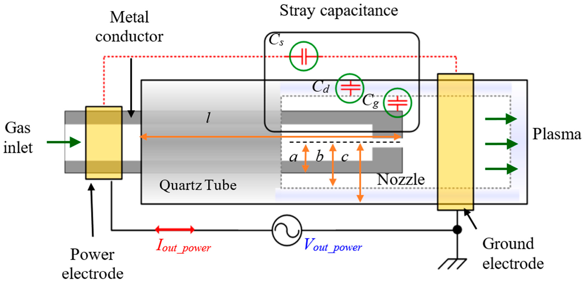
A schematic diagram of an APPJ in this paper is shown in Figure 1. The APPJ consists of a quartz tube, a capillary stainless tube, an aluminum nozzle, and aluminum foil. The quartz tube serves as a dielectric layer.
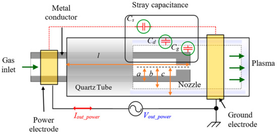
Figure 1.
Schematic diagram of the atmospheric pressure plasma jet.
The powered electrode (capillary stainless tube and aluminum nozzle) is inserted into the quartz tube tightly using polytetrafluoroethylene (PTFE) sealing tape, and aluminum foil is wrapped around the quartz tube as the grounded electrode. The distance between the powered electrode and the grounded electrode is 15 mm. Here, a is the radius of the electrode tube, b and c are the inner and outer radii of the quartz tube, respectively, and l is the length of the powered electrode. At the undischarged state, the equivalent circuit model of the APPJ consists of two capacitors connected in series with capacitances Cg and Cd. As shown in Figure 1, Cg represents the capacitance between the power electrode and dielectric barrier (quartz tube), and Cd represents the capacitance of the wall of the quartz tube. The parallel capacitance Cs represents the stray capacitance from the power supply and connecting wire. However, during the discharge process, Cg must be modified to describe the electrical characteristics. From [7,9,10,11,12], it can be represented by three types, as described below:
The first type [7] uses a voltage-controlled current source model as shown on the right-hand side of Figure 2a. In the figure, Rg is the plasma sheath resistance, and Cg is the gas capacitance. Both parameters vary with the composition of the gas, but the primary discharge current varies according to the value of Vg(t). The current of the voltage-controlled current source is given by
where Vg(t) represents the discharge gas voltage, I0 represents the leakage current at the non-discharge state, and Vth represents the breakdown voltage level. Equation (1) gives that when Vg(t) is greater than Vth, the discharge current rises rapidly.
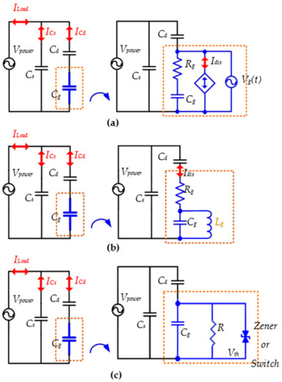
Figure 2.
Equivalent model of a plasma jet: (a) dependent voltage source, (b) LC circuit and (c) TVS component.
The parameter α adjusts the slope of the discharge current . This parameter depends on the plasma load, whose range is typically between 1 and 12. In addition, the total current ILoad(t) of the equivalent model can be obtained by Kirchhoff’s rule, and it is given by
where Vpower(t) represents the input voltage and Vd(t) represents the voltage of Cd. While such a model is accurate, the analysis of this model becomes more complicated.
The second type of model [11] consists of a capacitor Cg, an inductor Lg in parallel, and a series resistor Rg, as shown in Figure 2b. Here Rg represents the conductivity of the current return paths. The model reflects the transient characteristics in the simulation results; when the discharge process occurs, the resistance Rg changes from a high resistance value to a low resistance value, and the high-frequency resonance of the LC circuit represents the vibration of the electron collision in the discharge process. Because the frequency of electron collisions is much higher than the drive frequency, the spiking phenomenon at discharge can appear in the simulation waveform.
The third type of the equivalent model [9,10,12] is shown in Figure 2c. The equivalent circuit of the air dielectric structure is represented by the capacitance Cg, resistance R, and semiconductor components in parallel. Here the values of Cg and R vary with the gas discharge. R represents the energy consumed during discharge, and Vth is the trigger voltage of the component in the discharge state. Triggering of the discharge state can be modeled by a transient surge suppressor (TVS) or power switch. This model assumes that the plasma discharge current rises quickly as long as the applied voltage is greater than the TVS voltage level. The TVS stays at the cut-off condition when the applied voltage is lower than the TVS voltage level.
In this paper, we used the third type model to do the simulation-based design to quickly determine the approximate working range of the system. Since the plasma jet configuration does not use the same material along the entire length in this study, the value of Cg cannot be calculated directly. Instead, we used the approximate method proposed in [11] to calculate the capacitance values of this structure, through assuming that the surfaces defined by the specific radius have the same potentials (boundary conditions). Capacitances of Cd and Cg in the non-discharged state can be obtained by
where is the dielectric constant of vacuum, is the relative dielectric constant of quartz, and is the dielectric constant of air. The parameter Cs can be obtained from the connector specifications or by measuring the connection line.
3. Power Supply System
Before designing the proposed circuit, a case study on a commercially available product PVM500 [6] was conducted. PVM500 is a typical high voltage power supply. It consists of an autotransformer and high-voltage inverter [10,12,13]; the output voltage is adjusted by the autotransformer (AC/AC) on the input side and then converted to a DC voltage via the rectifier. The symmetrical half-bridge is used for the inverter. The squared voltage wave generated by this inverter is used as the input source of a high-voltage transformer, enabling the resonant network to produce a high alternating voltage and repeatedly exciting the plasma. In this case study, we found that the dimension of this power supply was 10 × 17.5 × 25 cm3. The volume of such a power supply has much room for improvement. The autotransformer and the high voltage transformer occupy the most space. If circuits or components with less volume can replace these parts, then the power supply size may be significantly reduced. This paper proposes two points to miniaturize the power supply.
- For the high-voltage transformer: The volume of the high-voltage transformer can be reduced by redesigning the output characteristics of the inverter. By limiting the frequency range and making the frequency range well below the maximum resonance point, the inductance and winding current are reduced so that the size of the transformer can be smaller.
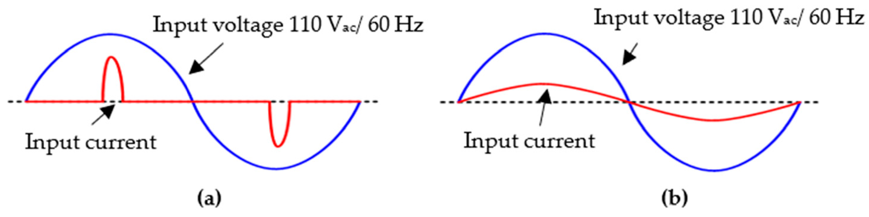
- For the autotransformer: An adjustable AC/DC converter can replace the autotransformer, and the resulting volume can be significantly reduced. The design of PVM500 uses a bridge rectifier with filter capacitors to convert AC to DC; such a rectifier circuit turns the input current into a pulse surge, and the peak value of the current is three to five times larger than the ideal average current, as shown in Figure 3a. This current distortion results in a lower power factor value and decreases the regional power network efficiency and quality. If it can be changed to an active PFC converter to improve the plasma device input current distortion, then the corrected current waveform is illustrated in Figure 3b.
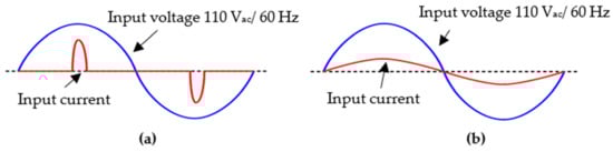 Figure 3. Schematic diagrams of input current distortion: (a) before improvement and (b) ideal improvement.
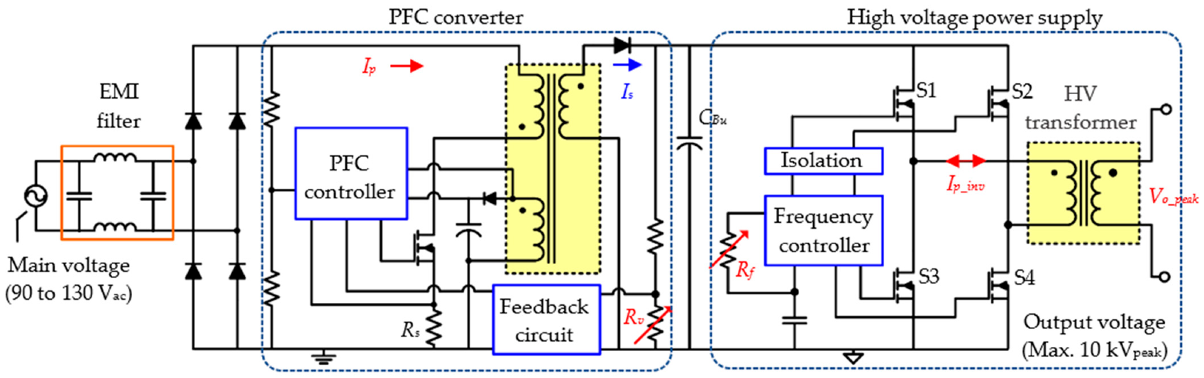
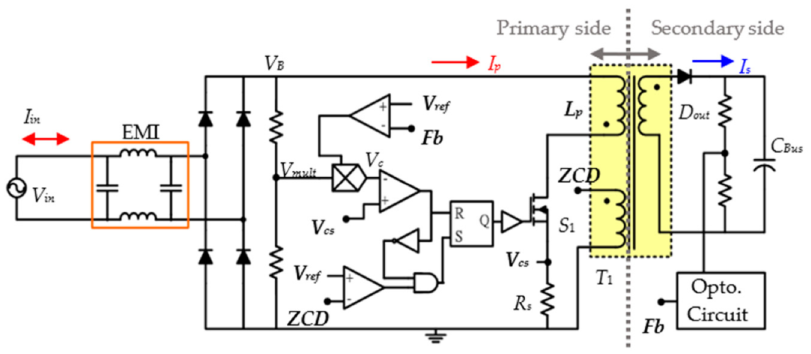
In this paper, the solutions mentioned above are adopted in the design of the power supply. A schematic overview of the proposed power supply circuit is shown in Figure 4, in which the adjustable voltage and frequency can be controlled by resistances Rv and Rf, respectively. In this design, the high-voltage secondary side only has the output voltage sensing, and there are no control and no other feedback circuits. The design of the transformer of the high-voltage power supply and the PFC converter is given below.
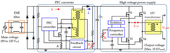
Figure 4.
Circuit of the power supply with PFC controller.
3.1. Transformer of High-Voltage Power Supply
This circuit uses the full-bridge circuit topology to design the inverter because most AC sinusoid power supplies have the transformer output directly connected to the plasma load. Such a circuit has no diodes or synchronous switches on the secondary side to cut off the current loop, and the power stage circuit on the primary side withstands voltage feedback from the secondary side voltage.
When the energy is transferred from the primary side to the secondary side, the parasitic and load capacitance on the secondary side can store the energy. Thus, not all of the electrical energy can be released into the gas load. Especially when the output voltage is lower than the gas discharge threshold, the energy cannot be effectively released. The energy is fed back to the primary side when the voltage changes polarity, and it can be stored in parasitic capacitance on the primary side or returned to the BUS capacitor through the leakage inductance. In this way, different load capacitances can significantly influence this circuit, and it always results in a matching problem between the plasma load and the AC high-voltage power supply. The equivalent capacitance values for different plasma generators may vary significantly. For a transformer with a high turn ratio, the uncertain load capacitance on the secondary side can affect the operating characteristics of the primary-side circuit, so we initially choose a simple topology to avoid circuit failure.
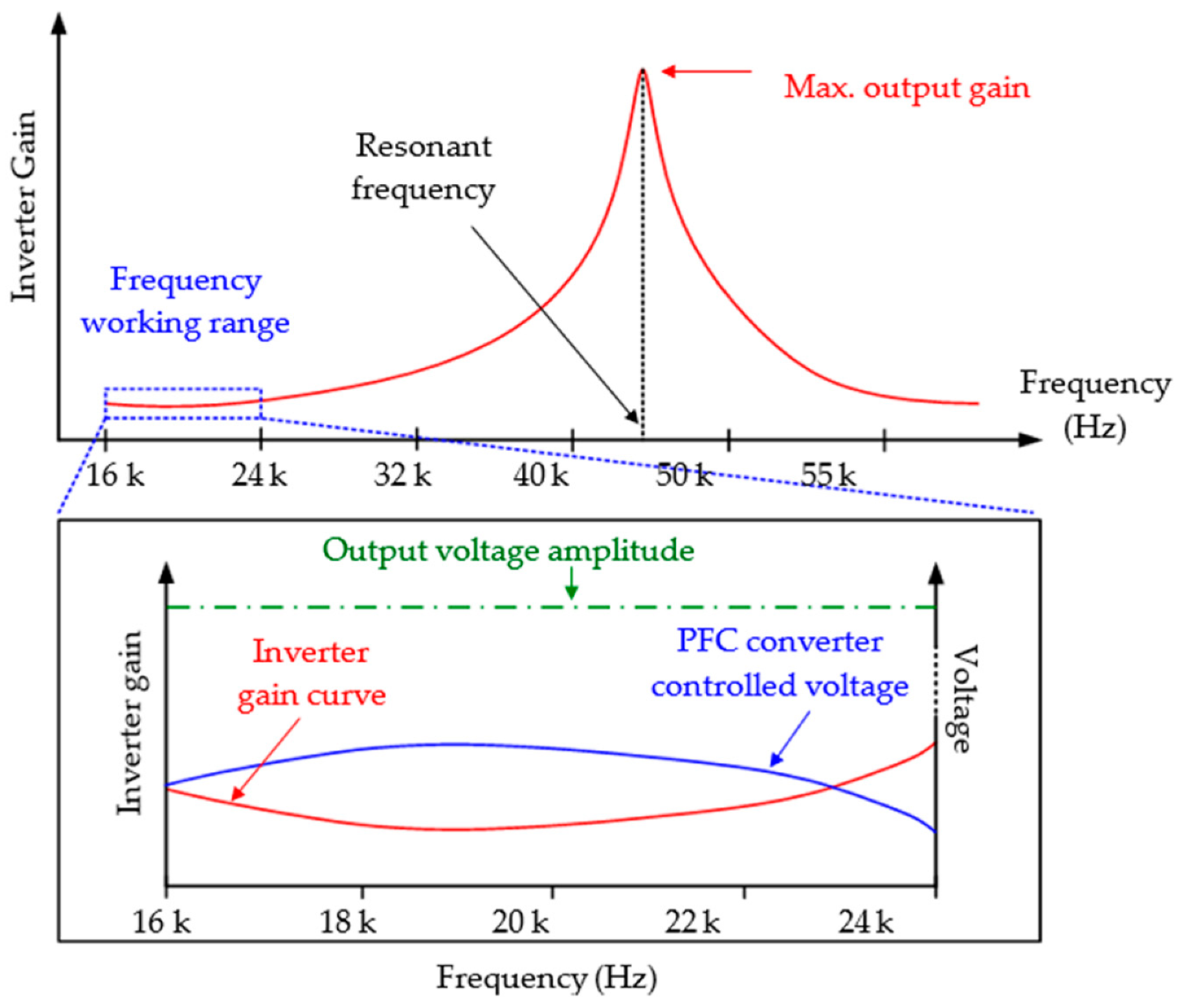
The proposed high-voltage power supply consists of only a transformer and a full-bridge inverter. Thus, the output voltage gain of the power supply entirely depends on the resonant characteristics of the transformer. The operating frequency range is between 16 and 24 kHz in this paper, and we desire the transformer gain curve of the DC voltage (Vdc_Bus) to the AC output peak (Vo_peak) to rise gently in the frequency range, rather than operating near the rapidly varying resonant frequency point, as shown in Figure 5.

Figure 5.
Output voltage gain of the inverter.
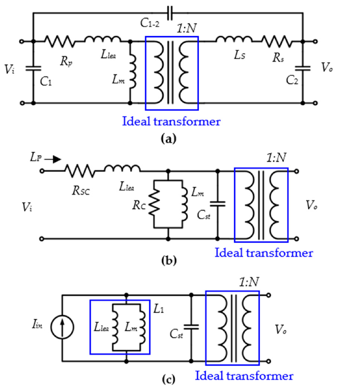
This design can reduce the resonance current such that the transformer size can be reduced. Assuming that the orange line at the bottom of Figure 5 is the gain curve of the transformer, and the blue line is the DC voltage (Vdc_Bus) controlled by the PFC converter from the previous stage, the gain variation of the transformer is compensated to achieve regulation of the output voltage amplitude (as illustrated by the green dashed line). The design of the transformer with the desired resonance characteristic curve is the primary concern here. Considering the transformer equivalent circuit in [15], the typical equivalent model of a transformer is shown in Figure 6a. The model includes an ideal transformer (with turns ratio N), primary side inductance LP, magnetizing inductance Lm, leakage inductance Llea, secondary-side inductance LS, winding resistances (Rp and Rs), and parasitic capacitances on the primary side (C1), secondary side (C2), and both sides (C1,2).
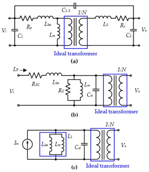
Figure 6.
Simplified analysis of a transformer with: (a) typical model, (b) transferring to the primary side circuit and (c) the Norton equivalent circuit.
The simplified circuit [13] shown in Figure 6b is used for the transformer design. Assuming ideal conditions (i.e., neglecting winding resistance RSC and conversion loss resistance RC), representing by the Norton equivalent circuit shown in Figure 6c, the resonant frequency in the circuit is determined by the equivalent inductance L1 and the total stray capacitance Cstr.
Therefore, as long as the primary-side inductance LP and the natural resonant frequency fr are determined, the simplified transformer model can be derived using the following equations.
where the resonant parameters L1 and Cstr of the transformer are obtained from the simulation results. These two parameters can define the manufacturing specifications of the transformer. In addition, the stray parameters of the transformer depend on the structure, the manufacturing method, and the operating frequency. Especially, most magnetic components still need manual production, and thus the manufacturing error must be considered. Generally, the manufacturer only gives the specification of the parameter LP, the range of the leakage inductance Llea and the turns ratio N.
For example, LP is approximately 5 mH, Llea is about 15% of LP, and N is 20. Here, there is no limit to the stray capacity range, and this may have a significant impact on the performance of the high voltage transformer. To ensure that the actual characteristics agree with the simulated results, the resonant frequency and stray capacitance must be tested after the transformer is manufactured.
Next, various resonant frequencies are calculated to obtain the corresponding stray capacitance Cstr. Table 1 shows the stray parameters under various resonant frequencies. In the simulation circuit, the effects of high-voltage probes and external capacitors are considered. The simulation circuit model of the overall inverter is shown in Figure 7.

Table 1.
Stray parameters with different resonant frequencies.
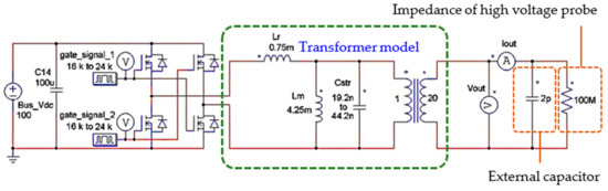
Figure 7.
Simulation circuits of the high-voltage power supply.
Figure 8 shows the simulation results of the gain curves with operating frequencies of 16 to 24 kHz under various resonant frequencies (simulation results for 30, 35, 40, and 45 kHz are shown with solid lines and actual sample test results are shown with the red dashed line). The simulation results imply that if a gentle output gain curve is desired for the operating frequency range, the fabricated transformer must have a resonant frequency of 40 to 45 kHz. This means that the stray capacitance Cstr should be controlled to be approximately 19.6 to 24.9 nF. Thus, the manufacturing parameters of the transformer are defined in Table 1. Finally, the actual parameters of the fabricated transformer are as follows: the resonant frequency = 40.3 kHz, Llea = 0.77 mH, Lm = 4 mH, and Cstr = 24.2 nF.
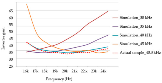
Figure 8.
Characteristic curves with different resonant frequencies.
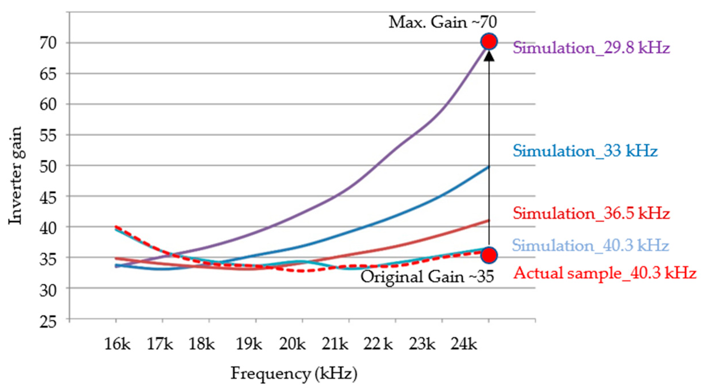
In order to analyze the maximum load capacitance, we refer to the reference [23]. The conversion ratio of the capacitance value between the primary and secondary sides of an ideal transformer is 1: N2 (N is turn ratio). Affected by the turns ratio, it can be seen that as output load capacitance increases, the capacitance value of the primary side conversion also increases so that the resonance frequency of the primary side will be lower. We use the parameters of the actual transformer to draw the gain curve of the lower resonance frequency, as shown in Figure 9, and it can be seen that the lower the resonance frequency, the higher the gain value.
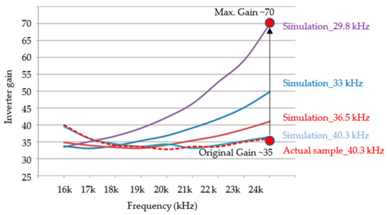
Figure 9.
Selecting the frequency curve of the maximum gain.
In order to avoid the large current of the high gain damaging the transformer, we use the actual transformer parameters in the simulation and change the output capacitance to obtain the gain curves of different resonant frequencies. The frequency curve of the maximum gain is selected, then the maximum load capacitance value can be obtained through reverse calculation. The maximum gain is assumed not to exceed twice the original gain. In Figure 9, the maximum gain is about 70 for 29.8 kHz, almost double the original maximum gain for 40.3 kHz. Therefore, the frequency of 29.8 kHz is the lowest resonance frequency allowed. Table 2 shows the corresponding calculation results. The maximum capacitance of the secondary side is 110 pF, the no-load output capacitance is 60.2 pF, and the high voltage probe and other calibration capacitance is 2 pF. Thus, it is shown that the secondary side capacitance margin is 47.8 pF, and it is recommended to use a plasma generator with a load capacitance less than this value.
Table 2.
Corresponding calculation.
In addition, one can compensate the resonant frequency through a passive filter to solve the matching problem between the power supply and the plasma jet. Due to a high number of turns in the output winding of the high voltage transformer, the inductance value of the output side is considerable. If an inductance device is used in a passive filter to compensate for the resonance frequency on the secondary side, its inductance value must be immense, and the volume of the output stage hence increases. This problem can be solved by increasing the inductance on the primary side, or a pF-scale high-voltage capacitor can be used on the secondary side to do the compensation. This compensation method can make the circuit volume relatively small.
3.2. PFC Converter
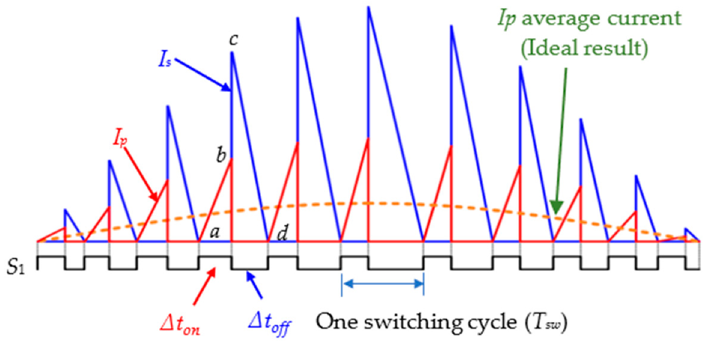
A high-power-factor power supply generally uses a boost topology to transform different AC inputs into a fixed high-voltage DC source. However, this study uses a flyback converter [18] that can perform output regulation and meets the universal AC voltage range. The designed power is approximately 60 W in the continuous output state. Therefore it is recommended that this power supply uses a plasma load of less than 50 W. The circuit used the off-shelf ASICs L6562 and TSM101 to realize this PFC converter, and the designed circuit is shown in Figure 10. The working principle of the circuit is based on the chopper of the power electronics. Once an electrical power switch turns on and off hundreds of times under a sinusoidal voltage with a low frequency of around 50 to 60 Hz, the primary-side current Ip and secondary-side current Is will become triangular waveforms due to the inductance property of a transformer. The input current is controlled by adjusting the duty ratio in each switching cycle.
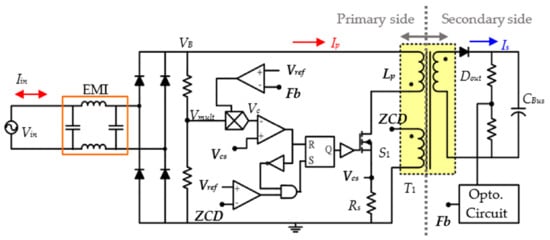
Figure 10.
The PFC circuit control block.
If the duty ratio adjustment is based on the input sinusoidal voltage Vmult, the input current will be transformed to have the same amplitude and waveform as those of the voltage signal during the repeated power on/off switching process, as shown by the red current waveform Ip in Figure 11. An electromagnetic interference (EMI) filter, which filters high-frequency signals, is placed ahead of the PFC converter. The input current Iin is then averaged to a sinusoidal-like wave. Ideally, the input current waveform is corrected to approximate the input voltage waveform, as shown by the fine dotted line in Figure 11.

Figure 11.
The PFC circuit working waveform.
The AC main voltage input is passed through a bridge rectifier to obtain half-wave voltage VB, and a voltage divider circuit is employed to detect the low-voltage half-wave signal Vmult. In addition, the signal Fb passes through an optocoupler circuit from the secondary-side feedback to the primary side, and is then connected to the inverting port of the error amplifier. The control reference Vc can be determined by multiplying the output of the error amplifier by Vmult.
Therefore, when the input and output voltages differ, the voltage level of Vc will change. Vc is compared with the signal Vcs and then assigned to the input R of the RS flip-flop, where Vcs is the obtained voltage signal by the resistor Rs, proportional to the primary inductor current Ip. The signal at the input S is defined as the zero current detection (ZCD), and the output Q is the PWM signal of the control. In a switching cycle, the PFC circuit working process is described as below.
3.2.1. Power Switch S1: Turn On → Turn Off
When the power switch S1 is turned on, the transformer enters a magnetized state, and thus the inductor current Ip rises linearly with proportionally increasing voltage Vcs, as shown from point a to point b on the Ip curve in Figure 11. This state remains until the comparator’s positive input voltage Vcs is greater than the negative input voltage Vc, and then the input R of the RS flip-flop changes to the high level, while both input S and output Q of the RS flip-flop change to a low level. The signal Q is amplified to turn off power switch S1 so that the transformer starts to release energy and charge the output capacitor on the secondary side, as shown from point c to point d on the Ip curve in Figure 11. Simultaneously, the transformer winding polarity changes so that the voltage of ZCD changes from a low level to a high level, and the current Ip drops to zero and thus the input R of the RS flip-flop is restored to a low level. Therefore, both the input S and the input R of the RS flip-flop are still at a low level, and S1 remains off until the current Is decreases to zero.
3.2.2. Power Switch S1: Turn Off → Turn On
When the current Is reduces to zero, the transformer winding polarity is restored so that the voltage of ZCD changes from a high level to a low level. The comparator’s negative input ZCD is lower than the positive input voltage Vref, so the comparator’s output changes to a high level and the input S of the RS flip-flop changes to a high level as well. The input R of the RS flip-flop is still at a low level. Therefore, the output Q of the RS flip-flop changes to a high level. Eventually, the signal Q is amplified again to turn on the power switch S1 and the transformer begins to store energy while the current Ip rises linearly until Vcs > Vc again.
The power switching action has been defined for a switching cycle. The circuit system is controlled by the input or output status. When the output voltage drops, the feedback voltage signal Fb also decreases, and therefore the error signal increases, making the control signal Vc larger. As a result, the peak current of the primary side becomes higher, indicating an increase of the average input current, and hence provides more energy to regulate the level of the output voltage. When the output voltage exceeds its operating level, the voltage of the feedback signal Fb rises, so the reference signal Vc decreases. Therefore, it can be ensured that this PFC flyback converter maintains a constant output voltage. Because this PFC is a frequency-varying and duty-ratio-varying control device and the inductance value determines the operating frequency of the PFC circuit [21], the inductance value Lp of the primary side in the transformer dominates the design of the PFC circuit. The derivations of the inductance value of the transformer and working frequency are given below. The input voltage and current are defined as ideal sinusoidal waves as:
where Vin_pk and Iin_pk are the peak values of the input voltage and current, respectively. The term f is the frequency of the input, which is either 50 or 60 Hz. Assuming that the transformer of the PFC circuit is ideal, the current of the secondary side is defined as follows:
because this PFC converter operates in discontinuous current boundary mode [18], a single switching period Tsw equals the sum of the turn-on time and the turn off time , is shown by the current control condition in Figure 11.
The voltage of the inductor is: . When the power switch is turned on, L becomes Lp, the primary inductance of the transformer. The voltage VL of the primary-side coil equals the input voltage Vin_pk. is the current change from zero to Ip_pk, as shown by the a-b segment in Figure 11. Then, is given as:
and when the power switch is turned off, . The voltage VL of the primary-side coil equals the output voltage Vout plus the forward voltage Vout_diode of the output diode, multiplied by the coil ratio n. Let be the current change from zero to Ip_pk, as shown by the c-d segment in Figure 11. Then, is given as:
Combining Equations (9) and (10) yields:
Let the primary-to-secondary reflected voltage VR equal n·(Vout + Vout_diode) and the switching frequency equal , then, the inductance of the primary side is given as:
where Vin_pk is the maximum voltage and Ip_pk is the current in a sinusoidal waveform. Finally, the inductance value of PFC at the working frequency can be derived from Equation (11).
4. Test Results
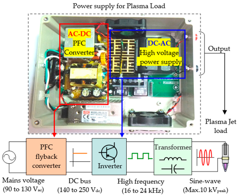
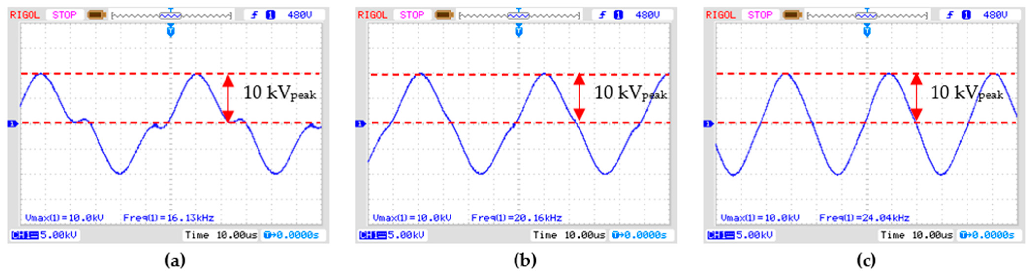
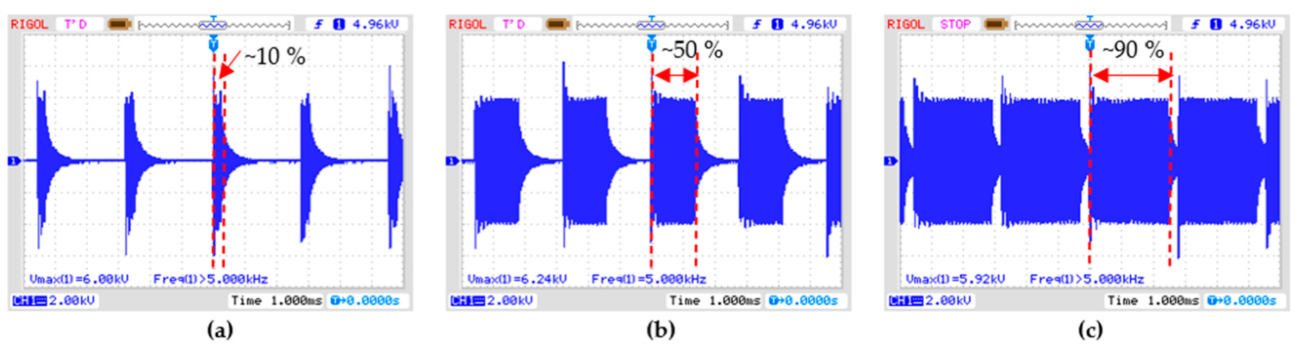
The internal configuration of the implemented high-voltage power supply of this paper is shown in Figure 12. There are two independent power stages in the box. In the first power stage, the DC bus voltage is roughly regulated in the range of 140 to 250 Vdc from the main input voltage of 90 to 130 Vac by the PFC converter. In the second power stage, the inverter is combined with a full-bridge circuit and a high-voltage transformer to perform a boost function, resulting in the generation of a high-voltage sinusoidal wave. The test results without load are shown in Figure 13. It shows that the peak voltage value can reach 10 kVpeak at different frequencies. Moreover, the output voltage uses the waveform controlled by the burst mode, as shown in Figure 14, and it can have 10~90% control options.

Figure 12.
Power supply photo and schematic diagram.
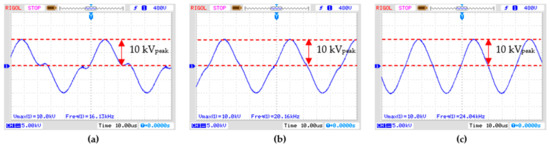
Figure 13.
Output voltages at different frequencies: (a) 16 kHz (b) 20 kHz and (c) 24 kHz.
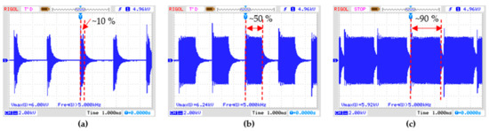
Figure 14.
Burst output mode: (a) 10% (b) 50% and (c) 90%.
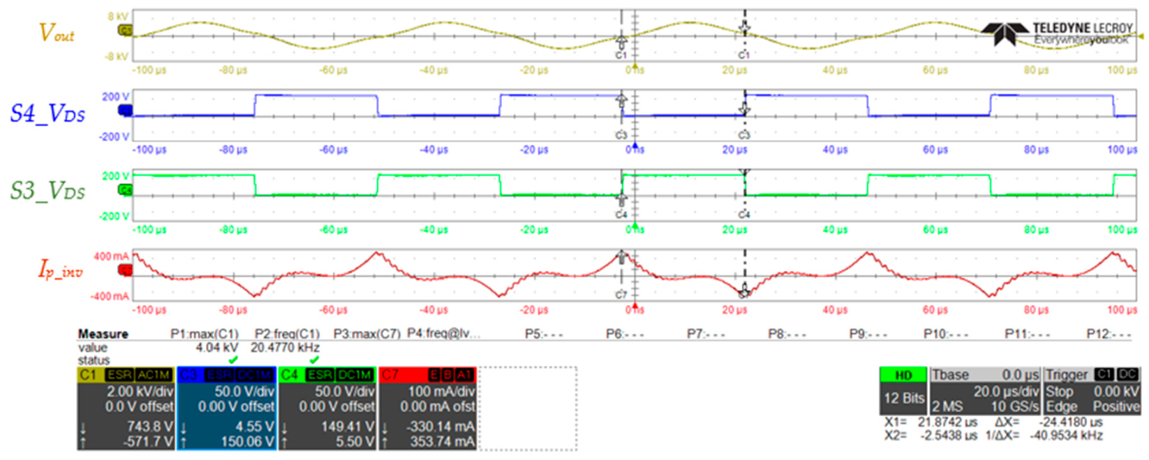
Figure 15 shows the working waveforms of the full-bridge circuit, and we measured the drain to source voltages of low-side switches (S3_VDS, S4_VDS), primary side current (Ip_inv) and output voltage (Vo_peak). It can be seen from the waveforms that the loop current is not zero when the switches are switching, so this circuit has no soft-switching ability. This working current is small, and the power consumption is also low despite switching loss. The primary side only needs a 0.4 A peak current for the output voltage on the secondary side to reach 4 KVpeak without load.

Figure 15.
Full-bridge circuit working waveform.
We conducted an efficiency test with about 10 watts output to validate the efficiency value of each module in the overall circuit. In order to render the test data repeatable, in the experiment, a high-voltage resistance (10 kV 1 Mohm) was used as the test load, and the test results are given in Table 3. A comparison of the characteristics of the proposed power supply and the commercially available one in the case study is summarized in Table 4. It is shown that the proposed power supply is both smaller and lighter, and optimizes the electrical characteristics of the input end. Although the output voltage of the proposed design is smaller than that of PVM500, the proposed design outperforms PVM500 in all other items. It demonstrates the practicality of the proposed design.
Table 3.
Circuit efficiency measurement.
Table 4.
Comparison of different HV power supplies.
To further assess the performance, we performed a load test of the power supply with the APPL jet. Figure 16a shows the Helium APPJ and high-voltage Power Supply test setup before packaging. Figure 16b shows the packaged prototype. The power supply panel includes voltage and frequency control knobs, LED ON/OFF indicators, and a power ON/OFF switch. The high-voltage wire and gas supply tube were inserted from the top of the APPJ, and the quartz tube and electrodes were sealed using insulator glue in a plastic shell.
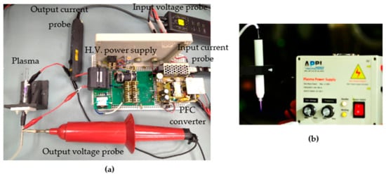
Figure 16.
Test setup photos: (a) setup before packaging and (b) packaged prototype.
4.1. Measurement and Simulation Verification
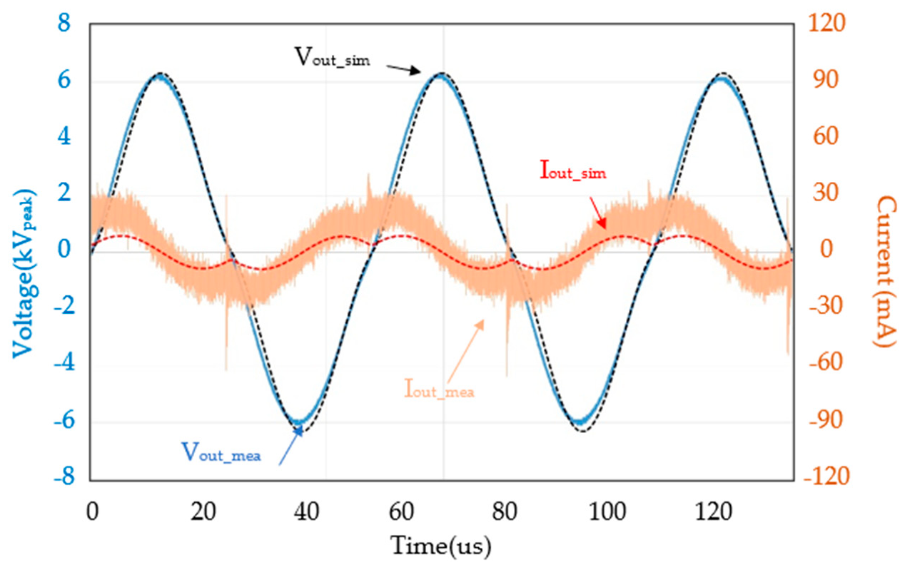
In the tests, the helium flow rate was 5 slm in the APPJ. The operating peak voltage of the power supply was in the range of 4 to 6 kVpeak, and the frequency was about 20.9 kHz. The output waveforms were measured using an oscilloscope (LeCroy WS44XS-A) via a high-voltage probe (Tektronix P5100) and a current probe (Pearson 3972). Figure 17 shows the measured voltage and current waveform. By observing the waveform, it is seen that the current phase of the APPJ is about 90° ahead of the voltage phase, when driven by a sinusoidal AC signal. Such a waveform is similar to the result given in [7], which means the APPJ is a capacitive load.
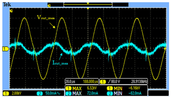
Figure 17.
Actual measurement results.
In addition, a high-frequency surge occurred in the current waveform. The cause is that the switching frequency is different from the natural frequency of the transformer. When the inverter is switching, the output current is forced to change direction. The parasitic inductor and capacitor in the circuit loop produce the high-frequency resonance in the transient changes; thus, there are high surges in the current.
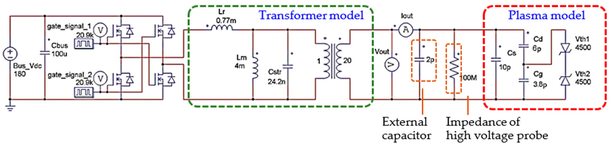
For verification, the simulation was conducted with the operating conditions the same as the experiment (output frequency 20.9 kHz, input voltage of inverter 180 Vdc). The model for the simulation circuit is shown in Figure 18; the full-bridge inverter, transformer model, high-voltage probe impedance and plasma jet model are included. First, to obtain the parameters of the plasma model, we measured the dimensions of the actual plasma jet. We obtained a = 1.5 mm, b = 2 mm, c = 4 mm, and l = 20 mm, as shown in Figure 1. The relative dielectric constants of quartz and air are = 3.8 and = 1, respectively. Substituting these constants into Equations (3) and (4) yields Cd = 6 pF and Cg = 3.8 pF, and the power consumption resistor R is set to around 10 kΩ. In addition, the stray capacitor Cs is about 10 pF, obtained by measuring the output connection wire.
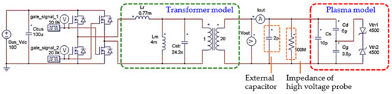
Figure 18.
Simulation circuits of power supply, transform model, and plasma model.
The helium APPJ used in this work has a breakdown voltage of about 4 to 5 kVpeak at the normal pressure, according to previous experimental results [3]. Therefore, we set the breakdown voltage to 4.5 kVpeak. Second, the manufacturer’s transformer parameters are as follows: (1) the transformer turns ratio is 1:20; (2) the equivalent parameters of the transformer are a magnetizing inductance of LP = 4.77 mH and leakage inductance of Lr = 770 µH; and (3) the resonant frequency is about 40.3 kHz.
Figure 19 shows the results of the experiment and simulation. The solid lines are the measured voltage and current (Vout_mea, Iout_mea), and the dashed lines are the simulated voltage and current (Vout_sim, Iout_sim). It can be seen that the voltage in the simulation has good agreement with the experimental measurement, and there is a difference in the amplitude of output current between the simulation and experimental result. We think this deviation may be because the discharge consumption is not defined in the plasma model, and the actual impedance of the gas in the discharge state is unknown. Although this paper uses a general and less precise plasma model in the simulation-based design, it can allow the designer to quickly determine the gas discharge load’s approximate working range and waveform. In further analysis, we suggest adding the load impedance and adjusting the connecting wire’s stray capacitance Cs to correct the simulation results.
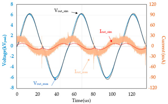
Figure 19.
Actual measurement and simulation.
4.2. PFC and Output Ripple
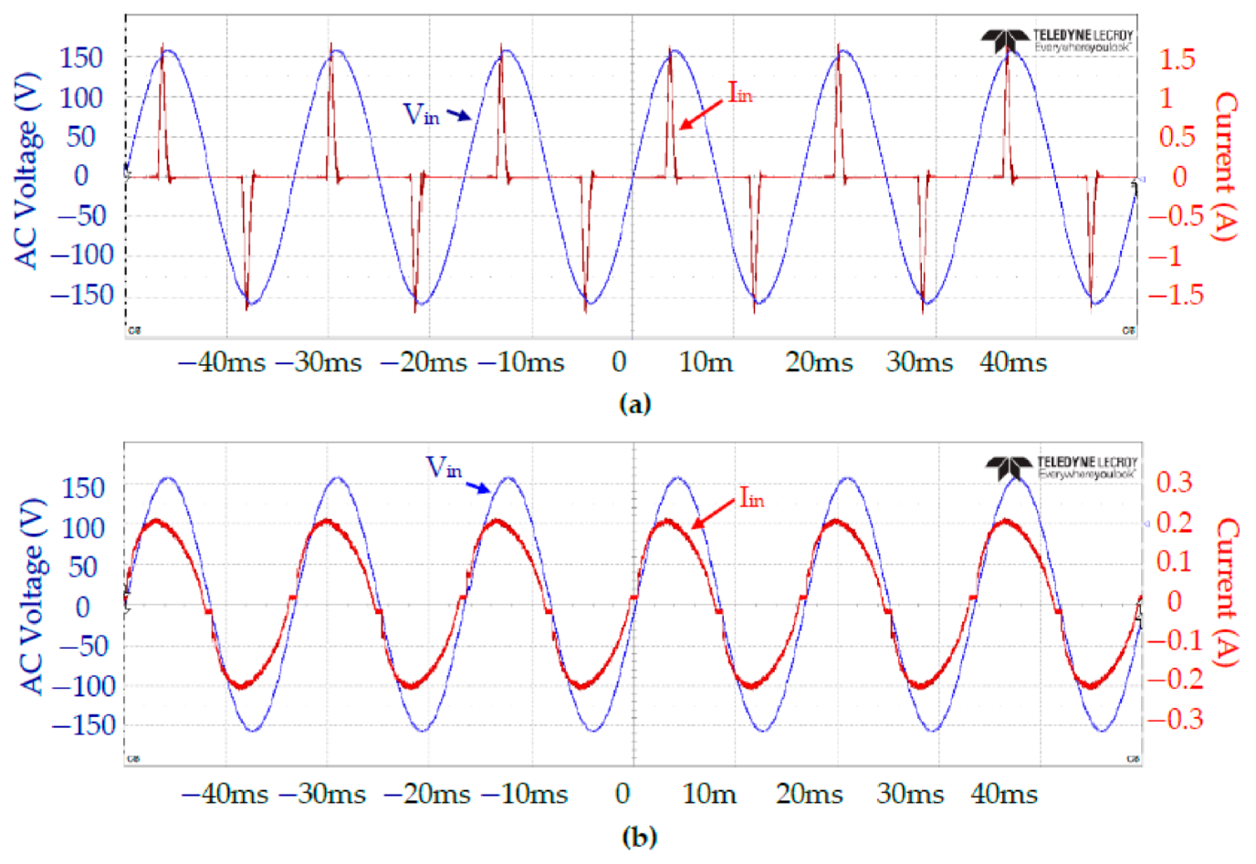
Following the PFC circuit design given in Section III, the specifications of the PFC converter are: (1) an input voltage of 90 to 264 Vac and an output voltage of 140 to 250 Vdc; (2) a maximum power of 60 W; (3) a minimum operating frequency of the PFC circuit of 25 kHz; and (4) a transformer core type of PQ3230 with the specifications of le = 67.8 mm, Ae = 153.8 mm2, Ve = 10,440 mm3, core material: SAMWHA PL-9, maximum magnetic flux setting: 2900 G, leakage inductance: about 80 µH, a primary turns to the secondary turns ratio of 66:60 with an inductance value of 730 µH, and air gap = unclear. We tested the input-end performance of the designed plasma power supply under a 110 Vac input voltage. Figure 20a shows that the input current waveform deforms dramatically without PFC, resulting in a power factor of just 0.41. We then replaced the autotransformer with the PFC converter. Figure 20b shows that the input current becomes a nearly sinusoidal wave that is in phase with the input voltage and the resulting power factor is 0.95. Figure 21 also shows that the difference in the harmonic distortion of the current before and after improvement. With PFC, the 1st harmonic component is significantly increased, and the others are reduced. These results verify that satisfactory power quality can be achieved using the proposed plasma power supply.
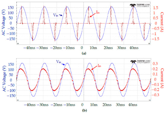
Figure 20.
AC input waveforms obtained: (a) without PFC and (b) with PFC.
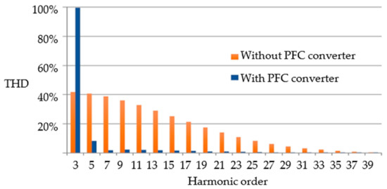
Figure 21.
Total harmonic distortion in the AC input current.
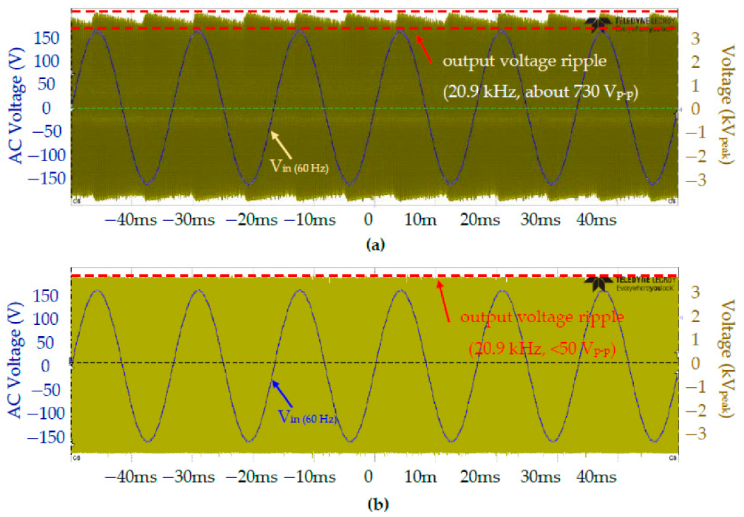
Furthermore, the advantage of using a PFC converter is that it further reduces the output voltage ripple. The range of voltage ripple is reduced from 750 Vp-p to below 50 Vp-p, as shown in Figure 22a,b. Figure 22a shows that the high-voltage power supply uses a rectifier. The output voltage ripple constantly fluctuates with the AC frequency (50~60 Hz). When the output power increases or the internal capacitors age, the issue of the output ripple becomes more serious. However, Figure 22b shows that the high-voltage power supply uses an active PFC converter. Since the converter can generate a smooth DC voltage on the input of the inverter, it thus significantly reduces the voltage variations on the output ripple.
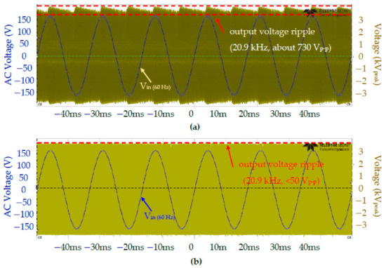
Figure 22.
Improved ripple of the output voltage: (a) without PFC and (b) with PFC.
4.3. OES Test
Plasma jet emission was analyzed using OES. The plastic shell, which contains the APPJ device, was fixed by an insulating holder for further measurement. We set the optical lens to be 15 mm away from the front of the APPJ and analyzed the APPJ emission by OES. The OES system was assembled by a monochromator (Princeton Instruments Acton sp2500) with a photomultiplier tube (Hamamatsu R928).
Figure 23 shows the OES results in the discharge region.The results are a typical spectrum of a helium APPJ, in which hydroxyl radical (309 nm), atomic oxygen (777 nm), helium (706 nm), nitrogen second positive system, and nitrogen first negative system are found in the plasma jet. The working gas was high-purity helium (99.995%), and thus the oxygen and nitrogen species may have come from small impurities in the gas cylinder or ambient air. These reactive oxygen/nitrogen species (RONS) play a crucial role in many applications. For example, oxygen species are essential for surface modification and sterilization [20,21], and nitrogen species are essential for wound healing [22].
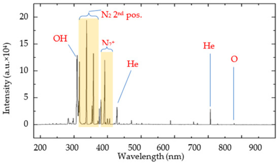
Figure 23.
OES analysis in the discharge region.
The results demonstrate that the developed plasma power supply can sustain the helium APPJ with a high power factor and high RONS intensity, which are essential factors for commercializing an APPJ system.
5. Conclusions
This study successfully miniaturized the plasma power supply by the proposed redesigned high-voltage transformer and combination of a PFC converter and an inverter. The designed power supply is smaller than the conventional design, improves the input power factor, and reduces the output voltage ripples. In the experiments, they have been verified and quantitatively compared. Such features of the proposed design bring advantages to the high-voltage power drivers but can also facilitate the commercial development of the applications of plasma systems. Future design of this power supply, may consider using the soft-switching technique in the inverter. The LLC resonant circuit design concept can be used to improve switching loss on power switches in the inverter, and unlike the DC/DC LLC resonant circuit, the DC/AC high voltage resonant power supply must pay special attention to the load capacitance on the secondary side. It may be necessary to limit the range of load conditions (load and capacitance value) to maintain the advantage of soft switching on the primary side.
Author Contributions
Conceptualization, J.-S.W. and M.-T.H.; Methodology, C.-F.S. and M.-T.H.; Validation, C.-F.S. and C.-T.L.; Formal analysis, C.-F.S. and C.-T.L.; Data curation, C.-F.S.; Writing—original draft, C.-F.S.; Writing—review & editing, J.-S.W. and M.-T.H.; Supervision, J.-S.W. and M.-T.H. All authors have read and agreed to the published version of the manuscript.
Funding
This research received no external funding.
Data Availability Statement
Data collected through research presented in the paper are available on request from the corresponding author.
Conflicts of Interest
The authors declare no conflict of interest.
References
- Kang, H.R.; Chung, T.H.; Joh, H.M.; Kim, S.J. Effects of Dielectric Tube Shape and Pin-Electrode Diameter on the Plasma Plume in Atmospheric Pressure Helium Plasma Jet. IEEE Trans. Plasma Sci. 2017, 45, 691–697. [Google Scholar] [CrossRef]
- Das, S.C.; Majumdar, A.; Mukherjee, S.; Katiyal, S.; Shripathi, T. Development of power supply for atmospheric pressure plasma jet at room temperature for bio-medical applications. In Proceedings of the 3rd International Conference on Computing for Sustainable Global Development (INDIACom), New Delhi, India, 16–18 March 2016; pp. 1207–1209. [Google Scholar]
- Liu, C.-T.; Wu, C.-J.; Lin, Z.-H.; Wu, J.-Y.; Wu, J.-S. Production Enhancement of Reactive Oxygen and Nitrogen Species at Interface of Helium Plasma Jet and Agar. IEEE Trans. Plasma Sci. 2016, 44, 3112–3116. [Google Scholar] [CrossRef]
- Kim, G.C.; Han, M.S.; Nam, S.H. Evaluation of tooth staining with red wine after tooth bleaching with nonthermal atmospheric pressure plasma. Biomed. Res. 2018, 29, 396–400. [Google Scholar]
- Bernhardt, T.; Semmler, M.L.; Schäfer, M.; Bekeschus, S.; Emmert, S.; Boeckmann, L. Plasma Medicine: Applications of Cold Atmospheric Pressure Plasma in Dermatology. Oxidative Med. Cell. Longev. 2019, 4, 1–10. [Google Scholar] [CrossRef] [PubMed] [Green Version]
- 1–40 kV 20–70 kHz 10–300 W Adjustable Power Supply. 1–40 kV 20–70 kHz 10–300 W Adjustable Power Supply (<50 pfd loads)—Information Unlimited. Available online: amazing1.com (accessed on 4 August 2021).
- Fuentes, A.F.; Eguiluz, R.P.; Callejas, R.L.; Cabrera, A.M.; Alvarado, R.V.; Delgado, S.B.; de la Piedad-Beneitez, A. Electrical Model of an Atmospheric Pressure Dielectric Barrier Discharge Cell. IEEE Trans. Plasma Sci. 2009, 37, 128–134. [Google Scholar] [CrossRef]
- Judée, F.; Vaquero, J.; Guégan, S.; Fouassier, L.; Dufour, T. Atmospheric pressure plasma jets applied to cancerology: Correlating electrical configurations with in vivo toxicity and therapeutic efficiency. J. Phys. D Appl. Phys. 2019, 52, 1–16. [Google Scholar] [CrossRef] [Green Version]
- Wang, R.; Yang, Y.; Chen, S.; Jiang, H.; Martin, P. Martin. Power Calculation of Pulse Power-Driven DBD Plasma. IEEE Trans. Plasma Sci. 2021, 49, 2210–2216. [Google Scholar] [CrossRef]
- Florez, D.; Diez, R.; Piquet, H. DCM-Operated Series-Resonant Inverter for the Supply of DBD Excimer Lamps. IEEE Trans. Ind. Appl. 2014, 50, 86–93. [Google Scholar] [CrossRef] [Green Version]
- Joh, H.M.; Kang, H.R.; Chung, T.H.; Kim, S.J. Electrical and Optical Characterization of Atmospheric-Pressure Helium Plasma Jets Generated With a Pin Electrode: Effects of the Electrode Material, Ground Ring Electrode, and Nozzle Shape. IEEE Trans. Plasma Sci. 2014, 42, 3656–3667. [Google Scholar] [CrossRef]
- Bonnin, X.; Brandelero, J.; Videau, N.; Piquet, H.; Meynard, T. A High Voltage High Frequency Resonant Inverter for Supplying DBD Devices with Short Discharge Current Pulses. IEEE Trans. Plasma Sci. 2014, 29, 4261–4269. [Google Scholar] [CrossRef] [Green Version]
- Nong, C.Y.; Ming, K.C. Design of Plasma Generator Driven by High-frequency High-voltage Power Supply. J. Appl. Res. Technol. 2013, 11, 225–234. [Google Scholar] [CrossRef]
- Diaz, F.J.; Azcondo, F.J.; Casanueva, R.; Brañas, C. Power Source Electronic Ballast for Electrodeless Fluorescent Lamps. Electronics 2020, 9, 34. [Google Scholar] [CrossRef] [Green Version]
- Cheng, C.A.; Cheng, H.L.; Ku, C.W.; Chung, T.Y. Design and Implementation of a Single-Stage Acoustic-Resonance-Free HID Lamp Ballast with PFC. IEEE Trans. Power Electron. 2014, 29, 1966–1976. [Google Scholar] [CrossRef]
- Rabkowski, J.; Lasica, A.; Zdanowski, M.; Wrona, G.; Starzynski, J. Portable DC Supply Based on SiC Power Devices for High-Voltage Marx Generator. Electronics 2021, 10, 313. [Google Scholar] [CrossRef]
- Taherian, M.; Allahbakhshi, M.; Farjah, E.; Givi, H. An Efficient Structure of Marx Generator Using Buck–Boost Converter. IEEE Trans. Plasma Sci. 2018, 46, 117–126. [Google Scholar] [CrossRef]
- Nara, K.; Channegowda, J. Single Stage PFC Flyback AC-DC Converter Design. In Proceedings of the IEEE International Conference on Electronics, Computing and Communication Technologies (CONECCT), Bangalore, India, 2–4 July 2020; Volume 46, pp. 1–6. [Google Scholar]
- Das, S.; Sudhakar, P. Power Factor Correction & Harmonic Distortion Control for AC-DC Fault Tolerant Power Distribution System & Power Quality Qualification Test Results as per IEC 61000-3-2. BARC Newsl. 2017, 356, 5–13. [Google Scholar]
- Liu, C.T.; Kumakura, T.; Ishikawa, K.; Hashizume, H.; Takeda, K.; Ito, M.; Hori, M.; Wu, J.S. Effects of Assisted Magnetic Field to An Atmospheric-Pressure Plasma Jet on Radical Generation at The Plasma-Surface Interface and Bactericidal Function. Plasma Sources Sci. Technol. 2016, 25, 065005. [Google Scholar] [CrossRef]
- Kostov, K.G.; Nishime, T.M.C.; Castro, A.H.R.; Toth, A.; Hein, L.R.O. Surface Modification of Polymeric Materials by Cold Atmospheric Plasma Jet. Appl. Surf. Sci. 2014, 314, 367–375. [Google Scholar] [CrossRef] [Green Version]
- Witte, M.B.; Kiyama, T.; Barbul, A. Nitric Oxide Enhances Experimental Wound Healing in Diabetes. Br. J. Surg. 2002, 89, 1594–1601. [Google Scholar] [CrossRef] [Green Version]
- Kwon, J.; Kim, R.-Y. High Power Density, High-Voltage Parallel Resonant Converter Using Parasitic Capacitance on the Secondary Side of a Transformer. Electronics 2021, 10, 1736. [Google Scholar] [CrossRef]


Publisher’s Note: MDPI stays neutral with regard to jurisdictional claims in published maps and institutional affiliations. |
© 2021 by the authors. Licensee MDPI, Basel, Switzerland. This article is an open access article distributed under the terms and conditions of the Creative Commons Attribution (CC BY) license (https://creativecommons.org/licenses/by/4.0/).