Article

Development of a Real-Time Magnetic Field Measurement System for Synchrotron Control

1
CERN, European Organization for Nuclear Research, 1 Esplanade des Particules, 1217 Meyrin, Switzerland
2
Faculty of ICT, University of Malta, MSD 2080 Msida, Malta
3
Department of Electronics and Telecommunications (DET), Polytechnic University of Turin, 10129 Turin, Italy
4
Department of Electrical Engineering and Information Technology (DIETI), University of Naples Federico II, 80100 Naples, Italy
*
Author to whom correspondence should be addressed.
Electronics 2021, 10(17), 2140; https://doi.org/10.3390/electronics10172140
Submission received: 17 July 2021 / Revised: 19 August 2021 / Accepted: 20 August 2021 / Published: 2 September 2021
(This article belongs to the Section Systems & Control Engineering)

Abstract

:
The precise knowledge of the magnetic field produced by dipole magnets is critical to the operation of a synchrotron. Real-time measurement systems may be required, especially in the case of iron-dominated electromagnets with strong non-linear effects, to acquire the magnetic field and feed it back to various users. This work concerns the design and implementation of a new measurement system of this kind currently being deployed throughout the European Organization for Nuclear Research (CERN) accelerator complex. We first discuss the measurement principle, the general system architecture and the technology employed, focusing in particular on the most critical and specialized components developed, that is, the field marker trigger generator and the magnetic flux integrator. We then present the results of a detailed metrological characterization of the integrator, including the aspects of drift estimation and correction, as well as the absolute gain calibration and frequency response. We finally discuss the latency of the whole acquisition chain and present an outline of future work to improve the capabilities of the system.

1. Introduction

In synchrotrons, precise knowledge of the average bending field in the dipole magnets is essential for transversal and longitudinal beam control [1]. At CERN, six machines, namely the Low Energy Ion Ring (LEIR), Proton Synchrotron (PS), PS-Booster (PSB), Super Proton Synchrotron (SPS), Antiproton Decelerator (AD) and Extra Low ENergy Antiproton deceleration ring (ELENA), employ a so-called B-train for determining the dipole field. The name derives from the discrete positive and negative pulse trains used to incrementally distribute the measured field in legacy systems, developed as far back as the 1950s [2]. The B-train measures the average field of a reference magnet and distributes the result in real-time to various other synchrotron sub-systems as part of a feedback control loop or for diagnostic purposes. As an example, the ELENA ring and its B-train reference magnet are shown in Figure 1. The typical range of the magnetic field measured goes from about 50 m T to 2 T . The need for a real-time measurement system stems from the difficulty to predict an accurate value of the average field, a consequence of non-linear effects such as eddy currents, saturation and hysteresis inherent to iron-dominated magnets, which are dependent upon the magnetic properties of the iron core and the history of the excitation current. The most critical user of the B-train is the Radio Frequency (RF) subsystem, which uses RF cavities to generate the electric field that accelerates or decelerates the beam. The instantaneous magnetic field must be known with high precision to lock the RF frequency to the particle energy, keeping the beam centred in the vacuum chamber. While the pass-band of the bending magnets does not usually exceed a few hundred hertz, the RF system requires a much faster data rate to ensure smooth feedback, e.g., 250 k Hz in the PS. The use of B-train systems is not unique to CERN: for instance, similar designs are implemented at ion therapy centres such as the National Centre of Oncological Hadrontherapy (CNAO) [3], MedAustron [4] and the Heidelberg Ion-Beam Therapy Centre (HIT) [5]. For such applications, real-time feedback control of the magnetic field is instrumental, for example, to reduce dead times that would be otherwise spent pre-cycling the magnets to improve their reproducibility. This paper presents a novel B-train system called FIRESTORM (Field In REal-time STreaming from Online Reference Magnets), developed to replace the existing systems in the context of a site-wide, long-term consolidation project. FIRESTORM has been designed to cope with the High-Luminosity Large Hadron Collider upgrade, which will require higher beam intensity and improved beam control throughout the injector chain [6]. After an extensive, successful test phase [7], deployment is currently ongoing across the CERN complex with the new systems expected to be fully operational for the upcoming LHC physics run. In Section 2 and Section 3 of this work, we discuss the broad measurement principle and overall architecture of the system. Section 4 describes the custom electronic components implemented. In Section 5, we present the results of a test campaign focused on the performance of the integrator, with measurements of the overall latency of the system given in Section 6. Finally, in Section 7, we provide our concluding remarks and outline future work.

2. Measurement Goals and Method

The main goal of a B-train system is to measure and distribute the average dipole magnetic field, B ¯ , that bends the trajectory of the beam in a synchrotron ring. The magnetic field varies cyclically over time, as illustrated in Figure 2, being proportional to the momentum of the beam particles as they are first injected into the ring, then accelerated and finally ejected. Typical requirements include a measurement uncertainty of 100 ppm relative to the peak field during a cycle, a bandwidth from DC to 100 Hz , and a maximum latency of 30   μ s , which is critical especially for the RF subsystem. The measurement is carried out in a suitable reference magnet, which is ideally installed in a dedicated room outside of the synchrotron and is powered in series with the ring magnets. In this case, the absence of a vacuum chamber in the magnet gap leaves the freedom to install sensors along the magnet’s longitudinal axis, where the beam is supposed to circulate. When this is not practical, such as in the LEIR bending dipole, sensors must be installed within the accessible fringe field region. Along with B ¯ , the system also distributes the rate of change of the magnetic field, B ¯ ˙ . This is needed by some machines, such as the PS, which implement multiple excitation circuits that act in parallel on the same magnetic core in order to compensate for induced voltages stemming from inductive coupling effects [8].

2.1. Measurement Model

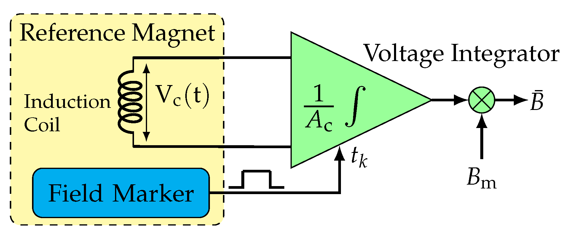
The setup for all B-train systems at CERN consists of the combination of two primary sensors [9,10], as shown schematically in Figure 3: an induction coil to measure the rate of change of the field according to Faraday’s law, and a so-called field marker to provide the necessary integration constant B m , according to Equations (1)–(3):
Φ = A N T B d A = B ¯ A c ,
V c = d Φ d t ,
B ¯ ( t ) = B m + Δ B ¯ ( t ) = B m 1 A c t k * t V c ( τ ) d τ ,
where Φ is the total magnetic flux linked though the coil, N T is the number of coil winding turns, A c is the effective coil area, and V c is the coil output voltage.
The B-train system must operate uninterrupted over periods that may last for months. The integration process is seamlessly subdivided into a sequence of contiguous integration intervals matching the magnetic cycles t k * t < t k + 1 * , with k = 1 , 2 , , where each t k * corresponds to a field marker trigger generated when the field crosses the given threshold B m , practically resetting the process with a new integration constant. By far, the most important error source in Equation (3) is the drift of the integral due to a small, but unavoidable, voltage offset added to the coil output. The problem of voltage offsets in integrators is well-known not only for induction coils but also in different measurement domains, such as inertial sensor [3,11,12]. The offset, which typically ranges in value from a few to a few hundred μ V , is generated by a number of different mechanisms such as thermoelectric voltages due to temperature gradients along wires; thermocouple voltages at the connections; rectification by non-linear circuit elements of radiated EM noise; or bias currents due to the imbalance in discrete or IC components. While some degree of mitigation can be afforded by the thermalization of the whole setup and by careful EMI shielding, the offset can never be eliminated completely [11].
Even if, in principle, the integration constant could be set just once at the beginning of the process, the use of repeated resets effectively prevents the build-up of integrator drift; methods to control the drift within each integration interval are discussed in Section 4.3. The value of B m is often chosen so that a reset happens just before the injection of particles into the synchrotron, when high measurement accuracy is required to capture the incoming beam and preserve its quality. If a reset does occur when the beam is already circulating, B m must not be assigned to B ¯ ( t k ) abruptly but rather in a gradual manner over a suitable interval, of the order of 10 m s , to prevent any discontinuity that may be harmful. During a magnetic cycle, any given field value B m will be crossed twice: once on the up-ramp and once on the down-ramp, thus generating two separate field marker triggers. However, in the current implementation of FIRESTORM, the field marker signal is gated by a specific time window to avoid spurious noise-induced triggers, thereby generating only one reset trigger per cycle. It is worth noting that two fully independent markers can be assigned to any integration channel, allowing for the reset timing to be optimised, as dictated by the beam quality requirements. A typical application of this feature consists of adding a second marker at high field, just at the beginning of the beam ejection plateau, as depicted in Figure 2.

2.2. Induction Coil

The induction coil provides the dynamic component of the field with intrinsically high linearity and bandwidth. Induction coils for accelerator magnets typically consist of multiple loops of single- or multi-filament strands wound around a long, rectangular core [10], where the polarity of the coil’s output is chosen in such a way as to be consistent with the sign of the magnetic field, as given by (3). Since the main quantity of interest for beam control is the longitudinal integral of the magnetic field, the length of the coil is ideally that of the iron yoke, plus the whole fringe field region (typically, 3 to 4 times the gap height at each end) [13]. In some of the systems at CERN, where this is not possible due to space constraints, a much shorter coil is used instead; this is the case in the PS and LEIR, where the coils used are, respectively, about 0.3   m and 0.1   m long, compared with iron yoke lengths of approximately 5 m . In such a case, the average field is assumed to be proportional to the local field seen by the coil. Methods to assess and reduce the error of this approximation due to non-linear effects, such as saturation, hysteresis and eddy currents, are currently under study [14]. The effective area of the coil can be calibrated within a typical uncertainty of 100 ppm by means of the classical flip-coil method, i.e., by immersing it in a sufficiently uniform magnetic field B perpendicular to its surface, turning it over by 180 and measuring the flux change Δ Φ , corresponding to twice the magnetic flux through the coil Φ = A c B . Alternatively, the flux measured by pulsing the field when the coil is kept fixed can be compared to another reference method, such as a single stretched wire [10]. It is important to stress that, for synchrotron control applications, the absolute calibration of the measurement is of secondary importance with respect to its reproducibility. In fact, during the accelerator setup phase, the relationship between the bending field and RF frequency is always adjusted to compensate for many sources of systematic errors, including possible errors in the magnetic field measurement itself, provided these remain reasonably small [15]. Once the operational settings have been fixed, however, they are expected not to change over periods of time of the order of one year, which is normally the interval between major maintenance stops.

2.3. Field Marker

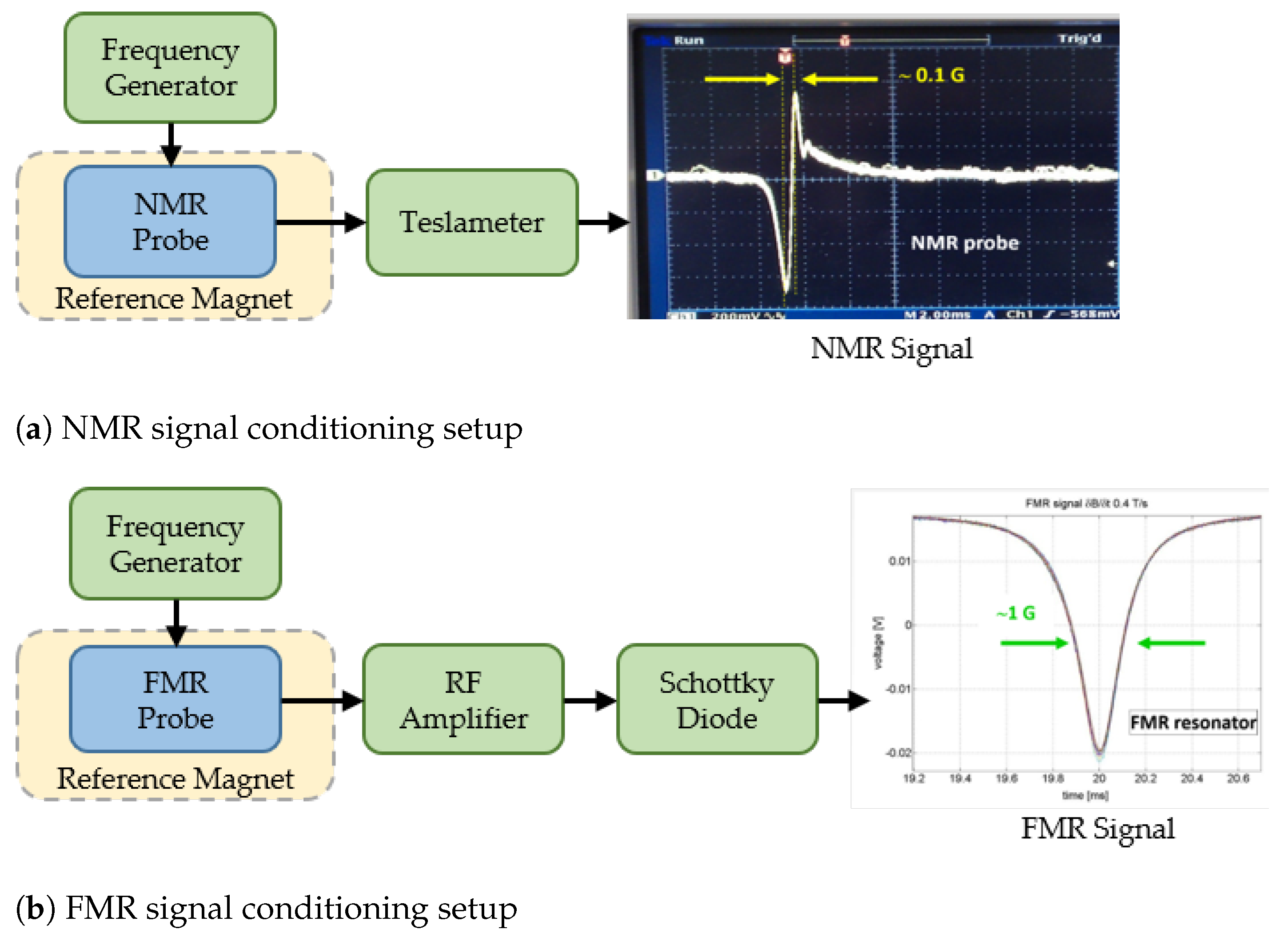
The field marker serves two critical roles in the system: providing the integration constant in (3) and periodically resetting the measurement to prevent the accumulation of drift. The marker itself is composed of a magnetic sensor, together with detection electronics (described in Section 4.2). It generates a digital trigger pulse whenever the field crosses a pre-set value B m . As such, this device has an inherently dynamic nature; detection can only occur on a field ramp. A variety of different sensors can be used for this purpose. The simplest option is a Hall probe combined with a voltage comparator. Even though this method is used with success at CNAO [16] and HIT [12], the long-term stability of the offset and gain of Hall probes may be problematic and entail frequent interruptions for recalibration, which are not acceptable for the CERN accelerator chain. The old PS B-train worked satisfactorily over as many as five decades with a so-called peaking strip, described in [17]. However, this marker operates at a very low field of 5   m T and cannot be scaled easily to higher levels. Instead, the FIRESTORM B-train implements magnetic resonance sensors, which have been extensively tested and proven to meet all requirements [18,19,20]. These sensors are based on the precession frequency of the elementary magnetic moments (protons or electrons) in a small sample of suitable material. The sample is immersed in a background field B and irradiated with electromagnetic waves at a frequency f so that at resonance, it absorbs and re-emits at the frequency f = γ B , where γ is the gyromagnetic ratio. In continuous–wave (CW) mode, the RF excitation frequency is kept fixed, and a sharp peak is produced in the output voltage as the background field sweeps through the resonance. Two different types of CW setups have been developed (see Figure 4):
  • The earliest solution is based on a commercially available instrument: the Nuclear Magnetic Resonance (NMR) teslameter Metrolab PT2025 [17,21,22]. The probe contains a cylindrical sample with a volume of 226 m m 3 made of a hydrogen-rich substance, water or rubber, where resonance is induced in the hydrogen nuclei based on the gyromagnetic ratio of the proton, γ p = 42.57747892(29) MHz/T. This instrument represents a reference standard in magnetometry, as it provides the modulus of the magnetic field with an absolute accuracy of about 5 ppm provided that the field is sufficiently uniform (tolerated relative gradient 1 % / m ) and stable. NMR probes have been used with success as markers in the PSB and SPS systems since the 1980s. In FIRESTORM, a stable excitation frequency is provided by an Aim-TTi Function/Pulse Generator [23], while the teslameter unit demodulates the probe’s RF output to obtain its amplitude envelope. Figure 4 depicts the output waveform from the teslameter, with the resonance point defined as the first negative peak [22]. Typically, the peak-to-peak amplitude of the signal ranges from 50 m V up to 1 V , depending on probe type, field uniformity and field ramp rate. The measurement range covers magnetic field levels from 50 m T to well above 10 T , with field ramp rates up to 0.1   T / s . The effective reproducibility in operation, as derived from jitter measurements at a given field ramp rate under reproducible cycling conditions, is of the order of 5 μ T .
  • The most recent design is represented by Ferrimagnetic Resonance (FMR) devices, based on ⌀ 0.3   m m Yittrium–Iron–Garnet (YIG) ferrite spheres (for a volume of 0.014   m m 3 ) as the resonating element [20]. FMR is a form of Electron Paramagnetic Resonance, implying that the precession frequency is three orders of magnitude higher than NMR, about 28 G Hz / T . YIG has a narrow resonance peak even at field ramp-rates as high as 5 T / s , with typical quality factors ranging in the hundreds. Another advantage of FMR lies in the small size of the YIG sphere, which makes the resonator compatible with high-gradient fields such as those found in the PS combined-function magnets, where the poles are shaped to add a quadrupole field component with a relative gradient | B / B | = 4.6   m −1 [24]. A prototype system based on a commercially available RF filter has been installed there since 2012, and a series of tests have shown that the resonance peak remains well defined for absolute gradients up to 12 T / m . On the downside, the anisotropy of conventional mono-crystalline YIG introduces a degree of dependence upon temperature and field direction, with equivalent errors up to 40 μ T / C and 20 μ T / m rad , respectively. These errors can be reduced by careful mechanical alignment of the YIG sphere and by thermalization of the resonator. Further reduction could be achieved using paramagnetic materials [25], which, however, have a lower Signal-to-Noise ratio. For FIRESTORM, lumped-element and waveguide resonators have been developed in-house and are now being implemented. The existing resonators cover a measurement range from 36 m T to 110 m T . Overall, the effective reproducibility of the marked field can be as low as 1 μ T under optimal conditions [7]. Prototypes of single-chip integrated microwave oscillators [25] working up to 700 m T are currently being tested; such higher field levels, however, correspond to a frequency range about 20 G Hz , which requires complex electronics for the detection.
Figure 4 depicts the setup of the two field markers, along with their conditioners and typical examples of output signals. The NMR probe output is demodulated in the teslameter unit, whereas the FMR resonance signal is first amplified and then amplitude-demodulated with a Schottky diode.

2.4. Field Marker Calibration

In all types of field markers described above, the sensing element has a very small volume, which represents a problem since the quantity of interest is the average of the field along the whole magnet. As discussed in detail in [14], the ratio of average to local field at the location of the sensor can be considered a constant only within a typical approximation of a few percent due to magnetic hysteresis and eddy current effects. Since explicit modelling of these non-linear effects is very complex, our calibration procedure takes a different approach, by linking B m directly to the average magnetic field at the time of triggering. In practice, we dynamically measure the average field B ¯ ( t ) during any given magnetic cycle waveform, and for a given excitation frequency f of the resonator (i.e., local field value B = f / γ ), we directly obtain B m = B ¯ ( t * ) as the average field upon reception of the marker trigger. The dynamic measurement can be performed with a fixed induction coil, provided the initial value of the field B ¯ ( 0 ) is known and integrator drift can be corrected sufficiently well. For example, after a degaussing procedure consisting of low-frequency AC excitation with an exponentially decaying amplitude, the remanent field is of the order of a few μ T , and one can safely take B ¯ ( 0 ) = 0 [14].

3. Hardware Architecture of the FIRESTORM System

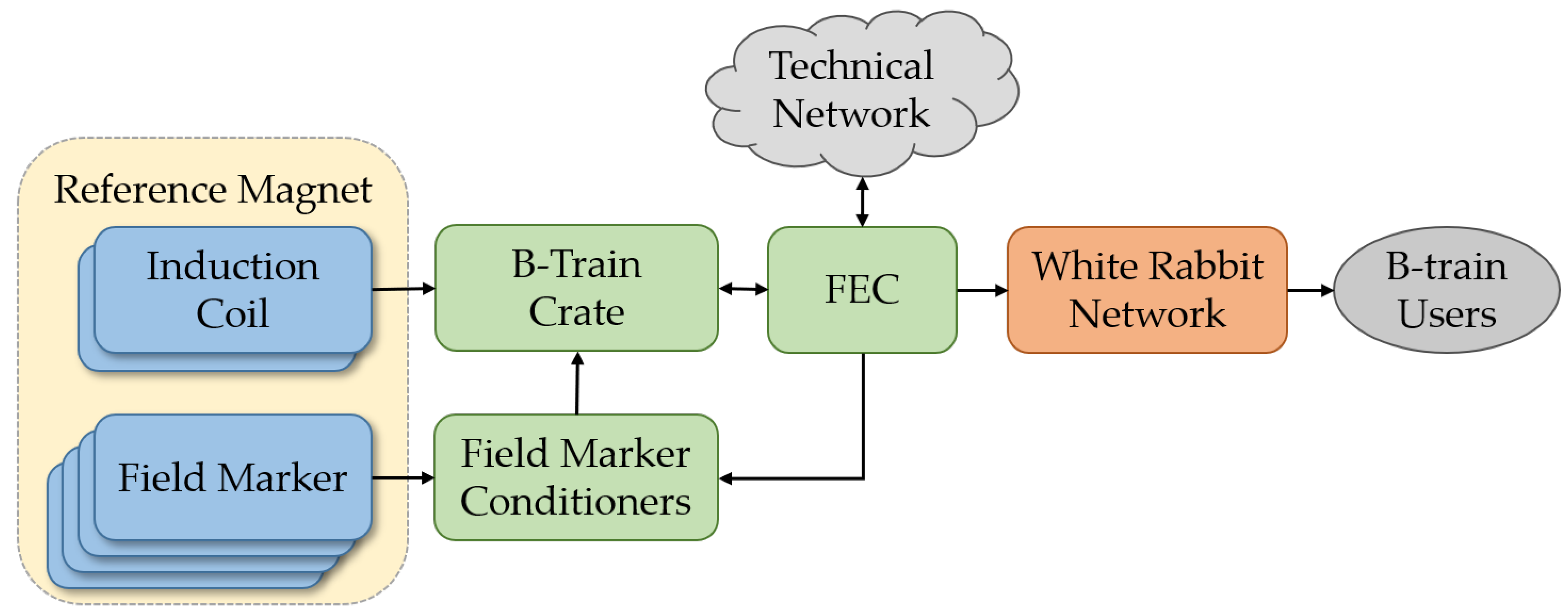
Figure 5 shows the architectural layout of the new system. Unlike previous ones, which contained a large number of custom components with many slight differences, FIRESTORM adopts a modular architecture based upon common hardware and parametric firmware. This implementation allows for each setup to be adapted efficiently based on the different sensor configurations required by the synchrotrons. The simplest case is the SPS B-train, where a long integral coil with one low-field marker provides input to a single integration channel. The ELENA system has also one integral coil but two field markers, each used on different magnetic cycles: a high-field marker for cycles where antiprotons are decelerated and a low-field marker for special test cycles that accelerate protons and H ions (in both cases, the marker is triggered just before injection). Yet another example is given by the combined-function PS magnets; these consist of two halves: one with a focusing and the other with a defocusing gradient, which must in principle be treated as two independent magnets. As such, each half requires a dedicated coil and integration channel. At present, the configuration has only one low-field marker implemented on each channel. Nevertheless, the system allows for the addition of a second pair of high-field markers, which, in upcoming operating scenarios, will be triggered sequentially on the same magnetic cycle in order to achieve higher accuracy both at beam injection and extraction.
A flexible architecture is therefore necessary to deal with these different requirements effectively, as well as the adaptations and improvements that we anticipate during the 20- to 30-years lifespan of the system. The modular approach taken by the design, together with the remote configurability and diagnostics capabilities made possible by the tight integration of the software within the site-wide accelerator control system, is expected to improve both the maintainability and longevity of the system.
The key functions of the FIRESTORM B-train are implemented by a set of modules based upon off-the-shelf PCIe FPGA carrier cards (Simple PCI Express Carrier, or SPEC) hosted in an industrial Front End Computer (FEC). Each SPEC card hosts a custom-made FPGA Mezzanine Card (FMC) that implements analogue and digital I/O. This architecture allows splitting out the different functions with a fine level of granularity, improving both the flexibility and the maintainability of the final system. All design elements, including PCB layouts and firmware, are released on the Open Hardware Repository (OHWR) [26], a CERN initiative aimed primarily at the High Energy Physics community to stimulate collaboration, as well as the commercialization of the designs by industrial partners. These cards are linked to the magnetic sensors through the B-train crate, acting as a central hub. The final design element is a fibre-optic Ethernet-based network called White Rabbit (WR) [27], which is used to distribute the measured field with high speed and noise immunity [28]. The use of an Ethernet frame allows for the transmission of the measured magnetic field alongside various ancillary signals, metadata and, crucially, three other versions of the field itself. These are: the field measured by the legacy system, where available; a copy of the nominal field obtained from the magnetic cycle database (simulated field, see Section 4.4); and a mathematical model of the field based on the magnet excitation current (predicted field, see Section 4.5. This is currently only at the prototype stage and is not implemented in the deployed systems). Access to these high-resolution, synchronized versions of the magnetic field is expected to greatly facilitate system diagnostics and to enhance operational flexibility in certain situations, e.g., when the measured field is not the most appropriate feedback source for the users (see Section 4.4).
In the following subsections, we describe in detail the design and function of all system elements.

3.1. Front End Computer and Software

The core of the FIRESTORM system is the FEC, shown in Figure 6, an industrial diskless rack-mounted PC hosting the main electronic components [29]. About 2000 FECs are deployed throughout CERN for interfacing with devices that are involved in synchrotron control, such as RF and vacuum control systems, beam diagnostics instrumentation as well as the B-train systems. The current generation of FEC is the Siemens SIMATIC IPC847E with up to 11 free PCIe slots. The operating system is 64-bit CentOS7 Linux [30], and the software is based on a distributed, real-time C++ class framework called Front End Software Architecture (FESA), which is at the heart of accelerator controls at CERN and GSI [31]. FESA abstracts the interface between the high-level accelerator control infrastructure and the local hardware, which is accessed via user-written device drivers. Tools are provided to help with the generation and debugging of C++ code. Automatic mechanisms are provided to store and retrieve class properties representing configuration parameters from a common database, as well as broadcasting measurement and diagnostic data vectors across the complex in quasi-real-time, i.e., with a latency of the order of a full magnetic cycle, which is adequate for many non-critical tasks. All communication happens on the Technical Network, a segregated Ethernet network secured against intrusion that is used to control and monitor all accelerator systems.
FESA is tightly integrated with the hardware timing system, which is used to synchronize the accelerators and their subsystems within a few microseconds [32]. This system consists physically in a network of coaxial cables, independent for each accelerator, distributing several hundreds of trigger pulses that represent timing events relevant for beam or equipment monitoring and control. A separated serial channel for each accelerator (the so-called Machine Telegram) distributes information, including the type of magnetic cycle being run, the destination of the beam and the type of the next synchrotron cycle that will be run. The framework has recently been fully endowed with so-called Pulse-to-Pulse Modulation (PPM) capabilities, which enable or disable specific actions, such as class property setting and broadcasting, according to cycle type. PPM is a novel, crucial functionality that allows for the automatic adaptation of sensor calibration parameters to the magnetic characteristics of the synchrotron cycle; in particular, this applies to the field marker level B m , which for the best accuracy should be calibrated independently for each cycle type. Compared to the manual updating carried out in the older B-train systems, this mechanism dramatically improves the flexibility and reliability of the configuration process. At present, the FIRESTORM FESA software comprises four different classes: the B-train class, which interfaces with all sub-systems that produce the measured field B ¯ ; the FSBT_BTG class, specifically for controlling the simulated field; the CosmosCheckWRS, which monitors the status of the White Rabbit network; and the Comet_EVM for environmental monitoring. Altogether, the FESA framework allows for the adjustment of more than 200 different configuration variables, inherent to the operation of the B-train, as well as access to over a 100 acquisition parameters, including internal registers and measurement values.

3.2. SPEC—Simple PCIe Carriers

The SPEC (see Figure 7) is a general-purpose FMC carrier card with ready-made drivers ("spec-sw" on OHWR) that encapsulate the complexity of the host bus communication protocol, thus greatly simplifying the whole development cycle [33]. Several bus variants are available on the market, including VME, PXIe as well as PCIe interfaces, along with various types of FPGA modules.
The 4-lane PCIe version implemented in the FIRESTORM B-train is based on a 250 M Hz Xilinx Spartan-6 LXT FPGA [34], offering 101,261 logic cells and 4 . 824   k b memory. Currently, at most, 50% of the gate resources are used up in any module, which leaves considerable room for future improvements. The FPGA implements a finite state machine that defines the logical behaviour of each component and a number of DSP cores that carry out the real-time signal processing tasks in 32-bit fixed-point representation (matching the WR distribution data format). Additional connectivity features include a Small Form-factor Pluggable (SFP) fibre optic port that can be used for WR distribution (see Section 4.6), a low-pin count connector (LPC) as the FMC interface, plus standard SATA, mini-USB and JTAG (for FPGA programming) connectors.
The internal memory structure of the FPGA and its external interface are defined with the help of Wishbone, an open-source core-to-core logic bus [35]. A tool (wbgen2 on OHWR [36]) is available to generate semi-automatically VHDL or Verilog cores that implement registers, memory blocks, FIFOs and interrupts, along with the corresponding C header files. In this way, FESA software components can easily access and manipulate related variables and data structures. In particular, the transfer of large memory blocks representing the waveforms of various acquired or processed data is transferred via DMA through the PCIe bus to be broadcasted across the network. We note that, in the current implementation of the system, only one SPEC card at a time is allowed to have DMA to ensure stability. All the basic functionalities of the SPEC, including configuration, initialization, etc., are managed automatically by the FESA framework.

3.3. FMC—FPGA Mezzanine Cards

The FIRESTORM B-train design includes four different types of FMC conforming to the FPGA Mezzanine Card ANSI/VITA 57 standard [37], which decouples I/O functions from the FPGA and allows simpler, modular designs. Except for the CERN-standard Central Timing Receiver (CTRI) card, which realizes the interface to the timing system, the other three cards were developed for the specific functions of the field marker trigger generator, magnetic flux integrator, White Rabbit I/O, simulated and predicted field features, all described in detail in Section 4. The last three functions require no specialized hardware, so they share the same FMC card design. The FMC designs are based on a small form factor that connects to the FPGA via a 160-pin LPC interface, which allows a theoretical bandwidth up to 40 G / s with negligible latency and no protocol overhead. The major drawback of this choice is the difficulty of transmitting clock signals from the carrier to the mezzanine, thus preventing true hardware synchronization between the different cards. At present, this does not represent a limitation, as the overall latency meets the requirements (see Section 6.2). Both the integrator and trigger generator FMC cards implement small-footprint, ultra-low phase noise Crystek CCHD-575 oscillators to generate locally a 80 M Hz clock with ± 20 ppm worst-case frequency stability.
Communication between the FMC cards, the B-train crate and the WR transmitter is provided by a daisy chain of standard HDMI cables with 19-pin mini-HDMI connectors, chosen for their small size and robustness. Each HDMI cable carries a 250 M Hz Low Voltage Differential Signal (LVDS) link, which allows bi-directional, self-clocked Manchester-encoded serial transmission with a theoretical 250 M b / s throughput. Transmission latency is typically less than 1 μ s , mainly due to the serialization/serialization steps. In parallel, eight conductors are dedicated to differential 2.5   V logic Digital I/O (DIO) channels, which allow the relaying of various kinds of trigger pulses with no protocol overhead.
An important goal of the LVDS links is to convey the different versions of the magnetic field to the White Rabbit frame assembler (see, Section 4.6), bypassing the PCIe bus with its associated programming complexity and uncontrolled latency. The daisy chain starts with the integrator module (which was the first component to be designed during the development phase), proceeds through the Simulated Field module and terminates at the WR transmitter. As discussed in Section 6.2, this arrangement results in a slight increase in the overall measurement latency while still remaining acceptable. A separate LVDS link allows the direct exchange of data between the integrator and the trigger generator card.

3.4. B-Train Crate

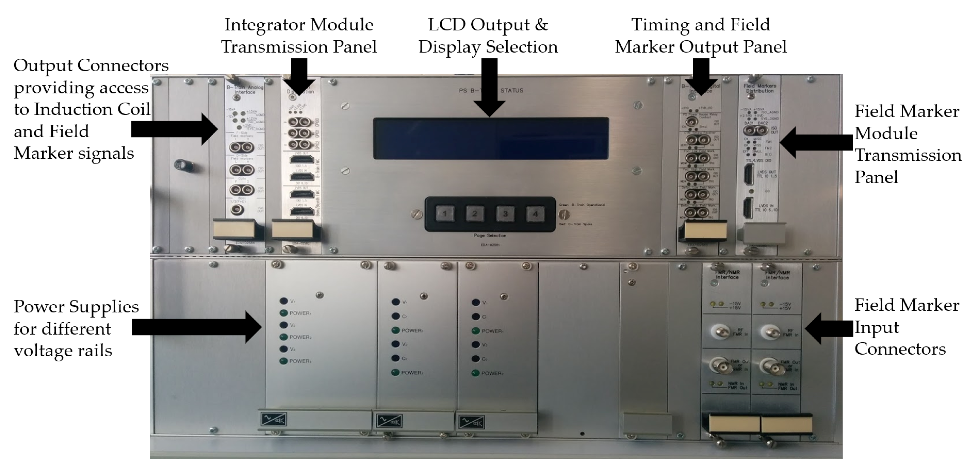
The B-train crate, as shown in Figure 8, is the external interface of the FIRESTORM system, working as a hub for routing internal and external signals. The crate includes analogue and digital interface modules that allow local diagnostic access to all sensor outputs, the field marker triggers as well as the distributed magnetic field. In particular, a module is designed to accept the incremental pulse distribution of the legacy B-trains as input based on two parallel 24 V pulse trains, which represent, respectively, ± 10   μ T field increments, accumulate the field value it and send via LVDS to the Integrator module for inclusion in the output stream.
The analogue outputs are duplicated on the back-plane of the crate in order to feed OASIS, a distributed acquisition system that allows monitoring, with some bandwidth and resolution limitations, all of CERN’s operation-related equipment signals [38]. The front panel hosts a set of HDMI connectors that allow to make the links between the FMC cards or to break them to access individual signals for diagnostics. Finally, a large LCD multi-screen panel is provided to display real-time status information, such as the measured field B ¯ , sensor calibration parameters and other FPGA registers.

4. Functional SPEC Modules

In this section, we describe in detail the design and functions of the six kinds of SPEC/FMC modules used in the FIRESTORM B-train.

4.1. Central Timing Receiver

The Central Timing Receiver card is a CERN-standard component installed in all FECs, where it receives and decodes General Machine Timing (GMT) events that contain information on the cycle being performed in each accelerator [39]. The FIRESTORM system utilises the CTRI for generating two critical local timing TTL triggers:
  • the “C0” trigger, which signals the start of a new accelerator cycle and is used as an internal reference for various time-related functions, such as the integrator calibration procedures and the field marker gating function described below. Optionally, C0 can be used to enforce a restart of the flux integration process to a given preset value. This is useful, for example, when a field marker malfunction is suspected.
  • the “ZERO” cycle trigger, which signals the start of special cycles where no beam is circulating, and the magnet excitation current is kept at a low (or zero) level. ZERO cycles are run from time to time in some (but not all) of CERN synchrotrons, either as low-power fillers in the machine schedule or to allow capacitive-discharge magnet power supplies time to recharge. Whenever available, ZERO cycles are used for self-calibration of the integrators, as described in Section 4.3.
These triggers are distributed through standard coaxial cables to the B-train crate, where they are first converted to 2.5   V pulses and then relayed to the integrator and the other FMCs via the HDMI DIO lines.

4.2. Field Marker Trigger Generator Module

The Field Marker Trigger Generator module has the goal of detecting the resonance peak in the output V m of an NMR or FMR resonator and to generate a TTL trigger pulse accordingly. The module has a dual-channel design that allows, for example, having a high-field and low-field marker acting at different times on the same integration channel (as in ELENA [7]) or two markers acting in parallel on two separate integration channels (as in the PS). We recall that the B-train crate has a number of connectors sufficient to handle up to four field marker signals, corresponding to up to two SPEC/FMC cards operating in parallel in the same FEC. The field marker output is initially routed through a signal conditioner board in the B-train crate. This removes the DC component, allowing for the subsequent comparison to a known threshold and then optionally amplifies the signal (this is necessary only for the FMR sensor, not the NMR) [20]. In the following, we describe in detail the hardware of the Field Marker FMC and the peak detection algorithm implemented in the FPGA.

4.2.1. Field Marker FMC

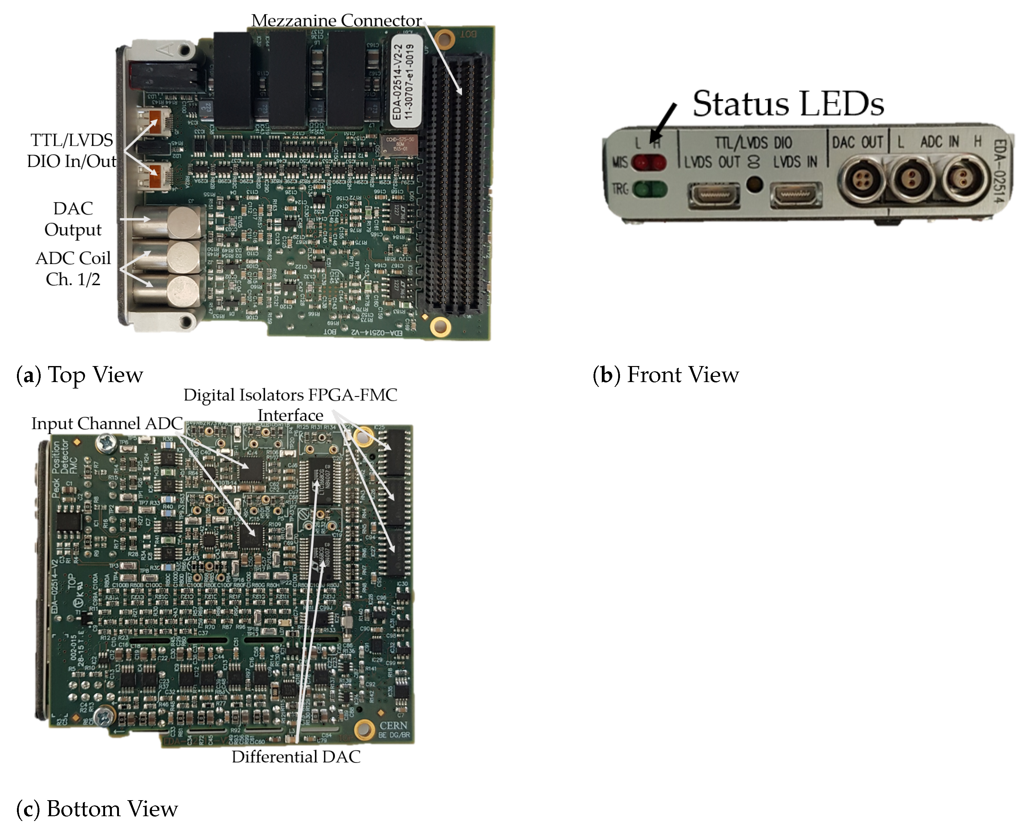
The Field Marker FMC (EDA-02514, see Figure 9) includes two fully independent, parallel acquisition channels based on a 16-bit, 10 MSamples / s AD7626 ADC with a ± 4   V differential input range. The analogue input stage includes a low-pass filter that is essential for removing the noise generated by the sensor or picked up along the way, thus avoiding spurious triggers. The cut-off frequency is usually set around 2 k Hz , which corresponds to a detection delay of the order of 100 μ s ; being systematic, this has negligible impact on the calibration of B m , at least as long as the field ramp rate at the time of triggering is constant [22]. No additional anti-aliasing filter is necessary.
I/O connectors include dual LEMO inputs for analogue field marker signals, a LEMO analogue output for the on-board DAC and two mini-HDMI sockets for the input and output LVDS DIO. The generated 1 m s trigger pulse is transmitted on the LVDS output to the Integrator module, from which it is propagated down to the WR module to be written into the distributed WR Ethernet frame (see Section 4.6). In addition, we find four diagnostic status LEDs that signal, on any given machine cycle, the detection of the high- and low-field marker triggers or the lack thereof within the allowed time window.

4.2.2. Peak Detection Algorithm

The resonance peak is defined as the first zero-crossing of the derivative of V m and the corresponding time t * = t j is defined by:
j = m i n ( i ) : t 1 t i t 2 | V m , i | V ¯ s i g n ( V ˙ m , i ) s i g n ( V ˙ m , i 1 ) ,
where i is the running index of the waveform samples; [ t 1 , t 2 ] is a pre-defined gating window, typically 20 m s long, that prevents spurious triggers to happen too far from the expected time during a cycle; V ˙ m is the time derivative of the sensor output, calculated with a seven-point finite-difference scheme; and V ¯ represents a voltage threshold, set independently for each system above the residual noise level after filtering. As the zero-crossing can happen anywhere within the [ t i 1 , t i ] interval, this simple algorithm has an uncertainty of ± 50   n s , which is negligible. We recall that all the algorithm’s parameters are stored in FPGA registers loaded at run time by the FESA software, which can be adapted automatically to the type of cycle being run via the PPM mechanism.

4.3. B-Train Integrator Module

The dual-channel B-train Integrator module has the primary role to determine the value of the average field B ¯ that is distributed to the B-train users. In addition, it has the capability of accepting the incremental pulse distribution of the legacy B-trains as input based on two parallel 24 V pulse trains that represent, respectively, ± 10   μ T field increments, to accumulate it and to distribute the result alongside the FIRESTORM measurement. The main issue affecting this measurement is the drift caused by a voltage offset δ V superposed to the coil output V c . We observed that the offset has a spectrum akin to 1 / f pink noise, with a slowly drifting, almost systematic component superposed to random fluctuations with periods of the order of a few seconds to a few minutes, comparable with the duration of most accelerator cycles [40]. Such an offset can be mitigated, for example, by choosing high-quality discrete components causing imbalances in the analog input stages, by reducing thermal gradients leading to thermoelectric voltages and, in general, by ensuring long-term thermal stability via adequate ventilation. With respect to other voltage integrators described in the literature [3,12,41], the specificity of our design lies in the method used to estimate it and correct in real-time. For simplicity, we assume that throughout each integration interval (or, equivalently, accelerator cycle), δ V is a constant and re-evaluate it periodically. In the following subsections, we discuss in detail the hardware of the mezzanine card, the integration and error correction algorithms.

4.3.1. Integrator FMC

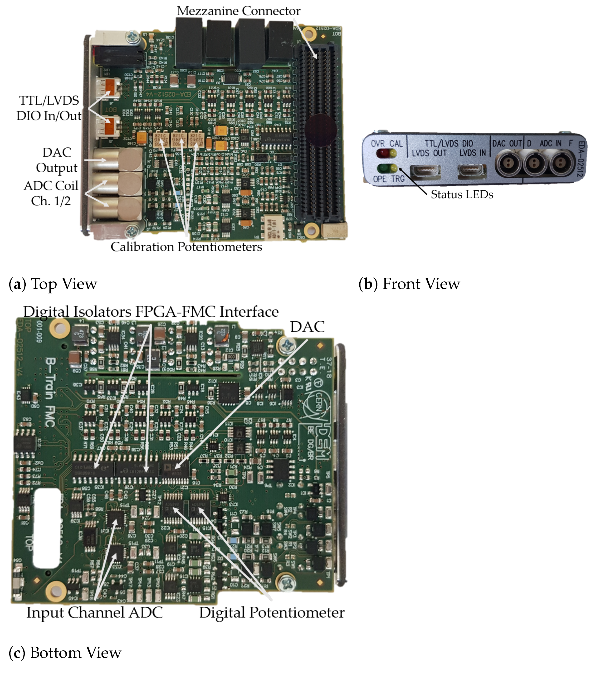
The Integrator FMC (EDA-02512) is shown in Figure 10. The core of each FMC integration channel is a high-linearity 18-bit, 2 MSamples /s AD7986 SAR ADC with a 0 V – 5 V differential input range. Each channel includes the following conditioning stages:
  • A three-way selection switch with a 200 μ s settling time for the auto-calibrating function, as explained below.
  • An input buffer with a 27 M Hz bandwidth and a R in = 2 M Ω impedance. The impedance stems from a compromise between the need to limit signal attenuation for high-resistance input loads and the need to limit the offset voltages arising due to input bias currents. For a typical measurement coil resistance on the order of R c = 1 k Ω , the low-frequency attenuation can be easily calculated from R c R c + R in 500 ppm and corrected in the post-processing stage. As the specified input signal bandwidth is just 100 Hz , a more rigorous dynamic study of the parasitic capacitive effects was not considered a priority at this stage.
  • A two-stage pre-amplifier that scales the nominal ± 10   V induction coil signal to the ± 5   V differential input range of the ADC. First, a voltage divider realized with high-precision discrete resistors attenuates the signal by a factor of 5 / 8 ; then, a fully differential funnel amplifier AD8475 with the attenuation factor is 4 / 5 and nominal passband 15 M Hz prepares the signal for the ADC while ensuring that the total attenuation factor is 1 / 2 .
  • An AD5291 digital potentiometer providing a programmable voltage source with 1 m V range and about 1 μ V resolution, injected between the two attenuation stages and used for fine offset compensation.
  • A simple first-order RC anti-aliasing filter with a 1 M Hz cutoff frequency, which gives a nominal 100 ppm maximum error at the upper end of the 100 Hz signal bandwidth.
The board includes also a multi-purpose AD5791 DAC with a ∼ 1 μ s settling time, whose output can be applied to the integrator input by switching the input selector to the position 2, as shown in Figure 11. This is used both for the periodic gain self-calibration and to generate various kinds of analogue output signals as may be needed for diagnostics (e.g., an image of the measured field B ¯ to be visualized on the spot with an oscilloscope) or for special purposes (e.g., an image of the field derivative B ¯ ˙ that is used to compensate eddy current effects in the PS magnets). Three mechanical potentiometers are also included to adjust manually the offset, positive and negative range of the DAC as needed for gain calibration, as explained below. I/O connectors include, besides the dual ADC input and the DAC output, two TTL/LVDS DIO connectors for the daisy chaining and diagnostics of the card’s output. Finally, four diagnostic status LEDs signal, on any given machine cycle, the reception or lack thereof of a high- or low-field marker trigger.

4.3.2. Integration Algorithm

The integrator implements two identical acquisition and computation chains in parallel, which are combined linearly to provide the final output:
B ¯ = k 1 B ¯ 1 + k 2 B ¯ 2 .
This implementation provides the flexibility to use only one set of sensors or to mix two sets according to the circumstances, as is required, for example, in the PS B-train system. In the following, we describe in detail the operation of a single channel, dropping for simplicity the index from all related variables. The data-flow is represented schematically in Figure 11, where the analogue pre-processing and signal digitization performed by the FMC is on the left, while the numerical processing carried out by the FPGA is on the right.
In our calibration model, we assume that the differential voltage Δ V in at the input of the conditioning stage is the sum of the coil output voltage V c and the offset δ V :
Δ V in = V c + δ V .
In other words, we only consider the sources of offset internal to the card (e.g., due to discrete component imbalances) and neglect the external ones, such as thermoelectric gradients on the cabling between the induction coil and the card. This approximation is usually sufficient to obtain good results, as shown in Section 5.3.
The differential voltage Δ V in at the input of the ADC can be expressed as:
Δ V in = 0.8 0.625 Δ V in + Δ V 2 = 1 2 Δ V in + 4 5 Δ V 2 ,
where Δ V 2 is the programmable offset added by the digital potentiometer. The sampled voltage is first corrected according to Equation (8):
V out = G cc V ADC + Δ V 1 ,
where G cc 1 is the internal gain correction factor, and Δ V 1 represents the coarse offset correction. To remain within the FPGA resource limits with a reasonable margin, all variables in Equation (8) are represented in 18-bits, with an effective resolution of 1 LSB 76 μ V . The change in magnetic flux Δ Φ is integrated according to:
Δ Φ i = τ s j = i k * i V out , j ,
where j is a running sample index, i k * marks the start of the current integration interval upon reception of the k-th field marker trigger, and τ s = 500 n s is the sampling time. The calculations in Equations (8) and (9) are carried out with a 56-bit depth to avoid overflow, and the flux change Δ Φ i is represented with a depth of 32-bits ( 1 LSB 5 n V s ) to match the format of the final output. Finally, the average magnetic field is computed according to Equation (10):
B ¯ i = γ ( B m α Δ Φ i A c ) ,
where the non-dimensional coefficients γ and α represent correction factors, accounting, respectively, for the difference between the reference magnet and the average of those in the accelerator and any error in the effective area or the position of the coil, as discussed in [14].

4.3.3. Drift Correction

Drift correction relies on the availability of beam-less ZERO cycles during which the integrator input can be safely short-circuited (position 3 of the input switch in Figure 11), and the observed drift can be attributed entirely to the voltage offset δ V. Since sometimes the accelerators operate with many, closely spaced ZERO cycles, we impose a dead time of 5 minutes between corrections, which, in practice, was found to help us avoid possible instability. During the correction process, the distributed field values will of course be meaningless and must be disregarded by the users; in particular, the power converters feeding PS and PSB magnets must open their control loops to avoid runaway instability.
The estimation and compensation of the voltage offset are carried out in two stages. The first stage is purely numerical and occurs in the FPGA, where the coarse offset correction Δ V 1 is derived by averaging the voltage during a portion of a ZERO cycle:
Δ V 1 = δ V = Δ Φ 0 n 0 τ s = 1 n 0 i = i 0 i 0 + n 0 1 V out , i ,
where the index i 0 marks the start of the short-circuit measurement, n 0 represents its duration in samples, and Δ Φ 0 is the measured flux drift. The duration of this measurement should be as long as possible to improve the accuracy of the computed average, which scales as n 0 1 / 2 ; however, it is important to leave some margin at the start of the cycle for the control loop of the power converters to be opened. As an example, in the PS system, we set i 0 = 400 k S or, equivalently, 200 m s after C0 and n 0 = 200 k S , corresponding to a 100 m s duration.
Since the resolution of Δ V 1 is limited to 1 LSB = 76 μ V , we decided to implement an additional correction stage, adding a much finer offset Δ V 2 to the signal in the analogue input stage. This offset can be set with a 1 μ V resolution over a range of ± 500   μ V . Different strategies are currently being evaluated to set an optimal Δ V 2 , including differentiation followed by low-pass filtering of the measured flux or an iterative binary search strategy that aims at zeroing the measured drift. As this feature is still at the prototype stage, all the results reported in Section 5.3 have been obtained by setting Δ V 2 = 0 .

4.3.4. Gain Correction

The linear gain correction procedure is also performed during a ZERO cycle immediately after the offset calibration described above, except that the input is switched in position 2 of Figure 11. This applies to the input of the acquisition chain and the output of the high-precision DAC, used as a voltage reference in the range between ± V ref , with V ref = 8.75   V . In this range, which covers the majority of cases, the DAC shows a very good linearity; moreover, V ref has an exact hexadecimal representation in the VHDL code, which improves the accuracy of the gain correction. The DAC itself is calibrated manually at least once, as part of the production tests, with an external Agilent 34401A multimeter [42]. The three mechanical potentiometers installed on the FMC are used, respectively, to remove first any offset at 0 V and then to adjust the values of ± V ref . This calibration procedure can be repeated during operation if deemed necessary. The gain correction procedure consists of applying to the input first + V ref and then V ref , over two sequences of n 1 samples each, during which the FPGA computes the average of the sampled voltage. Taking into account the scaling done by the conditioning module in Equation (7), the gain correction factor is then computed as:
G cc = 1 2 V ref 1 n 1 i = i 1 i 1 + n 1 1 V i 1 n 1 i = i 2 i 2 + n 1 1 V i 1 ,
where i 1 = i 0 + n 0 + Δ n is the starting sample of the + V ref acquisition, Δ n = 1 kS is an interval of 0.5   m s introduced to give the input time to stabilize, n 1 = 300   k S corresponds to the duration of the acquisition of 150 m s , and i 2 = i 1 + n 1 + Δ n is the starting sample of the V ref acquisition.

4.4. Simulated Field Module

The simulated field module, schematically represented in Figure 12, generates a high-resolution image of the nominal, pre-programmed magnetic cycle in real-time as it is stored on the centralized LHC Software Architecture (LSA) database [43]. The role of this feature is twofold:
  • As a normal part of the accelerator restart sequence, when the accelerating RF cavity control system needs a realistic value of the field to be input via the B-train for its own frequency program, even when no beam is circulating yet and the magnets are not powered.
  • Under certain special circumstances, when the magnetic field measurement feedback is not the best option. For instance, machine operators may want to replace the measured field temporarily with the simulated one as a beam diagnostic tool. As another example, in the case of a power converter trip, the value fed back to the RF cavities must switch automatically from the measured to the simulated field in order to avoid large, potentially harmful discontinuities. Even more crucially, in the specific case of the AD, the simulated field is always preferred because the machine is magnetically very reproducible, and the RF system is adversely affected by the noise inherent in the measured field.

4.4.1. Vector Cycle Representation

The image of each cycle is stored in the LSA as a two-column vector table, where the first column represents time and the second, in general, the magnetic field. One exception to this rule is provided once more by the AD, where the LSA image contains the magnet excitation current waveform, and the B-train software must apply a given analytical relationship to derive the magnetic field. (This involved procedure is not necessarily more precise than a measurement, but the accelerator was finely adjusted accordingly in the 1990s, and today, there is hardly reason to change).
The vector cycle representation is very compact, with most cycles being described accurately by a few dozen to a few hundred vectors. A finer resolution is generally required at high field, where the current-to-field relationship is non-linear due to iron saturation, or to smooth out discontinuities at the junction of current ramps and plateaus. A maximum number of 7025 vectors can be accommodated in the SPEC’s on-board RAM, which is more than enough for any present or anticipated need. A small memory footprint is also critical to pre-fetch the table quickly from LSA for the next cycle while the current cycle is still running. The telegram provides an advance of at least 1.2   s , i.e., one basic accelerator period, which is largely sufficient for the FESA software running on the FEC to interrogate the database, download the data via the Technical Network and transfer it onto the Simulated Field card. (By default, all external data is transferred onto the Integrator module via PCIe DMA, and from there it gets handed to the other modules down the LVDS daisy chain. The only exception to this is the AD system, where there is no Integrator module and DMA is implemented directly in the Simulate Field module FPGA). This new strategy, unlike the legacy B-train systems, which kept in memory the full high-resolution time series corresponding to a few cycle types, is way more efficient and general as it can adapt transparently to any of the thousands of cycles already stored or expected in future.

4.4.2. Magnetic Cycle Interpolation

The table of vectors is interpolated to the desired resolution (by default, 4 μ s ) in real-time in the FPGA using Bresenham’s line algorithm. Practical details are different, according to the accelerator. Implementation is simpler for the accelerators in the PS complex (LEIR, PSB and PS), where the cycle length can only be one, two or three basic 1.2   s periods. Conversely, in the antiproton decelerators (AD and ELENA), cycle vectors are not necessarily known a priori but are defined at run time by specific start and stop timing events, triggered manually by operators in the Control Room. This mechanism provides the possibility to prolong a plateau for an arbitrary duration, up to a couple of minutes, as required for beam electron cooling or to accumulate antimatter for various experiments. During these pauses, the interpolation is temporarily stopped and the B-train outputs a constant value. The possibility of pausing a cycle on the flat-top by means of a specific set of timing events is also implemented in the SPS, where it used to adjust beam extraction for ion-beam momentum slip stacking [44].

4.4.3. Simulated/Predicted/WR FMC

The FMC of the Simulated Field module (EDA-03557), which is physically the same for the Predicted Field and WR modules, is shown in Figure 13. On it, we find two input and two output mini-HDMI connectors for LVDS DIO: one SFP optical port for WR and one coaxial output for the on-board AD5791 DAC.

4.5. Predicted Field Module

The Predicted Field module, which at the time of writing is at an early prototype stage, implements a mathematical model to derive the magnetic field in real-time from the excitation current. This can be useful in a variety of scenarios, which overlap with the Simulated Field use-cases. For example, machine operators might want to switch temporarily from the measured to the predicted field as a diagnostic measure, whenever they suspect a sensor malfunction; or, the difference between measurement and expectation can be continuously monitored as a powerful real-time diagnostic tool. In the long-term, if proven to be sufficiently accurate, the prediction might replace the measurement altogether, drastically cutting the cost and complexity of the future B-train system.
Different categories of mathematical models are being considered as candidates for this functionality. At CERN, a semi-empirical analytical model called FIDEL [45] has been used with success since 2007 to derive offline the inverse field-to-current relationship of the superconducting LHC magnets, as needed for open-loop control with 100 ppm accuracy. This is possible thanks to the coil-dominated character of these magnets and to the very high field they reach, well above 8 T , which minimize the impact of non-linear effects, such as iron saturation, hysteresis and eddy or persistent currents. In the iron-dominated magnets below 2 T , such as those found in all other accelerators at CERN, these effects can affect the magnetic field much more severely, which makes the task more challenging.
This is especially true for history-dependent features, such as the remanent field or the response to minor hysteresis loops, as illustrated by the failure of an early linear dynamic model tested in the PSB [46]. Different classes of hysteresis models are discussed widely in the literature, including closed-form or differential analytic expressions, operator-based and neural network formulations, which have had some success, such as those in [47]. At present, these are still being evaluated to identify the most suitable one for real-time FPGA implementation.

FMC

The Predicted Field FMC carries no specialized hardware and is indeed the same as the one for the Simulated Field described above. The FMC can accept as an input the current measured with a high-precision Direct Current to Current Transformer (DCCT) and distributed by the controller of the power converters over a dedicated WR network, using a specific definition of Ethernet frame that also includes the status of the power supply and its output voltage. The frame rate, in this case, is much lower than for the B-train WR, i.e., usually 10 kfps , which corresponds to the operational frequency of the digital controller of the power converter.

4.6. White Rabbit Module

White Rabbit, adopted as the IEEE 1588-2019 standard, is an Ethernet-based network for real-time, large-scale distributed control systems, featuring deterministic data delivery at gigabit speed with sub-nanosecond synchronization over multiple kilometers of optical fiber [28]. Originally developed at CERN, it is now openly accessible under the GNU general public license in the OHWR and is supported by National Instruments and many other vendors. Given the tight timing constraints and the requirement to distribute the actual value of the magnetic field serially, rather than just the increments as in the old systems, WR was a rather natural choice [48]. The added value of this solution resides in the improved maintainability of the network based on commercially available routers and switches. These components can be remotely configured and upgraded with a full suite of powerful remote debugging and diagnostic facilities that allow for the measurement of the transmission latency, warn of packet loss and more.
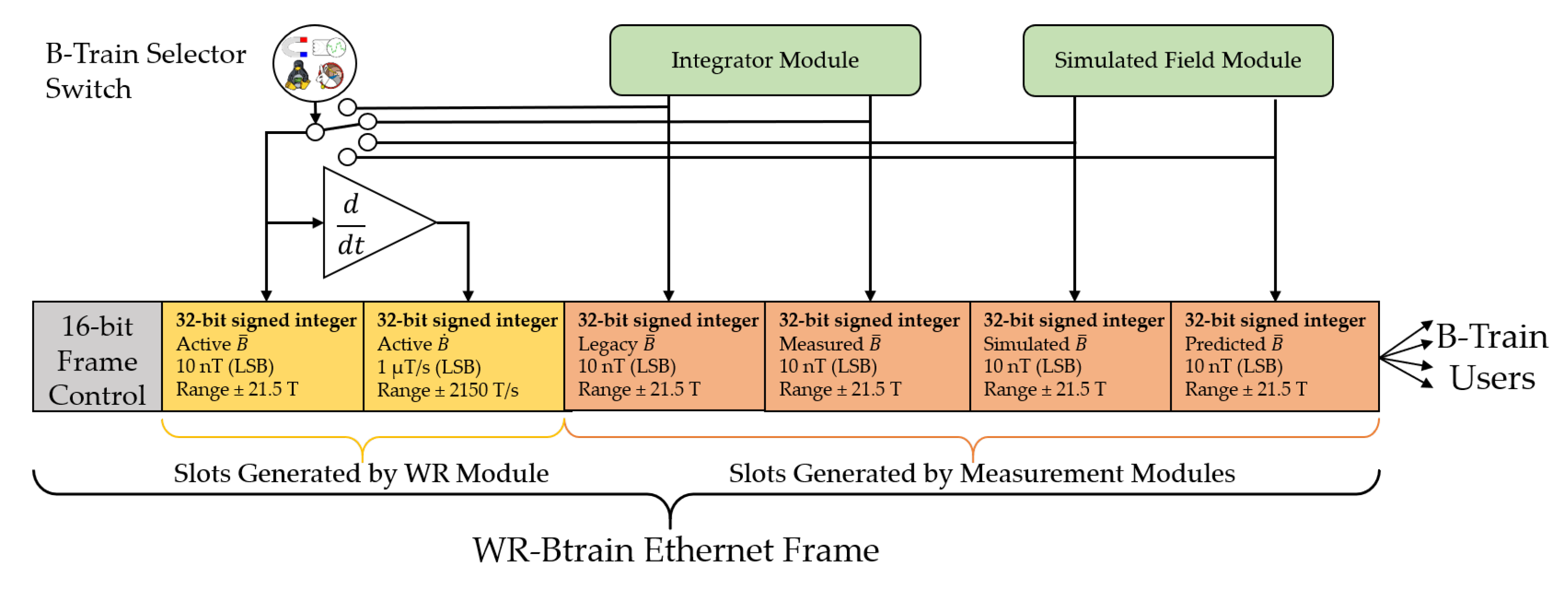
The measured, legacy, simulated and predicted fields are distributed through the LVDS daisy chain connections to the WR FMC card, which is physically identical to those of the simulated and predicted modules. The FMC offers physically the possibility of being used either as a receiver or a transmitter, the actual functionality being implemented in the SPEC gateware. In the FIRESTORM B-train, the FPGA handles the task to assemble the data in the so-called WR-Btrain frame, illustrated in Figure 14. The B-train frame is 26 bytes long and includes, in this order:
  • A 16-bit frame control header, consisting of an 8-bit frame type ID and various status and error flag bits, essential for remote diagnostics and calibration. In particular, there is a flag bit that signals if the current cycle is a ZERO cycle; and two additional flag bits, which are set to 1 to indicate the reception, respectively, of the C0 (cycle start) and field marker trigger pulses. Since the pulses have a nominal width of 1 m s , each one of these two flags will normally be set on 250 consecutive frames.
  • The first part of the payload, comprising two 32-bit slots for the active B ¯ and B ¯ ˙ values. The active version of the magnetic field is selected among the four possibilities and is positioned in the first slot to ensure that all users read by default the same value. In signed fixed-point representation, the distributed field has a resolution ( 1 LSB) of 10 n T and a range of ± 20   T , which is more than enough for all foreseeable applications. The second slot contains the numerical time derivative of the first one, with a resolution of 1 μ T / s and a range of ± 2   k T / s , also exceeding all foreseeable demands.
  • The second part of the payload, which includes four 32-bit slots for the measured, legacy, simulated and predicted field, with the same resolution as the active field slot. Repetition of the active field slot implies a redundancy of 4 bytes in the payload, which has negligible impact; in return, this guarantees that all users and diagnostic tools may conveniently access at any time the four versions of the field, at fixed slots within the frame.
The WR-Btrain frame is distributed as part of the larger streamer frame consisting of a 46-bytes payload, the minimum-length for an Ethernet frame. As padding is implemented to achieve the required payload size, this arrangement leaves five additional 32-bit slots free for future expansion [49]. Based on the frame size, this corresponds to a maximum theoretical rate of 1.4 Mfps over a gigabit optical link. At present, a steady transmission rate of 250 kfps is achieved reliably, while tests are ongoing to establish a practical upper limit.
To conclude, we remark that in the future, the same frame design could easily be adapted to distribute, in real-time, other multipolar field components in the accelerator ring, such as the gradient generated by the focusing and defocusing quadrupole magnets.

5. DC Performance

The accuracy of the integrator acquisition chain under DC input conditions has been evaluated by applying a known reference voltage to V in and comparing it to the measurement results. The voltage source used was a Data-Precision-8200 multifunction calibrator, which is characterised by a nominal resolution of 10 μ V and an output noise level of about 300 μ V RMS. A total of 20 values in the range between ± 8.75   V were applied sequentially, while at the same time, the DAC output was measured with an Agilent 34401A multimeter [42,50]. In the following, we discuss separately the results concerning voltage, magnetic flux and integrator drift.

5.1. Voltage Measurement

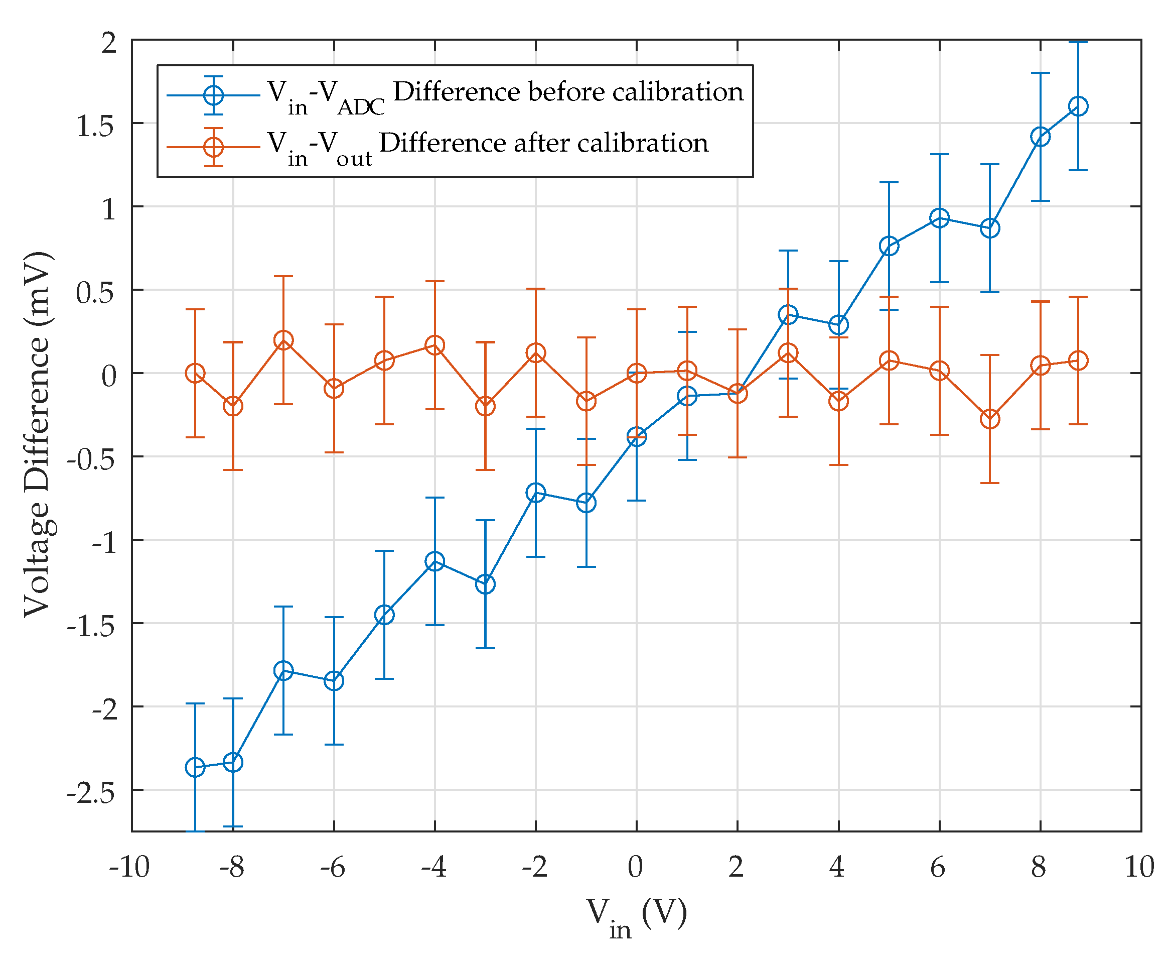
The accuracy of the voltage measurement, including the in-built gain and the coarse offset corrections, has been determined by comparing the known input with the values of V ADC and V out taken from the internal FPGA registers. During the tests, the fine offset correction Δ V 2 has been set to zero, and the results are plotted in Figure 15. The error bars represent the repeatability, σ V = 400 μ V , obtained from the standard deviation over 150 measurements, corresponding to about 5 LSB. For the most part, this scatter is due to the external source, as confirmed by performing the measurements with the input shorted, in which the intrinsic noise of the acquisition chain is about 100 μ V slightly more than 1 LSB.
The difference between V ADC and V in provides an indication of the error introduced by the conditioning and digitisation stages, which from Figure 15, is approximately linear. It can be seen in Table 1 that the slope and offset, as obtained from linear regression, are very close to the parameters determined by the in-built correction algorithms. Since these are more than one order of magnitude above the nominal ratings of the ADC, the error must be ascribed essentially to the analogue conditioning stage. From the difference between V out and V in , it is possible to determine the residual error following the in-built correction, which is random across the whole input range and has an RMS average of 135 μ V , i.e., a little less than 2 LSB.

5.2. Flux Measurement

The accuracy of the flux measurement has been determined by integrating a constant input voltage V in in the range ± V ref over a precisely set duration of Δ t = 1 s , taking a zero integration constant, and comparing the output Δ Φ , as read from the FPGA register, to the expected value V in Δ t . The results, expressed in terms of the equivalent voltage difference:
Δ V e = Δ Φ / Δ t V in ,
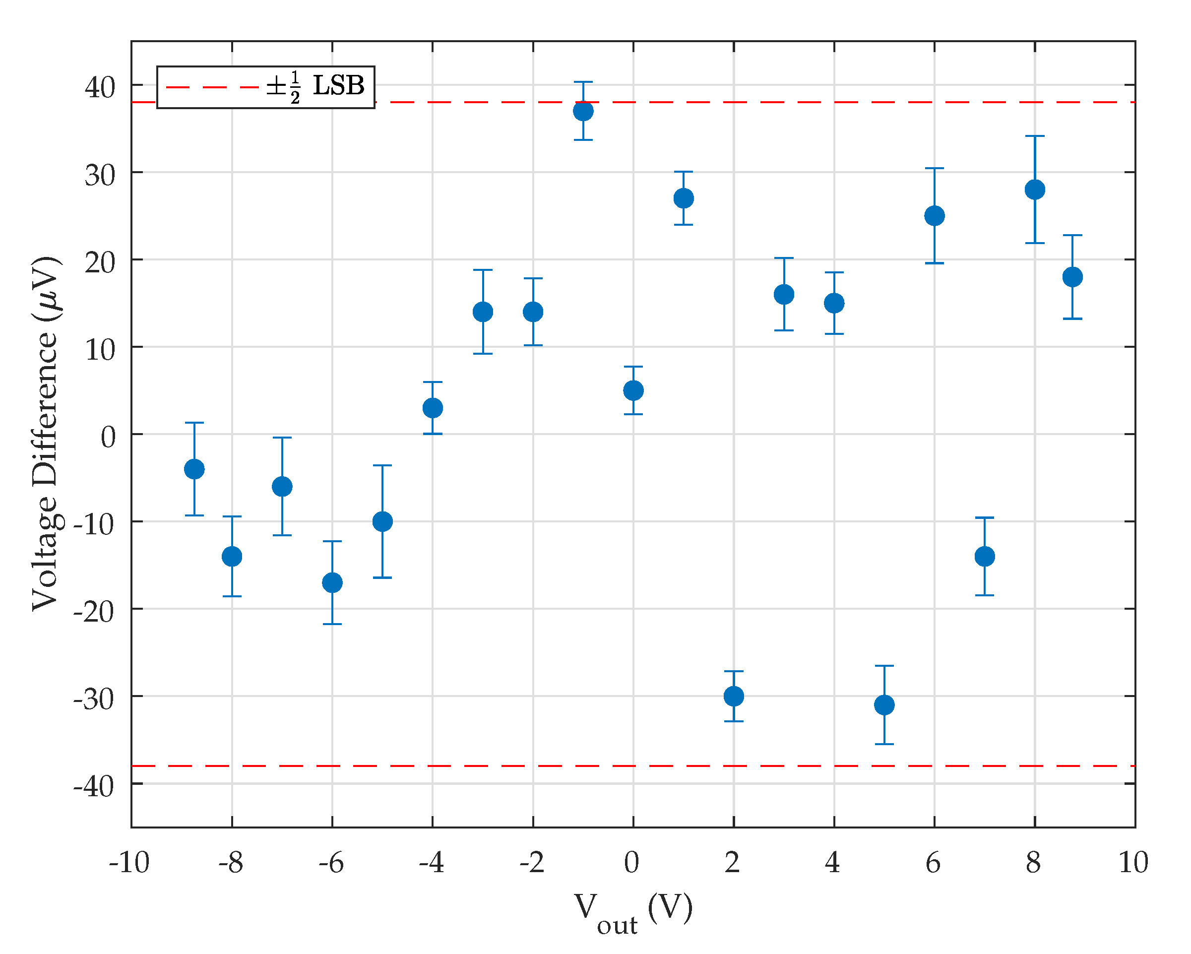
are plotted in Figure 16. It can be seen that all measurements lie within the expected range of ± M M 1 / 2 LSB from V out , with the error bars representing the standard deviation over 1000 consecutive repetitions. On RMS average, the repeatability thus evaluated is about 3 μ V or, equivalently, 0.04 LSB. The improvement compared to the voltage noise level can be attributed to the numerical integration suppressing high-frequency noise components. The RMS average of the mean errors across the whole input range is 141 μ V , corresponding to about 2 LSB. This is consistent with the residual error of V out reported in Section 5.1.

5.3. Integrator Drift

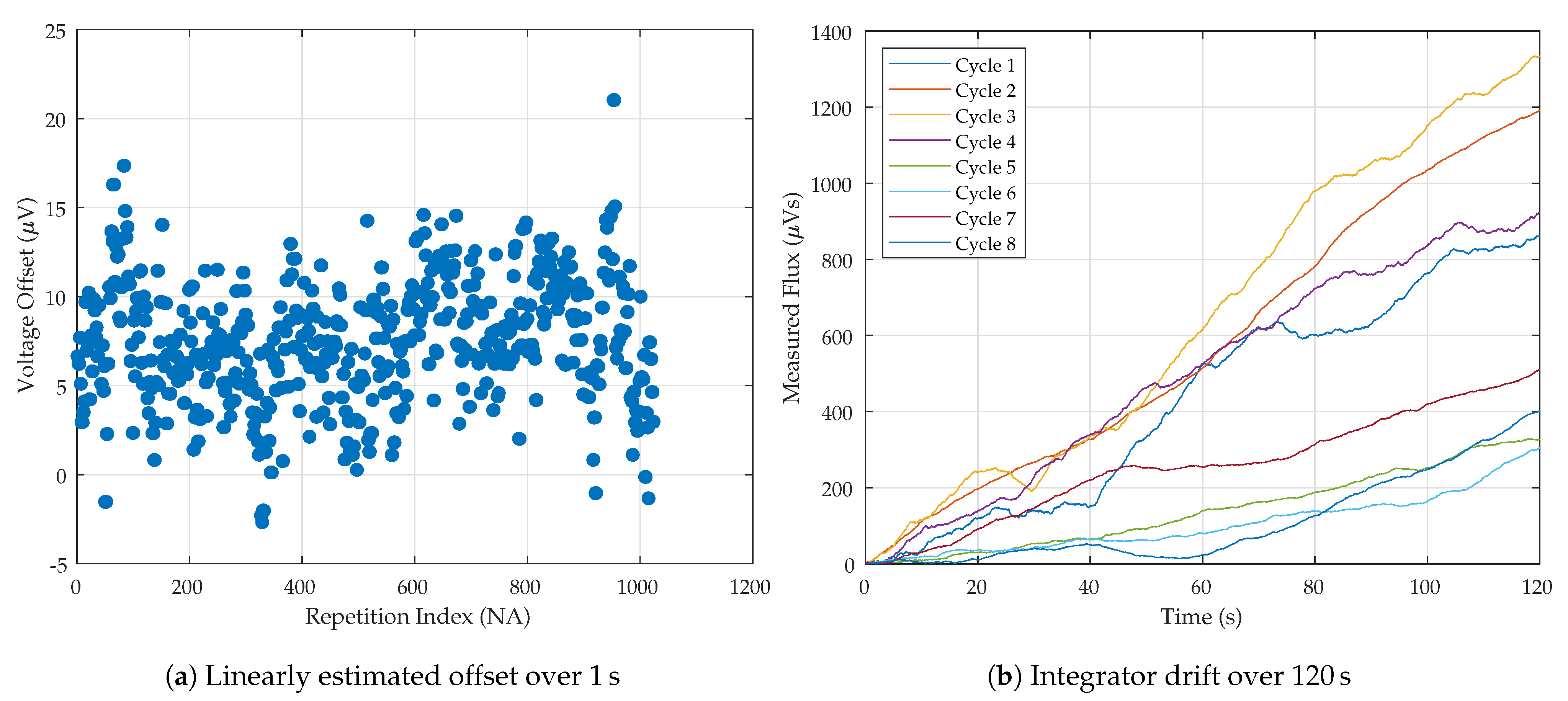
The short- and long-term performances of the in-built offset voltage compensation method have been evaluated by first shorting the input, then retrieving the measured flux waveforms over integration periods of duration Δ t = 1 s and Δ t = 120   s . The shortest duration is representative of the typical cycle lengths in most of CERN accelerators; at the other extreme, two minutes is the longest expected in ELENA antiproton cycles. Measurements were repeated, respectively, 1000 and 8 times, and the results are plotted in Figure 17a,b. The average and standard deviation of the equivalent voltage offset δ V = Δ Φ / Δ t are given in Table 2 for each set of measurements. The overall RMS voltage offset after the in-built correction is about 8 μ V , which under typical operating conditions, i.e., using a coil of area A c 1 m , is equivalent to a measured field drift of the order of 8 μ T / s . Such an error is usually acceptable for the shorter cycles but may not be so for longer ones; to cover for this case, a specific novel correction strategy is currently under development [40]. To conclude, we remark that the curves in Figure 17b illustrate the time evolution of the offset, which is observed to fluctuate with a scatter as large as 50 % of its mean value on a time scale of a few seconds.

6. Dynamic Performance

The amplitude transfer function and the latency of the whole acquisition chain were measured on a the test setup represented schematically in Figure 18, including: a signal generator, a complete FEC with Integrator, Simulated Field and WR output modules, an external WR switch (simulating the distribution network) and a WR receiver (simulating an end user). In the following subsection, the two tests are described in detail.

6.1. AC Amplitude Transfer Function

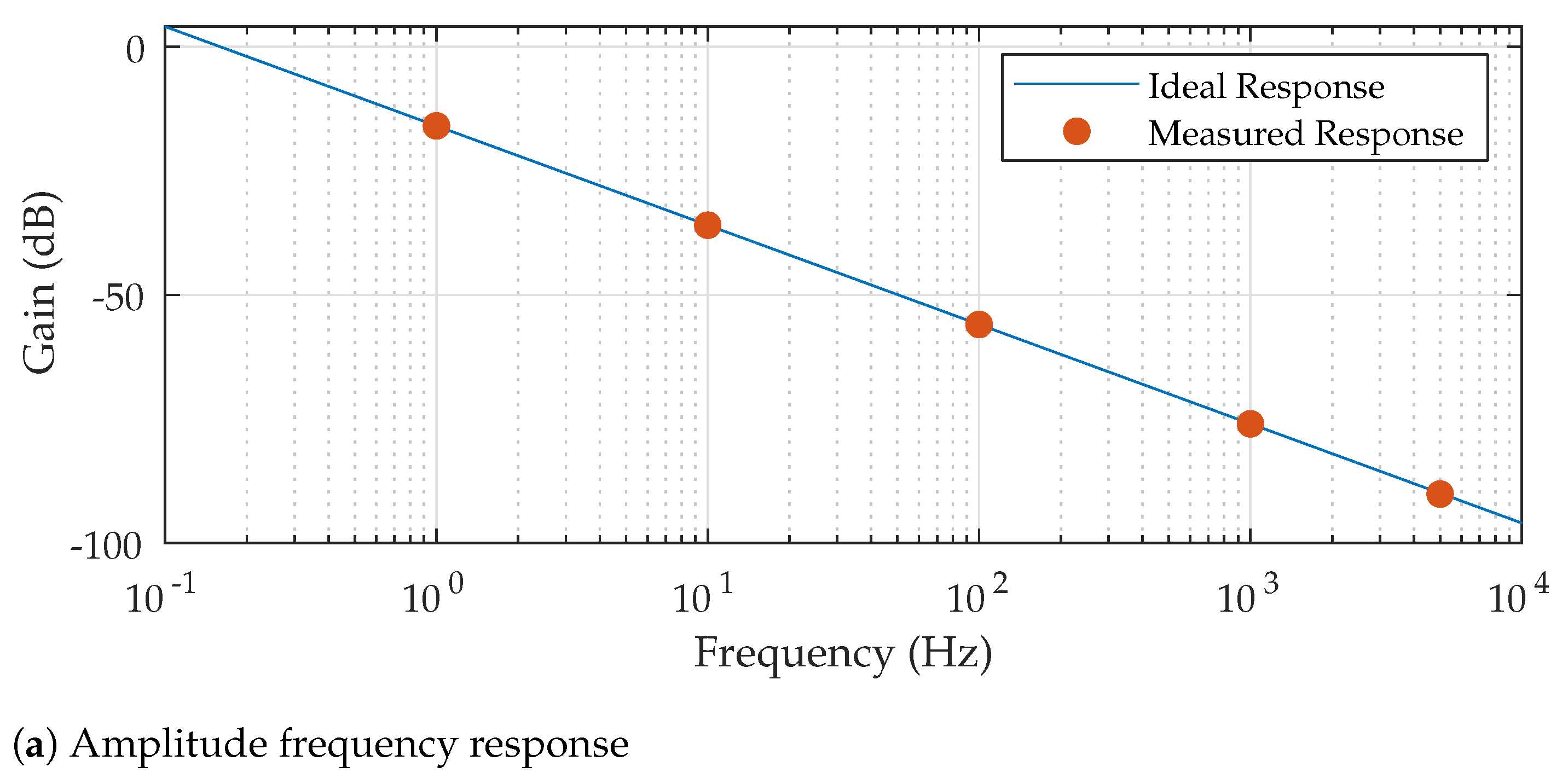
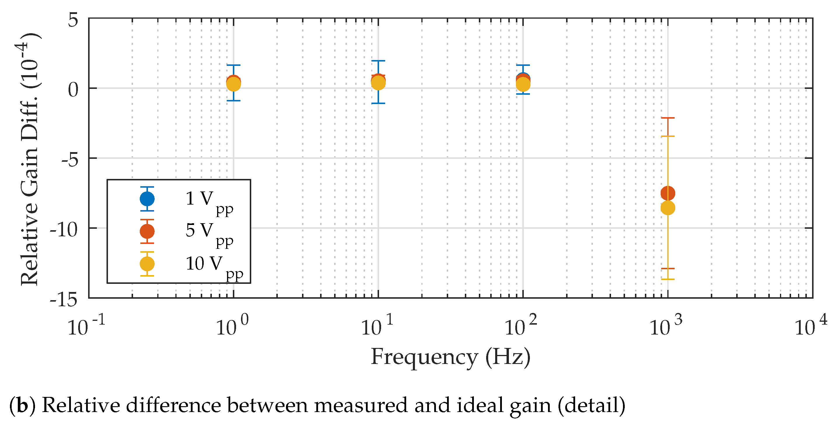
The gain response was measured as a function of frequency by injecting into the integrator for 1 s sine waves of varying amplitudes, i.e., 1, 5 and 10 V pp, and then retrieving the Δ Φ ( t ) waveform from the White Rabbit stream at the receiver’s end. For this test, the receiver used was a diagnostic system called a “WR Sniffer” [51], which is able to continuously stream multiple WR channels to disk at a peak aggregated rate of about 100 kfps. This entails an uncertainty of ± 10 μ s on any individual timing measurement, which can, however, be improved by averaging over a sufficiently high number of repetitions. The peak-to-peak amplitude of the response was then derived as the mean difference between successive maxima and minima, thereby cancelling out the effect of integrator drift. The amplitude response ratio is shown in Figure 19a along with the 20 dB/decade slope of an ideal integrator, while the difference between the two is magnified in Figure 19b. Below 100 Hz , mean errors are within the target tolerance of 100 ppm; whereas, starting from 1 k Hz , the effect of the anti-aliasing filters starts to manifest, and the error increases by several hundred ppm. For frequencies below 100 Hz , the scatter of the results, about 200 ppm , is comparable to the errors measured during the DC tests. At 1 k Hz , the scatter is about one order of magnitude higher, which could be ascribed to the decreasing number of samples per period.

6.2. Latency Measurements

The latency of the whole measurement chain is of fundamental importance for the qualification of the system as a feedback source for the user control loops and, in particular, for the RF subsystem. We analysed the propagation of a step change in the input along the chain, thus determining the contribution of each processing and transmission stage. The schematic layout of the test setup is shown in Figure 20.
A constant voltage was applied to the integrator input to generate a constant-slope ramp in the measured field . The initial time reference was given by the C0 cycle start trigger provided by a Central Timing Card, via the B-train crate. (All triggers and DIO connections are done via the crate, which does not appear in the layout for the sake of simplicity). The C0 trigger was used in place of a field marker to reset the integration to zero, thus providing an easy-to-identify falling edge propagating through the chain.
At the end of the chain, we set up a WR receiver, which for this test, consisted of an additional SPEC/FMC module, specifically designed for diagnostics. A single WR switch was included to reproduce the configuration common to most deployed systems.
To measure the propagation delay between components, we used two different, complementary methods: (1) the time interval between TTL triggers and/or the diagnostic analogue output of the modules was measured with a NI 6366 USB DAQ, sampling at 10 MSamples /s; (2) the timing information built in the WR stream was retrieved by means of the standard WR diagnostic facilities.
The tests were done at two different WR frame rates, i.e., 250 kfps , which is currently the default, and 100 kfps , which is under consideration to match the control loop requirements of the RF subsystem in the AD, ELENA, LEIR and PSB accelerators. The output data rate of the integrator remained fixed at 250 kfps in both cases.
The results obtained are summarized in Figure 20 and listed in detail in Table 3, Table 4 and Table 5, where we report their extrema, mean and standard deviation (jitter) over 10,000 repetitions.
We list below the different quantities that were measured and discuss the details of the procedure:
  • The overall mean propagation delay, 19.5 ± 2.3 μ s ( 2 σ ) at 250 kfps , was obtained from the time difference between C0 and a TTL trigger pulse emitted by the WR receiver as soon as it detected the field step change. The full statistics are reported in Table 3. This result is the most important, as it qualifies the whole acquisition chain. The accuracy of a single measurement is dominated by the frame period length in the WR stream, but due to the high number of repetitions, the uncertainty of the mean is as low as 0.02   μ s .
  • The WR delay from transmitter to receiver was measured as the time difference between C0 and a second TTL trigger pulse emitted by the WR receiver. For this, we injected C0 directly in the WR module via one of the two DIO connections available. There, the WR core set to 1 the start cycle flag in the header of the frames transmitted throughout the duration of the pulse. At the other end, the WR receiver generated a pulse upon arrival of the first active flag. The average delay thus measured is 7.3 ± 1.2 μ s @ 250 kfps (Table 3). The setup included a total fibre length of about 5 m , which adds a negligible delay, taking into account a typical propagation speed of 5 μ s / k m .
  • The WR delay was also cross-checked by subtracting the high-resolution, GPS- synchronized timestamps injected in every frame by the WR transmitter from the timestamp available at the receiver end. Again, the specific frame used was the first one to have its field marker flag set in the Frame Control header, thereby representing the rising edge of the field marker trigger pulse. The result obtained with this method is 3.9 ± 1.2 μ s @ 250 kfps (Table 4), which is significantly lower than the previous result. This difference can be ascribed to the functional sequence of the operations executed in the modules since timestamping is the last one before transmission and the first one upon reception. The uncertainty of each single timestamp difference is equal to the WR frame period, i.e., 4 μ s .
  • The delay due to the WR switch alone, i.e., 2.4 ± 0.1 μ s @ 250 kfps , was measured by repeating the previous test while bypassing the switch.
  • The details of the propagation through the FEC were measured by a different method based on generating an analog output image of the integrated field via the DAC built in the FMCs of the Integrator, the Simulated Field and the WR modules. (Since the Simulated Field module is by far the least computationally intensive of the three, its latency is very low, and the relative results were unstable, which is the reason why they are not reported here). The mean delays in the Integrator alone and in the whole chain up to the WR module are 4.4 and 10.9 μ s , respectively, with a single-take uncertainty of 1 μ s due to the sampling rate of the DAC.

Discussion

The overall delay is well below the specified tolerance of 30 μ s , even taking into account the possibility of multiple switches in the WR network, and of physical fibre lengths up to 100 m as it applies to most installations. (In the SPS, the B-train measurement is transmitted about 3 k m away to the beam dump subsystem, where it is used by the safety interlock PLC. As this subsystem has a high tolerance of about 1 m T , it is unaffected by the additional 15 μ s delay, even during fast field ramps).
When decreasing the WR frame rate to 100 kfps , the overall latency increases by about 3 μ s , which is half of what could have been expected from the 6 μ s frame period increase. However, this is consistent with the frame period itself being only a small component of the delay, which is dominated by the processing taking place in the three FEC modules in series.

7. Summary and Outlook

In this paper, we introduced the concepts behind the new FIRESTORM B-train systems at CERN, beginning with their role in a synchrotron, their method of operation, as well as the different sensors required for their implementation. The design of the systems was discussed, describing in detail the functions linked to magnetic flux integration, self-calibration and distribution over a White Rabbit network. We characterized experimentally the DC response of the system first, showing that after calibration, the voltage acquisition error across the ± 10 V input range has an arithmetic and an RMS mean of, respectively, 3 and 135 μ V (Section 5.1). We then integrated the same, known constant voltage inputs over one second and evaluated the equivalent voltage offset error, obtaining closely comparable results, thus proving the soundness of the integration stage (Section 5.2). Next, we carried out integration tests with the input shorted for up to 120 s , measuring an RMS average of an equivalent voltage offset of 8 μ V . Under typical operational conditions, these errors lead to a measurement drift of the order of 8 μ T s . Such offset, while remaining high in absolute terms, is much lower than in our legacy systems and is well within the tolerance of all magnetic cycles being run at this time.
We then proceeded to characterize the response of the system to time-changing inputs. First, we evaluated the measurement gain as a function of frequency for sine-wave inputs of varying amplitudes, showing that errors remain below the specified 100 ppm tolerance up to the required 100 bandwidth. Then, we quantified the contribution of all system components to the measurement latency, finding that overall, it remains always well below the specified 30 μ s tolerance. Therefore, we conclude that the new CERN B-train electronic acquisition system meets all its requirements, as it was also independently verified by running an extensive series of operational tests, as reported in detail in [7].
Nevertheless, certain improvements still seem necessary to guarantee compliance with upcoming, more challenging use cases. First of all, we are currently working on the algorithm to set optimally the fine offset correction Δ V 2 in (7), including the possibility of increasing the bit depth of the final flux integration stage so as to make the injection of an analogue voltage unnecessary (this would probably require newer, more capable FPGAs). An upgrade to the timing system is being considered to improve the internal LVDS transmission between SPEC modules in the FEC, which is currently a major limitation. For this, we need mechanisms to reduce the clock variation from board to board, either through adjustable oscillators or with the introduction of a master clock to synchronize the timing across all sub-systems. Finally, we look forward to implementing and testing different mathematical models in the prototype Predicted Field module during the upcoming operational run of the CERN complex.

Author Contributions

Conceptualization, D.G., A.B. and M.B.; methodology, J.V.W. and M.B.; software, D.G., V.D.C. and M.A.; validation, A.B., D.G., J.V.W., C.G., V.D.C. and M.A.; formal analysis, A.B., J.V.W., C.G., V.D.C. and M.A.; resources, D.G.; data curation, J.V.W. and V.D.C.; writing–original draft, J.V.W., M.B., A.B. and N.S.; writing–review and editing, J.V.W. and M.B.; supervision, M.B. and N.S.; project administration, M.B. and N.S. All authors have read and agreed to the published version of the manuscript.

Funding

This research received no external funding.

Acknowledgments

The authors would like to thank former and present CERN colleagues R. Avramidou, M. Colciago, D. Oberson and M. Roda for their essential contributions to the development and testing of the FIRESTORM B-train system, as well as M. Lipinski for developing the White Rabbit network, incorporating it into our system and carrying out tests.

Conflicts of Interest

The authors declare no conflict of interest.

References

  1. Bryant, P.; Johnsen, K. The Principles of Circular Accelerators and Storage Rings; Cambridge University Press: Cambridge, UK, 2005. [Google Scholar]
  2. Buzio, M.; Galbraith, P.; Gilardoni, S.; Giloteaux, D.; Golluccio, G.; Petrone, C.; Walckiers, L. Development of Upgraded Magnetic Instrumentation for CERN’s Real-time Reference Field Measurement Systems. In Proceedings of the 1st International Particle Accelerator Conference (IPAC’10), Kyoto, Japan, 23–28 May 2010; JACoW: Geneva, Switzerland, 2010; pp. 310–312. [Google Scholar]
  3. Franzini, G.; Coiro, O.; Pellegrini, D.; Serio, M.; Stella, A.; Pezzetta, M.; Pullia, M. Final Design and Features of the B-train System of CNAO. In Proceedings of the 1st International Particle Accelerator Conference (IPAC’10), Kyoto, Japan, 23–28 May 2010; JACoW: Geneva, Switzerland, 2010; pp. 2878–2880. [Google Scholar]
  4. Fraboulet, P.; Ambrosch, K.; Cesaris, I.D.; Beuret, A. The Current and Field Regulation System of the MedAustron Ion-Beam Accelerator. In Proceedings of the 39th Annual Conference of the IEEE Industrial Electronics Society (IECON 2013), Vienna, Austria, 10–13 November 2013; pp. 7103–7108. [Google Scholar] [CrossRef]
  5. Feldmeier, E.; Haberer, T.; Pters, A.; Schoemers, C.; Steiner, R. Magnetic Field Correction in Normal Conducting Synchrotrons. In Proceedings of the 1st International Particle Accelerator Conference (IPAC’10), Kyoto, Japan, 23–28 May 2010; JACoW: Geneva, Switzerland, 2010; pp. 675–677. [Google Scholar]
  6. Hanke, K.; Coupard, J.; Damerau, H.; Funken, A.; Goddard, B.; Lombardi, A.; Manglunki, D.; Mataguez, S.; Meddahi, M.; Mikulec, B.; et al. The LHC Injectors Upgrade (LIU) Project at CERN: Proton Injector Chain. In Proceedings of the 8th International Particle Accelerator Conference (IPAC’17), Copenhagen, Denmark, 14–19 May 2017; JACoW: Geneva, Switzerland, 2017; pp. 3335–3338. [Google Scholar] [CrossRef]
  7. Grech, C.; Amodeo, M.; Beaumont, A.; Buzio, M.; Di Capua, V.; Giloteaux, D.; Sammut, N.; Vella Wallbank, J. Error characterization and calibration of real-time magnetic field measurement systems. Nucl. Instrum. Methods Phys. Res. Sect. A Accel. Spectrom. Detect. Assoc. Equip. 2021, 990, 164979. [Google Scholar] [CrossRef]
  8. Burnet, J.P.; Giovannozzi, M.; Métral, E.; Michels, O.; Steerenberg, R.; Vandorpe, B. CERN Proton Synchrotron working point control using an improved version of the pole-face-windings and figure-of-eight loop powering. In Proceedings of the 10th European Particle Accelerator Conference (EPAC 2006), Edinburgh, UK, 26–30 June 2006; JACoW: Geneva, Switzerland, 2006; pp. 264–266. [Google Scholar]
  9. Benedikt, M.; Caspers, F.; Lindroos, M. Application of magnetic markers for precise measurement of magnetic fields in ramped accelerators. Part. Accel. 1999, 63, 57–73. [Google Scholar]
  10. Buzio, M. Fabrication and calibration of search coils. In Proceedings of the 2009 CAS-CERN Accelerator School: Specialised Course on Magnets, Bruges, Belgium, 16–25 June 2009; CERN: Geneva, Switzerland, 2009; pp. 387–421. [Google Scholar]
  11. Seo, S.H.; Werner, A.; Marquardt, M. Development of a digital integrator for the KSTAR device. Rev. Sci. Instrum. 2010, 81, 123507. [Google Scholar] [CrossRef] [PubMed]
  12. Feldmeier, E.; Haberer, T. Development of a High Precision Integrator for Analog Signals to Measure Magnetic Fields in Real-time. In Proceedings of the 4th International Particle Accelerator Conference (IPAC’13), Shanghai, China, 12–17 May 2013; JACoW: Geneva, Switzerland, 2013; pp. 661–663. [Google Scholar]
  13. Walckiers, L. Magnetic measurement with coils and wires. In Proceedings of the 2009 CAS-CERN Accelerator School: Specialised Course on Magnets, Bruges, Belgium, 16–25 June 2009; CERN: Geneva, Switzerland, 2009; pp. 357–385. [Google Scholar] [CrossRef]
  14. Grech, C.; Buzio, M.; Sammut, N. A Magnetic Measurement Model for Real-Time Control of Synchrotrons. IEEE Trans. Instrum. Meas. 2019, 69, 393–400. [Google Scholar] [CrossRef] [Green Version]
  15. Hancock, S. A Fit-Based Frequency Programme for the PS; Technical Report CERN-AB-Note-2007-036; CERN: Geneva, Switzerland, 2007. [Google Scholar]
  16. Pezzetta, M.; Bazzano, G.; Bressi, E.; Falbo, L.; Pullia, M.; Priano, C.; Coiro, O.; Franzini, G.; Pellegrini, D.; Serio, M.; et al. B-train Performances at CNAO. In Proceedings of the 2nd International Particle Accelerator Conference (IPAC’11), San Sebastian, Spain, 4–9 September 2011; JACoW: Geneva, Switzerland, 2011; pp. 568–570. [Google Scholar]
  17. Beaumont, A. NMR Magnetic Field Markers of the B-Train for the Proton Synchrotron Accelerator. Master’s Thesis, UTBM, Belfort, France, 2009. [Google Scholar]
  18. Benedikt, M.; Caspers, F.; Salvermoser, T. Absolute Calibration of the CERN PS-Booster Bending Field with Beam and NMR; Techreport PS-OP-Note-98-23; CERN: Geneva, Switzerland, 1998. [Google Scholar]
  19. Di Cesare, P.; Reymond, C.; Rottstock, H.; Sommer, P. SPS Magnetic Field Cycle Measurement System: Investigation on Nuclear Magnetic Resonnance (NMR) System to Get a Faster Reading of Field Values; Techreport CERN-SPS-PCO-Note 89-9; CERN: Geneva, Switzerland, 1989. [Google Scholar]
  20. Beaumont, A.; Buzio, M.; Boero, G. Ferrimagnetic Resonance Field Sensors for Particle Accelerators. Rev. Sci. Instrum. 2019, 90, 065005. [Google Scholar] [CrossRef] [PubMed]
  21. METROLAB. PT2025 NMR Teslameter User Manual, 2nd ed.; METROLAB Instruments SA: Geneva, Switzerland, 2003. [Google Scholar]
  22. Grech, C.; Beaumont, A.; Buzio, M.; Sammut, N. Performance comparison of Nuclear Magnetic Resonance and FerriMagnetic Resonance field markers for the control of low-energy Synchrotrons. J. Phys. Conf. Ser. 2018, 1065, 052022. [Google Scholar] [CrossRef]
  23. AimTTi. Aim-TTi TF930, 8th ed.; AIM & Thandar Thurlby Instruments: Cambridgeshire, UK; Available online: https://resources.aimtti.com/manuals/TF930_Instruction_Manual-English-Iss8.pdf (accessed on 8 July 2020).
  24. Gilardoni, S.; Manglunki, D.E. Fifty Years of the CERN Proton Synchrotron: Volume 1; Techreport CERN-2011-004; CERN: Geneva, Switzerland, 2011. [Google Scholar]
  25. Beaumont, A.; Giloteaux, D.; Matheoud, A.V.; Buzio, M.; Boero, G. Electron paramagnetic resonance magnetic field sensors for particle accelerators. Rev. Sci. Instrum. 2020, 91, 105001. [Google Scholar] [CrossRef] [PubMed]
  26. Open Hardware Repository. Available online: https://ohwr.org/ (accessed on 8 July 2020).
  27. Loschmidt, P.; Gaderer, G.; Simanic, N.; Hussain, A.; Moreira, P. White rabbit—Sensor/actuator protocol for the CERN LHC particle accelerator. In Proceedings of the 8th Annual IEEE Conference on Sensors (IEEE Sensors 2009), Christchurch, New Zealand, 25–28 October 2009; pp. 781–786. [Google Scholar] [CrossRef]
  28. Jansweijer, P.; Peek, H.; de Wolf, E. White Rabbit: Sub-nanosecond timing over Ethernet. Nucl. Instrum. Methods Phys. Res. A 2013, 725, 187–190. [Google Scholar] [CrossRef]
  29. Siemens. SIMATIC IPC847E, 1st ed.; A5E43920357-AA; Siemens AG: Nurnberg, Germany, 2018. [Google Scholar]
  30. About CentOS. Available online: https://centos.org/about/ (accessed on 8 July 2020).
  31. Arruat, M.; Fernandez, L.; Jackson, S.; Locci, F.; Nougaret, J.L.; Peryt, M.; Radeva, A.; Sobczak, M.; Vanden Eynden, M. Front-End Software Architecture. In Proceedings of the 11th International Conference on Accelerator and Large Experimental Physics Control Systems (ICALEPCS07), Knoxville, TN, USA, 15–19 October 2007; JACoW: Geneva, Switzerland, 2007; pp. 310–312. [Google Scholar]
  32. Alvarez-Sanchez, P.; Bau, J.C.; Domínguez, D.; Lewis, J.; Serrano, J. The Evolution of the CERN SPS Timing System for the LHC Era. In Proceedings of the 9th International Conference on Accelerator and Large Experimental Physics Control Systems (ICALEPCS2003), Gyeongju, Korea, 13–17 October 2003; JACoW: Geneva, Switzerland, 2003; pp. 125–127. [Google Scholar]
  33. Simple PCIe FMC Carrier (SPEC). Available online: https://www.ohwr.org/project/spec/wikis/home (accessed on 8 July 2020).
  34. Xilinx. Spartan 6 FPGA. Xilinx. 2011. Available online: https://www.xilinx.com/support/documentation/data_sheets/ds160.pdf (accessed on 8 July 2020).
  35. WISHBONE. Revision B.4 Specification, OpenCores. Available online: https://cdn.opencores.org/downloads/wbspec_b4.pdf (accessed on 8 July 2020).
  36. Wishbone Slave Generator. Wishbone Tool Developed by OHWR. Available online: https://ohwr.org/project/wishbone-gen/ (accessed on 8 July 2020).
  37. VITA. FPGA Mezzanine Card (FMC) Standard; Approved in 2008, Revised in 2010; VMEbus Internationa Trade Association: Fountain Hills, AZ, USA, 2008. [Google Scholar]
  38. Bojtar, L. OASIS User Manual. 2009. Available online: https://cds.cern.ch/record/1164782 (accessed on 8 July 2020).
  39. Alvarez, P. CTR User Guide; Technical Report; CERN: Geneva, Switzerland, 2007. [Google Scholar]
  40. Amodeo, M.; Arpaia, P.; Buzio, M. Integrator Drift Compensation of Magnetic Flux Transducers by Feed-Forward Correction. Sensors 2019, 19, 5455. [Google Scholar] [CrossRef] [Green Version]
  41. Arpaia, P.; Bottura, L.; Fiscarelli, L.; Walckiers, L. Performance of a fast digital integrator in on-field magnetic measurements for particle accelerators. Rev. Sci. Instrum. 2012, 83, 024702. [Google Scholar] [CrossRef] [PubMed] [Green Version]
  42. Keysight. Agilent Technologies 34401A Digital Multimeter Manual, 10th ed.; Keysight Technologies: Santa Rosa, CA, USA, 2014; Available online: https://www.keysight.com/zz/en/assets/9018-01063/user-manuals/9018-01063.pdf (accessed on 8 July 2020).
  43. Jacquet, D.; Gorbonosov, R.; Kruk, G. LSA—The High Level Application Software of the LHC—And Its Performance During the First Three Years of Operation. In Proceedings of the 14th International Conference on Accelerator and Large Experimental Physics Control Systems (ICALEPCS 2013), San Francisco, CA, USA, 6–11 October 2013; JACoW: Geneva, Switzerland, 2013; pp. 1201–1204. [Google Scholar]
  44. Argyropoulos, T.; Bohl, T.; Lasheen, A.; Papotti, G.; Quartullo, D.; Shaposhnikova, E. Momentum slip-stacking in CERN SPS for the ion beams. In Proceedings of the 10th International Particle Accelerator Conference (IPAC’19), Melbourne, Australia, 19–24 May 2019; JACoW: Geneva, Switzerland, 2019; pp. 3184–3187. [Google Scholar] [CrossRef]
  45. Todesco, E.; Aquilina, N.; Auchmann, B.; Bottura, L.; Buzio, M.; Chritin, R.; Deferne, G.; Deniau, L.; Fiscarelli, L.; Hagen, P.; et al. The Magnetic Model of the LHC in the Early Phase of Beam Commissioning; Technical Report CERN-ATS-2010-154; CERN: Geneva, Switzerland, 2010. [Google Scholar]
  46. Caspers, F.; Heinze, W.; Lewis, J.; Lindroos, M.; Salvermoser, T. An Alternative to Classical Real-time Magnetic Field Measurements using a Magnet Model. In Proceedings of the 6th International Conference on Accelerator and Large Experimental Physics Control Systems (ICALEPCS’97), Beijing, China, 3–7 November 1997; CERN: Geneva, Switzerland, 1997; pp. 581–584. [Google Scholar]
  47. Grech, C.; Buzio, M.; Pentella, M.; Sammut, N. Dynamic Ferromagnetic Hysteresis Modelling Using a Preisach-Recurrent Neural Network Model. Materials 2020, 13, 2561. [Google Scholar] [CrossRef]
  48. Perrelet, D.; Brischetto, Y.; Damerau, H.; Oberson, D.; Sundal, M.; Villanueva, A. White-Rabbit Based Revolution Frequency Program for the Longitudinal Beam Control of the CERN PS. In Proceedings of the 15th International Conference on Accelerator and Large Experimental Physics Control Systems (ICALEPCS 2015), Melbourne, Australia, 17–23 October 2015; JACoW: Geneva, Switzerland, 2015; pp. 286–290. [Google Scholar] [CrossRef]
  49. Lipinski, M.M. BTrain-over-WhiteRabbit Wiki. Available online: https://gitlab.cern.ch/BTrain-TEAM/Btrain-over-WhiteRabbit/wikis/home (accessed on 8 July 2020).
  50. Analogic. Data Precision 8200 User Manual. Available online: https://testequipment.center/Product_Documents/Data-Precision-8200-Specifications-0E813.pdf (accessed on 8 July 2020).
  51. Arpaia, P.; Di Capua, V.; Roda, M.; Buzio, M. Real-Time Magnetic Measurement Monitoring under cRIO-LabVIEW Based Platform; EasyChair Preprint No. 1335; EasyChair: Manchester, UK, 2019. [Google Scholar]
Figure 1. (a) The ELENA ring B-train reference magnet, equipped with an integral, curved induction coil and an NMR probe placed at the center of the magnet’s gap (shown in the inset). The magnetic field inside the gap is vertical and uniform to a very good approximation. (b) Schematic representation of CERN’s ELENA synchrotron ring.
Electronics 10 02140 g001
Figure 2. Schematic example of a sequence of magnetic cycles in the Proton Synchrotron.
Electronics 10 02140 g002
Figure 3. Functional scheme of the field measurement.
Electronics 10 02140 g003
Figure 4. Field marker block diagram.
Electronics 10 02140 g004
Figure 5. Block diagram of the main functions composing the FIRESTORM system.
Electronics 10 02140 g005
Figure 6. The architecture of the FEC, depicting the software hierarchy as well the flow of data through the FEC.
Electronics 10 02140 g006
Figure 7. SPEC Card with EDA-03557 FMC card installed.
Electronics 10 02140 g007
Figure 8. The front side of the B-train crate, showing the various 3U Eurocard front panels associated with the FMC modules.
Electronics 10 02140 g008
Figure 9. Field marker trigger generator FMC.
Electronics 10 02140 g009
Figure 10. Integrator module FMC.
Electronics 10 02140 g010
Figure 11. Schematic flowchart of the integrator, including offset and gain correction. The green blocks denote analogue processing steps, while the yellow ones represent processing in the digital domain.
Electronics 10 02140 g011
Figure 12. Schematic representation of the Simulated Field dataflow.
Electronics 10 02140 g012
Figure 13. EDA-03557 front view mounted on a SPEC card.
Electronics 10 02140 g013
Figure 14. A functional diagram of the broadcast White Rabbit Ethernet frame.
Electronics 10 02140 g014
Figure 15. The difference of FIRESTORM digital voltages with respect to the measured input value.
Electronics 10 02140 g015
Figure 16. The mean and standard deviation of Δ V e (13) over the full input dynamic range.
Electronics 10 02140 g016
Figure 17. The results of integrator drift tests.
Electronics 10 02140 g017
Figure 18. Schematic layout of the dynamic performance test setup.
Electronics 10 02140 g018
Figure 19. AC gain response results.
Electronics 10 02140 g019aElectronics 10 02140 g019b
Figure 20. Latency test of the different components of the acquisition and transmission chain @ 250 kfps. In red, TTL trigger pulses associated with the cycle start C0; in green, the analogue outputs of the SPEC modules; and in cyan, quantities derived from the WR frame. The horizontal axis is used to represent time differences (not to scale).
Electronics 10 02140 g020
Table 1. A comparison between calibration methods.
Calibration Method Δ V 1 ( μ V) G cc 1 (ppm)
In-built Correction381221
Manual Linear Least-Squares Fit423220
Table 2. The linearly estimated offset voltage.
Integration Period (s)Mean ( μ V) σ ( μ V)
17.73.5
1206.53.6
Table 3. The overall FIRESTORM latency at different transmission speeds.
Input to Output
at 250 kHz ( μ s)
Transmission
at 250 kHz ( μ s)
Input to Output
at 100 kHz ( μ s)
Transmission
at 100 kHz ( μ s)
Average19.57.322.68.3
Minimum15.64.915.75.0
Maximum23.89.929.711.7
σ 2.31.23.61.9
Table 4. Delay across the White Rabbit network @ 250 kfps.
Without Switch ( μ s)With Switch ( μ s)
Average1.533.93
Minimum1.523.86
Maximum4.327.2
σ 0.130.13
Table 5. Internal FEC propagation time @ 250 kfps.
C 0 to Integrator DAC ( μ s) C 0 to WR DAC ( μ s)
Average4.410.9
Minimum1.88.4
Maximum6.813.3
σ 1.21.7
Publisher’s Note: MDPI stays neutral with regard to jurisdictional claims in published maps and institutional affiliations.