Article

A Method for Selection of Power MOSFETs to Minimize Power Dissipation

1
Queensland Micro- and Nanotechnology Centre, Griffith University, Brisbane, QLD 4111, Australia
2
Department of Electronics & Communication Engineering, Graphic Era (Deemed to Be University), Dehradun 248002, Uttarakhand, India
*
Author to whom correspondence should be addressed.
Electronics 2021, 10(17), 2150; https://doi.org/10.3390/electronics10172150
Submission received: 26 July 2021 / Revised: 30 August 2021 / Accepted: 31 August 2021 / Published: 3 September 2021
(This article belongs to the Section Power Electronics)

Abstract

:
A balance between static and dynamic losses of a power MOSFET is always desirable for accomplishing the maximum efficiency for a specific power converter. The standard semiconductor theory suggests that a minimum power dissipation in a MOSFET can be achieved by selecting a specific device active area. However, for power circuit designers, the active device area is unknown given that only datasheet parameters are available. Hence, in this paper, we propose a simple method, based on semiconductor theory, to select optimum power MOSFET from a family of MOSFETs using only datasheet parameters. By applying this optimization method to the specific power supply circuit under development, power engineers can select the best transistors to yield lowest power losses for the systems under development.

1. Introduction

Power semiconductor devices form the core of the modern power conversion systems. The overall efficiency of the power converters depends mainly on the losses attributed to power semiconductor devices. Therefore, a thorough understanding and selection of the power semiconductor device are required for designing efficient and reliable power converters.
One such popular and widely used power semiconductor device is a power MOSFET. The total power dissipation in a power MOSFET consists of static loss that is determined by the on-resistance and dynamic loss that is determined by the parasitic capacitances [1]. The standard semiconductor theory shows that the total power dissipation has a minimum for specific device active area [2]. This happens because an increase in the active area reduces the on-resistance, reducing static loss, but it increases the parasitic capacitances, increasing the dynamic loss. However, the active device area that minimizes the total power dissipation depends on specific circuit configuration and parameters, such as the on-state current flowing through the power MOSFET and the switching frequency. Because of that, the device manufacturers cannot provide a single optimum MOSFET for all applications and instead offer a family of MOSFETs manufactured by the same process but with different on-resistances [3]. On the other hand, the power circuit designers do not know the active device area and the other needed semiconductor device parameters to determine the minimum power dissipation for a particular application; hence, they cannot use the standard semiconductor theory of active device area to select the MOSFET with the optimum on-resistance.
In this paper, we propose a method for this selection, which is based on semiconductor theory, using only datasheet parameters such as on-resistance and energy related effective output capacitance. The proposed method is demonstrated by commercial superjunction (SJ) MOSFETs and silicon carbide (SiC) MOSFETs.

2. Proposed Method

The maximum current handling capability of any power MOSFET is generally limited by the on-resistance (RON). The total RON of a power MOSFET structure comprises many individual resistances connected in series between the drain and the source terminal. However, the contribution of the channel resistance (RCH), the accumulation resistance (RA), the JFET resistance (RJFET), and the drift region resistance (Rdrift) is significantly higher than the rest of the resistances, therefore dominating the value of static losses [2]. It must be noted that all the contributing resistances are inversely proportional to the channel width (W) [2,4].
The switching characteristics of a power MOSFET are mainly determined by its intrinsic parasitic capacitances. The parasitic capacitances of the power MOSFET can be classified as input capacitance (CISS) and output capacitance (COSS). At higher voltages and switching frequencies, the dynamic losses due to charging/discharging of COSS dominate the switching performance [5]. Hence, in this brief, the dynamic power dissipation by COSS is given more consideration than the influence of CISS. COSS comprises gate-to-drain (CGD) and drain-to-source (CDS) capacitance. Both CGD and CDS span the depletion region, which is directly proportional to W; hence, COSS as a function of W can be expressed as [6,7]:
C O S S = L W q ε N D 2 V
where q is the charge of an electron, ε is the semiconductor permittivity, ND is the donor doping density, and V is the applied drain-to-source voltage.
Because the power MOSFET datasheets do not show the device parameter W, the power circuit designers cannot use it to calculate the resistances and the capacitances and, therefore, cannot use the corresponding equations to select the power MOSFET that will minimize the power losses. On the other hand, RON and COSS are available on every datasheet. From the standard semiconductor theory, it is clear that RON is inversely proportional to W and COSS is directly proportional to W. This means that:
R O N C O S S = κ
where κ is a constant that groups all technological parameters for the specific family of MOSFETs. The constant κ is effectively a figure of merit for a family of MOSFETs. In fact, if we integrate COSS curve with respect to V and replace COSS with the integrated charge, QOSS, we obtain a well-known figure of merit: RON · QOSS [8]. However, most manufacturers do not provide QOSSV curves in the datasheets. Instead, most datasheets provide energy-related effective output capacitance, Co(er). The reason for introducing Co(er) is the nonlinear nature of COSS, which makes it difficult for a circuit designer to analyze power circuits. The constant capacitance Co(er) is defined as the capacitance that gives the same stored energy as COSS while V is rising from 0 to 80% of the drain-to-source breakdown voltage, and it is given by [9]:
C o ( e r ) = 2 V 2 0 V C O S S ( v ) × v d v
Because the value of Co(er) is available in most datasheets, it is convenient to use it in (2) instead of the voltage-dependent COSS:
R O N C o ( e r ) = κ
The dynamic power dissipation due to charging/discharging of Co(er) is given by [2,10,11]:
P d y n a m i c = f C o ( e r ) V 2
where f is the switching frequency. Using (4) and (5) can be expressed in terms of RON as:
P d y n a m i c = ( f κ V 2 ) / R O N
The static power dissipation can be expressed by the standard equation [1,2,11]:
P s t a t i c = D R O N I 2
where D is the duty cycle and I is the root-mean-square drain current. Combining (6) and (7), we can express the total power dissipation in terms of RON as the parameter distinguishing different MOSFETs from the same family:
P t o t a l = D R O N I 2 + ( f κ V 2 ) / R O N
To minimize the total power losses with respect to RON, the derivative of (8) is set to zero and the optimum RON is derived as:
d P t o t a l d R O N = 0     R O N ( f ) = V I f κ D
Equation (9) shows that Ptotal has a minimum for a specific RON, depending on the values of V, f, D, and I. In the next section, the proposed method for selection of the optimum RON is demonstrated with SJ MOSFETs.

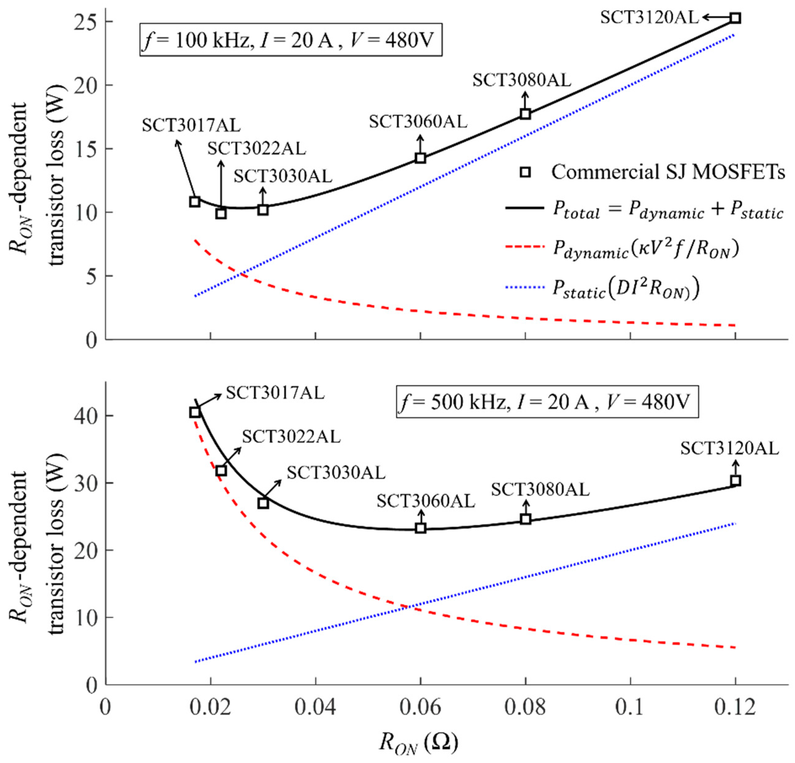
3. Demonstration of the Proposed Method Using SJ MOSFETS

Superjunction devices consist of multiple, alternate highly doped n and p semiconductor stripes leading to lower RON without sacrificing the blocking voltage. Hence, for the same breakdown voltage, the RON of SJ MOSFETs will be much lower than the conventional Si-based planar MOSFETs.
To demonstrate the proposed method described in the previous section, nine Infineon 650 V CoolMOS C3 technology SJ MOSFETs were considered. Individual κ values were calculated using (4) by taking RON and Co(er) values from the respective SJ MOSFET datasheets. The mean of all the individual κ values was equal to 1.835 × 10⁻¹¹ ΩF, and this value was taken to represent this family of MOSFETs. The values of Co(er) in the datasheets were given for V = 480 V, and this voltage was used in (6). Since the SJ MOSFETs have different current ratings, the current of the lowest rated SJ MOSFET current, I = 2.5 A, was utilized.
Using D = 0.5, κ = 1.835 × 10⁻¹¹ ΩF, V = 480 V, and I = 2.5 A, the theoretical static, dynamic, and total losses were calculated and are shown in Figure 1. For the same bias voltage, current, and duty cycle, the total losses for individual SJ MOSFETs were calculated using their respective κ in (8) and are also shown in Figure 1. Despite the variation of individual κ values around the mean value of 1.835 × 10⁻¹¹ ΩF, the total losses of the commercial SJ MOSFETs follow the trend of the proposed theory, as can be seen from Figure 1. For f = 20 kHz and f = 100 kHz, the minimum losses are occurring for RON = 164.5 mΩ and RON = 367.8 mΩ, respectively. For the power converter operating at V = 480 V, I = 2.5 A, and f = 20 kHz, SJ MOSFETs SPW47N60C3, SPW35N60C3, SPW24N60C3, and SPW20N60C3 are the best selection because they minimize the power loss. However, the selection of the best MOSFET changes for higher frequencies. The maximum switching frequency of 100 kHz was used for this demonstration because CISS of CoolMOS C3 family of MOSFETs is quite large, and higher switching frequencies are practically not feasible. For the power converter operating at the same bias voltage and current but at the switching frequency of 100 kHz, SJ MOSFET SPP11N60C3 provides the minimum power loss. It can be observed from Figure 1 that the optimal RON increases as the switching frequency increases. This is because the switching losses due to the parasitic capacitances begin to dominate at higher switching frequencies. To minimize the dominant switching losses, a MOSFET with a smaller capacitance has to be selected, and this MOSFET will have a smaller channel width (Equation (1)), which in turn means that RON of this MOSFET is larger.
For a different family of MOSFETs, corresponding to a different technology process, the constant κ has a different value. At Infineon, the CoolMOS CE family of MOSFETs is based on newer and better optimized technology. The CISS of CoolMOS CE family of MOSFETs is lower than that of the CoolMOS C3 family of MOSFETs, enabling them to operable at higher switching frequencies. Hence, in order to show the effectiveness of the proposed method, nine 600 V SJ MOSFETs from the CoolMOS CE family were considered. For CoolMOS CE family, the mean κ = 1.453 × 10⁻¹¹ ΩF was used to calculate the theoretical static, dynamic, and total losses, as shown in Figure 2. The voltage, current, and duty cycle were kept the same. For f = 100 kHz and f = 500 kHz, the minimum losses are occurring at RON = 327.3 mΩ and RON = 731.9 mΩ, respectively. Hence, for the power converter operating at 100 kHz, SJ MOSFET IPAW60R280CE should be selected to minimize the power loss, whereas IPAW60R460CE is the best choice when the power converter operates at 500 kHz.
For the case of a higher output current, static losses starts to dominate the dynamic losses. By keeping switching frequency at 100 kHz, the proposed theory was applied to CoolMOS CE family of MOSFETs for higher currents, as shown in Figure 3. It can be seen from Figure 3 that the SJ MOSFET with the lowest RON, i.e., IPAW60R190CE, is the best for power converters operating at output currents higher than 5 A.

4. Validation

A widely used clamped inductive load circuit was used in LTSPICE to validate the proposed approach. The circuit parameters for the simulation were: VDD = 480 V, IDD = 2.5 A, RG = 25 Ω, VGG = 15 V, f = 100 kHz, D = 0.5, tr = 30 ns, tf = 20 ns, LS = LD = LG = 5 pH, and a 650 V SiC Schottky diode (SCS320AJ). The CoolMOS C3 family MOSFET models provided by the Infineon were utilized in the configured circuit. These models include the parasitic inductances and capacitances of the power MOSFET. Apart from COSS, the dynamic losses of a power MOSFET are mainly influenced by the transistor switching time and diode reverse recovery. The diode reverse recovery loss is a fraction of transistor switching time loss and hence is neglected in the paper. The transistor switching time loss is attributed to CISS of the MOSFET, and the power loss due to this switching time can be calculated as [11]:
P s w t = V × I × f × ( Q G S + Q G D ) I G
where IG is the gate current and (QGS + QGD)/IG determines the rate of charging/discharging CISS by the gate driver. The term (QGS + QGD)/IG is inversely proportional to RON for a family of MOSFETs. Hence, for lower RON, higher charge is required, and for higher RON, lower charge is required to charge CISS of the MOSFET. Charging and discharging of CISS is through the channel of the MOSFET, and hence for each MOSFET of the same family, the actual VDS waveform depends on RON of the corresponding MOSFET. In the Miller region, the inductive load fixes the drain current at a constant value ID, which means that VDS can be replaced by RON × ID. Therefore, the switching time in (10) becomes independent of RON. The consequence of this observation is that the minimum power dissipation appears at the same RON, regardless of the actual value of IG and the RON-independent power dissipation due to IG. The constant for the theory was estimated to be 3 W by comparing (6) to the LTSPICE simulation of the already found optimized MOSFET in CoolMOS C3 family, i.e., SPP11N60C3. Hence, the entire theoretical total loss curve for f = 100 kHz as shown in Figure 1 was raised by 3 W and was compared with the LTSPICE simulation of each MOSFET, as shown in Figure 4.
It is quite clear from the simulation results shown in Figure 4 that the switching time and the parasitic inductances of the MOSFET do not impact the selection of the MOSFET and follow a similar trend. Still, the optimized MOSFET to choose from the CoolMOS C3 family for the given circuit conditions is SPP11N60C3. The theory quite matches all the available simulated MOSFETs, which shows the effectiveness of the proposed approach.

5. Application of the Proposed Method to SiC MOSFETs

Wide band gap devices such as SiC MOSFETs have emerged as a potential alternative to conventional Si-based power devices for numerous power converter applications. To demonstrate the proposed method, six commercially available 650 V SiC MOSFETs from ROHM Semiconductor were used. The mean value of κ for this family of MOSFETs was 5.775 × 10⁻¹² ΩF. The comparison of the transistor loss obtained from (8) and the power losses of individual SiC MOSFETs, at constant output current of 20 A, is shown in Figure 5. As expected, the power loss is minimized by a MOSFET with a higher on-state resistance when the switching frequency is increased. In the specific case of 100 kHz, the MOSFET SCT3022AL minimizes the power loss, whereas the SCT3060AL should be selected for the switching frequency of 500 kHz.

6. Conclusions

A method to select optimum power MOSFET from a family of MOSFETs considering only datasheet parameters, such as RON and Co(er), is proposed in this paper. The proposed method is demonstrated with two families of Infineon SJ MOSFETs, CoolMOS C3 and CoolMOS CE. The proposed method is validated in LTSPICE using CoolMOS C3 models provided by the manufacturer. The proposed method is further demonstrated with the SiC MOSFETs family from ROHM Semiconductor. The validation of the proposed method with LTSPICE shows that the average values of current and voltage are sufficient for the purpose of selecting the MOSFET with optimum RON. The simulation with LTSPICE produced typical current and voltage waveforms. That is why the agreement between the power dissipation obtained by LTSPICE simulation (with the typical waveforms) and the power dissipation obtained with the proposed analytical equation (using the average values of current and voltage) demonstrates that the average values are sufficient for this purpose. By applying this optimization method to the specific power supply circuit under development, power engineers can select the commercial power MOSFET with the specific RON that maximizes the power efficiency of the designed circuit.

Author Contributions

Conceptualization, U.J. and S.D.; methodology, U.J., S.D. and F.M.-Y.; software, U.J.; validation, U.J., S.D., F.M.-Y., H.A.M., P.P. and M.C.; formal analysis, U.J. and S.D.; investigation, U.J., S.D., F.M.-Y., H.A.M. and M.C.; resources, S.D. and F.M.-Y.; data curation, U.J.; writing—original draft preparation, U.J. and S.D.; writing—review and editing, U.J., S.D., F.M.-Y., H.A.M., P.P. and M.C.; visualization, U.J. and S.D.; supervision, S.D., F.M.-Y. and H.A.M.; project administration, S.D.; funding acquisition, S.D. and F.M.-Y. All authors have read and agreed to the published version of the manuscript.

Funding

This research was funded by Innovative Manufacturing Cooperative Research Centre (IMCRC), and BlueGlass as the industry partner, grant number 220132.

Data Availability Statement

Data is contained within the article.

Acknowledgments

The authors would like to acknowledge Innovative Manufacturing Cooperative Research Centre (IMCRC) for providing scholarship to the first author. We also acknowledge School of Engineering and Built Environments (EBE) of Griffith University for funding this project. This work was performed in part at the Queensland node of the Australian National Fabrication Facility, a company established under the National Collaborative Research Infrastructure Strategy to provide nano- and micro-fabrication facilities for Australia’s researchers.

Conflicts of Interest

The authors declare no conflict of interest.

References

  1. Erickson, R.W. Switch Realization. Fundamentals of Power Electronics; Chapman & Hall: New York, NY, USA, 1997; pp. 49–104. [Google Scholar]
  2. Baliga, B.J. Fundamentals of Power Semiconductor Devices, 2nd ed.; Springer: Raleigh, NA, USA, 2019; pp. 413–449. [Google Scholar]
  3. Christian, M.; Olivier, G. Optimum MOSFET Selection for Synchronous Rectification. Infineon Application Note. Available online: https://www.infineon.com/dgdl/Infineon˗MOSFET_OptiMOS_optimum_selection_for_synchronous_rectification˗AN˗v01_00˗EN.pdf?fileId=db3a30431ff988150120664202606c8b (accessed on 26 January 2021).
  4. Dimitrijev, S. Principles of Semiconductor Devices, 2nd ed.; Oxford University Press: New York, NY, USA, 2012; pp. 312–316. [Google Scholar]
  5. Costinett, D.; Maksimovic, D.; Zane, R. Circuit-Oriented Treatment of Nonlinear Capacitances in Switched-Mode Power Supplies. IEEE Trans. Power Electron. 2015, 30, 985–995. [Google Scholar] [CrossRef]
  6. Nakajima, A.; Shimizu, M.; Ohashi, H. Power Loss Limit in Unipolar Switching Devices: Comparison Between Si Superjunction Devices and Wide-Bandgap Devices. IEEE Trans. Electron. Devices. 2009, 56, 2652–2656. [Google Scholar] [CrossRef]
  7. Sze, S.M. Semiconductor Devices: Physics and Technology; Wiley: New York, NY, USA, 1985; p. 84. [Google Scholar]
  8. Hopkins, A.; McNeill, N.; Anthony, P.; Mellor, P. Figure of merit for selecting super-junction MOSFETs in high efficiency voltage source converters. In Proceedings of the 2015 IEEE Energy Conversion Congress and Exposition (ECCE), Montreal, QC, Canada, 20–24 September 2015; pp. 3788–3793. [Google Scholar] [CrossRef] [Green Version]
  9. Toshiba Power MOSFET Electrical Characteristics Application Note. Available online: https://toshiba.semicon-storage.com/info/docget.jsp?did=13415 (accessed on 26 January 2021).
  10. Xiong, Y.; Sun, S.; Jia, H.; Shea, P.; Shen, Z.J. New physical insights on power MOSFET switching losses. IEEE Trans. Power Electron. 2009, 24, 525–531. [Google Scholar] [CrossRef]
  11. Lakkas, G. MOSFET Power Losses and How They Affect Power Supply Efficiency. Analog Application Journal. Available online: http://www.ti.com/lit/an/slyt664/slyt664.pdf (accessed on 26 January 2021).
Figure 1. Comparison of the proposed theory at a constant output current of 2.5 A with the commercially available Infineon CoolMOS C3 technology SJ MOSFETs.
Electronics 10 02150 g001
Figure 2. Comparison of the proposed theory at constant output current of 2.5 A with the commercially available Infineon CoolMOS CE technology SJ MOSFETs.
Electronics 10 02150 g002
Figure 3. Comparison of the proposed theory at constant switching frequency of 100 kHz with the commercially available Infineon CoolMOS CE technology SJ MOSFETs.
Electronics 10 02150 g003
Figure 4. Comparison of the proposed theory with LTSPICE simulation on clamped inductive load circuit.
Electronics 10 02150 g004
Figure 5. Comparison of the proposed theory at constant output current of 20 A with the commercial ROHM SiC MOSFETs.
Electronics 10 02150 g005
Publisher’s Note: MDPI stays neutral with regard to jurisdictional claims in published maps and institutional affiliations.

