Article

Space Imaging Sensor Power Supply Filtering: Improving EMC Margin Assessment with Clustering and Sensitivity Analyses

by
Laurent Patier
1,2 and
Sébastien Lalléchère
3,4,*
1
Detection Chain Team, CNES, 31000 Toulouse, France
2
Electro-Magnetic Compatibility (EMC) Society, IEEE, 75000 Paris, France
3
AFSCET, Systemic Scientific Society, 75000 Paris, France
4
Institut Pascal, Université Clermont Auvergne, 63000 Clermont-Ferrand, France
*
Author to whom correspondence should be addressed.
Electronics 2021, 10(18), 2301; https://doi.org/10.3390/electronics10182301
Submission received: 17 August 2021 / Revised: 12 September 2021 / Accepted: 14 September 2021 / Published: 18 September 2021
(This article belongs to the Special Issue Electromagnetic Interference and Compatibility, Volume II)

Abstract

:
This work is dedicated to the assessment of the filtering performances of an optoelectronic sensor for space applications. Particular care is taken concerning the power supply subsystem (here voltage shifter integrated circuit), which is part of the electromagnetic compatibility (EMC) compliance of an imaging equipment embedded on spacecrafts. The proposed methodology aims at two major targets: First, evaluating the Filter Effectiveness (FE) subject concerning varying parameters (including filter topology, parasitic effects and source/load impedance variations); second, quantifying the relative importance of representative equivalent electrical components through sensitivity analyses (nominal and parasitic values). The latter point is of utmost importance considering the expected versatility of such systems, such as manufacturing tolerances, for instance. Nominal values and/or components are often badly defined for confidentiality reasons, lack of knowledge or pure ignorance of inputs. An analytical deterministic formulation (here through the transfer matrix approach) is proposed and completed with an original stochastic strategy (Reduced Order Clustering, ROC). This ensures the reliable assessment of both statistical filter performances and most influential parameters, jointly with computational resources saving relatively to brute force Monte Carlo simulations.

1. Introduction

1.1. Space Mission Needs

An important field of space applications is devoted to Earth observation. Wavelength is not especially focused on the visible range (from 350 to 750 nm) because of the measurement of chemical pieces, such as O 2 , CO 2 or H 2 O, supposed to detect peaks of resonance at infrared (IR) bands ( λ I R > 750 nm). For these electro-optical performances, we could mention InGaAs (In x Ga 1 x As: Indium gallium arsenide, with variable bandgap energy, from 0.4 to 1.4 eV, depending on proportion of x) and HgCdTe (Hg x Cd 1 x Te: Mercury cadmium telluride, with variable bandgap energy, from 0 to 1.5 eV, depending on proportion of x) materials, which compose the substrate of the detection layer for optoelectronic sensors, with the huge attribute of an adjustable wavelength responsivity [1].
However, a big challenge is to maximize the signal because of very weak amplitude, mainly due to the weak flux (blackbody spectrum) and also the low energy of IR photons. To have a sufficient signal to noise and distortion ratio (SINAD; SINAD results from a combination of Signal to Noise Ratio (SNR) and Total Harmonic Distorsion (THD)), the detection instrument should be a very sensitive sensor (with very low analog voltages, less than typical 1 mV = 60 dB μ V) and immunity should be achieved to limit the susceptibility levels (improvement of Shielding and Filtering Effectiveness, respectively, SE and FE).
Concerning the video chain electronics, CMOS Read-Out Integrated Circuits (ROIC) have a low noise of around 1 e only (with CVF (CVF = Charge to Voltage Factor) typically around 100 μ V / e ): The sensitivity is now around 0.1 mV (40 dB μ V). Therefore, the immunity analysis is a foreground aspect. In this context, the imaging sensor is the core of the detection chain (see Figure 1) and the challenge is focused on the cohabitation of the different natures of signals:
  • analog voltage, stems from electro-optical conversion; then Low Noise (pre-)Amplification (LNA) stage;
  • power supply of output stage of LNA;
  • digital signals, as clocks (for cadence pixels, lines and frames), as numerical voltage after Analog/Digital Conversion (ADC).
In order to reduce the noise (and so improve the SNR) coupled on the video signal (see the green path, with analog stages, links, PCB and/or flex: Output stage, pre-amplification, until programmable gain amplifier, just before analog-to-digital conversion),a particular focus is provided concerning the Power Supply Rejection Ratio (PSRR), with a specific analysis of the FE of the sensor power mains.

1.2. Diversity of Electronic Components and Electromagnetic Systems

From an EMC point of view, it is admitted that both the power systems’ emission and their efficiency at the filter stage, just like Shielding Effectiveness (SE), play major roles. In this framework, the influence of systems’ variability has been documented for a long time, dealing with a large diversity of Uncertainty Quantification (UQ) and measurements.
In this paper, the authors are focusing on two distinct classes of uncertainty:
  • The quantification of measurements: Parallel to metrological needs, the state-of-the-art fully treated the uncertainty;
  • the intrinsic nature of varying inputs: The lack of knowledge (pure ignorance or confidential applications) of parameters, here due to the physical parameters themselves, or their environment for instance.
The first kind of UQ may be depicted in the precious work reported in [2]. It deals with the uncertainty calculation of filter attenuation EMC measurements. This part is very well documented and the interested reader may refer to [3] to obtain a global overview for experimental EMC and electromagnetic interference (EMI) expectations in this framework. This study of the state-of-the-art is completed in [4] considering computational uncertainties, reviewing existing methods and alternatives to the gold standard Monte Carlo (MC) approach. Recent papers have demonstrated the interest of UQ and/or Uncertainty Propagation (UP) for a diversity of electronic and electromagnetic applications: Reliability and antenna modelling in [5], electronic design in [6] and power electronics in [7].
For the second kind of UQ, a representative example may be given from the distribution of radio-frequency (RF) impedances of power conductors, as achieved in North America and Europe in [8]. In this framework, a set of data was carefully collected and studied considering statistical dispersion (here through mean, minimum and maximum) of power lines RF impedance magnitudes. Similarly to previous cases, various studies were achieved at subsystem levels, e.g., common mode filter based on Electromagnetic Band Gap (EBG) structures in [9]. In this study, de Paulis et al. have pointed out the influence of manufacturing uncertainties through experimental validations for an 8 GHz EBG common filter. In this context, particular care should be taken with parasitic effects of components since it may lead to drastic aftermaths at a component level as pointed out in [10]. In this framework, the parasitic resistance, inductance and capacitance (respectively, ESR, ESL, EPR and EPC 5 ; in the same way that the parasitic effects of a capacitor may be expressed by Equivalent Series Resistance (ESR) and Inductance (ESL), we may use EPR and EPC for Equivalent Parallel Resistance and Capacitance of an inductor) could play major roles whether their initial values are badly known.
Thus, uncertain variations of ESR, ESL, EPR and EPC should be sharply taken into account when designing electronic systems and EMC filters in particular. While data sheets and tabulated power line filter Insertion Loss (IL) and/or attenuation are well documented, the use of power line filtering data remains a harsh task considering data mainly come from a 50 Ω test setup. The use of 50 Ω impedance datasets is continuously questioned in many books and technical papers, including measurement standards such as CISPR 17 [11] and/or MIL-STD-220 [12]. In this context, CISPR 17 proposes alternative techniques to IL 50 Ω testing: They target the assessment of the Filter Efficiency (FE) in real functioning uses rather than in artificial configurations.
The statement of the problem is rooted in real life situations where a power filter or filtering system is not matched with 50 Ω terminal impedances. Actually, and as previously pointed out when dealing with UQ, the filter termination is usually purely unknown (here both value highly varying with frequency and are badly known by nature due to the diversity of equipment and their use). Mostly EMC and electromagnetic standardization procedures (e.g., [11]) rely on worst case analysis to provide sufficient margin levels to avoid systems’ malfunctions due to EMIs.
In this framework, the current paper is organized as follows: Section 2 illustrates the importance of the filtering system considered in this work, including the definition of the equivalent electrical model, the nature of the uncertain parameters and the global methodology proposed to assess the effect of UQ modeling. The methods attached to UQ are described in Section 3: MC and Random Order Clustering (ROC) strategies. Then, Section 4 is devoted to the presentation and discussion of results obtained in two distinct test cases, including random assumptions around the electrical equivalent definition of the filter, with deterministic (Test case #1) or random (Test case #2) sources and loads. This section also provides an exhaustive study of the influence of each input through a sensitivity analysis (SA) of the problem. Finally, a summary of the capability of the proposed ROC method to handle the UQ issue is developed in the conclusion, Section 5.

2. Problem Statement

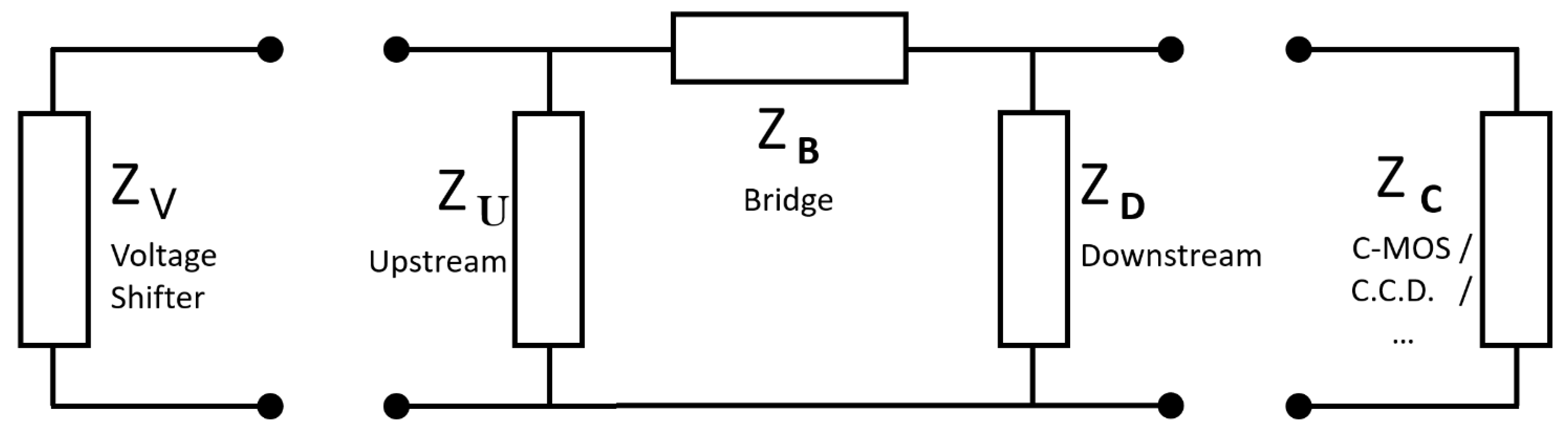
2.1. Analog Voltage Power Filter and Detection Instrument Electronic Architecture

On the one hand, power supplies are generally imposed in voltages by technologies, which should be varied for a rich electronics system like imaging sensor and its proximity electronics (see Figure 1, with Clock Drivers and Load Driver especially). For example, the Transistor–Transistor Logic (TTL) classically uses 5 V bus, while the Complementary Metal-Oxyde Semiconductor (CMOS) could use 3.3 V.
On the other hand, sensors like CCD need higher (and not standard) voltages, around 10 V, to increase the dynamic range, through the Full Well Capacity (FWC), which is a key parameter of image sensors. Moreover, this voltage should be adjusted to optimize the signal integrity.
It is not realistic to consider that each voltage needed by the sensor (see polar stage, Figure 1), should be directly wired from the Power Control and Distribution Unit (PCDU) of the spacecraft’s platform: The number, the weight and the cost of wires should be prohibitive; and from the EMC point of view, coupling through theses bundles should drastically impact the power supply cleanliness.
Moreover, depending on the choice of packaging for the imaging instrument and the associated constraints (See the blue dividing, with Micro-camera cube + Treatment unit, or else orange dividing, with Image sensor + Proximity electronics + Video chain board), a Secondary Power Supply is provided by a Step-Down Transformer (SDT), also called Step-Down Voltage Converter—as DC/DC or Point-of-Load (POL) regulator—to deliver standard voltages of the board: 3 V 3, 5 V, etc.
Then, even if it does not seem to be logical to use SDT then immediatly after use a Step-Up Transformer (SUT), it is yet done in practice, with a component called Voltage Shifter (also called “Level” Shifter) as shown Figure 2. From the electrical point of view, it is not really aberrant, because only very low power is consummed (<1 W): This explains why this choice of topology remains a good architecture for this type of instrument.

2.1.1. Voltage Shifter

In the function of the mission constraints (as thermal, EMC, etc.), the choice of the detection instrument architecture should vary. It concerns which electronic stage will be located on the proximity board—either the same chip of the photosensitive elements, not on another board in a separated housing like video electronics (see Figure 1, the functional link of video signals, from Detection Layer stage to the On-Board Computer, OBC). In the function of the subsystem housing, configurations may lead from many electronics linked by flex striplines and other bundles (Orange band segmentation: Image sensor + Proximity electronics + Video chain board), to “all integrated” 3D-stacked microcamera cube (Blue band segmentation: Micro camera “cube” + Treatment unit) [1].
Concerning the EMC aspects, this choice is not straightforward, mainly due to the difficulty of reaching high levels of SE for cables (especially for the first test case with microstrips and flex wiring). In the context of the all-integrated cube, the proximity effects have to be considered rigorously, especially when dealing with the EMC study of the parasitic capacitance.
In an imaging sensor, a big challenge is to integrate, around the same stage, the low level analog output signal (with high sloping clocks, to decrease non-linearity due to the jitter) and power tracks (where ripple due to other instruments is still noisy). Moreover, the crosstalk between pulse sequencer clocks and power supply voltages should be noticeable. Therefore, an excellent FE is required in the upstream part of the sensor.

2.1.2. L Filter–Pi Filter–Component Trade-off

The filtering of the (noisy) Voltage Shifter’s power supply towards (clean) sensor voltage should be achieved by a classical Π -architecture, illustrated in Figure 3.
The complex impedances are designated with initials like:
  • V for the Voltage shifter,
  • U for Upstream side component of Π -filter (capacitor),
  • B for Bridge component (inductor),
  • D for Downstream side component (capacitor),
  • and C for typical “CCD” or “CMOS” sensor.
Concerning the upstream impedance, we should consider two cases of architecture:
  • the case of L (or Γ ) structure ( Z U is, in this case omitted), which should be better if the voltage shifter is considered as very low impedance: It concerns the results of channels #1 and #4;
  • the case of Π structure (capacitor at Z U ), where the FE is increased by the decoupling capacitance (compared to the non-negligible impedance of the voltage shifter): Channels #2 and #3.
Concerning the bridge impedance, two similar inductors of 1 µH are compared: Firstly, with 3232 package (traditional reference from source of supply, considered at channels #1 and #3); secondly, with 1212 package (smaller package, with a priori less parasitic characteristics (EPR, EPC), at channels #2 and #4). We have to note that, for space instruments, the miniaturization is not the challenge, because of the hardness constraints against energetic particles (impacting the whole spacecraft).
Concerning the downstream impedance, four cases are compared:
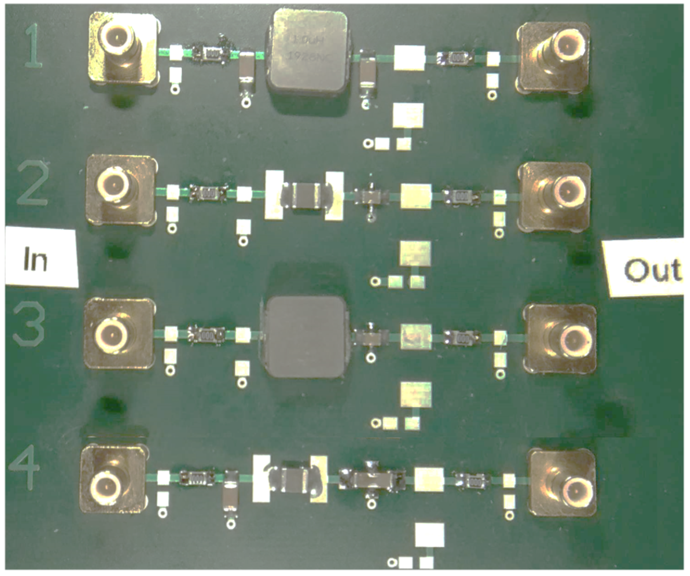
  • channel #1: A traditional capacitance of 4.7 µF (4.7 µF is the baseline value for an excellent FE, in first analysis), from type X7R in 1210 package.
  • channel #2: A very low ESL technology capacitor of 1.5 µF (1.5 µF is the maximum value of capacitance for this technology in 0805 package with 10 V of maximum voltage rating, which is a 0% derating consideration for 10 V polarization) in 0805 package.
  • channel #3: A very low ESL technology capacitor of 1.0 µF (1.0 µF is the maximum value of capacitance for this technology in 0805 package with 16 V of maximum voltage rating, which is 60% derating consideration for 10 V polarization) in 0805 package.
  • channel #4: A very low ESL technology capacitor of 4.7 µF in 1210 package.

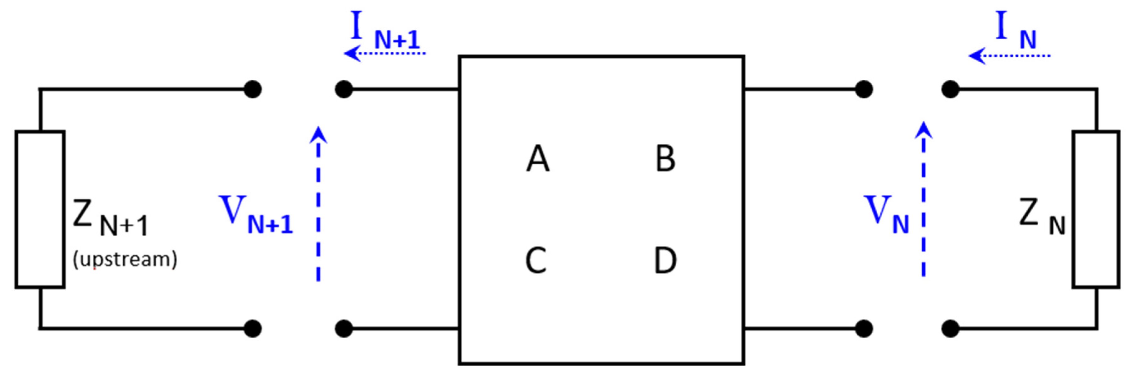
2.1.3. Electrical Models

For low impedances such as Z V (Voltage shifter), Z U (Upstream) and Z D (Downstream) the serial model of RLC (Figure 4a) will be used. For high impedances such as Z B (Bridge) and Z C (CCD) the parallel model of RLC (Figure 4b) will be used.
As we previously explained, the FE is improved when mismatch is raised; thus, it is legitimate to question the usefulness of the upstream capacitor when the voltage shifter is assumed as low impedance. Therefore, Figure 5 shows the four channels, where theses influences ( Γ and Π architectures, inductors with “big”/3232 or “small”/1212 packages and X7R and low ESL capacitor) are both implemented on board, in order to measure and simulate these effects.

2.2. Pi-Filter Robustness to Uncertain Working Conditions

2.2.1. Pi-Filter Modeling: Test Case #1

The UQ of inputs is always a hard task, both from industrial and academic points of view, since the parameters are often badly known or purely ignored, e.g., for suppliers’ confidentiality reasons or due to environmental conditions/manufacturing tolerances (see [9]). As a first test case, Table 1 and Table 2 summarize the 10 components needed for the pi-filter electrical equivalent model, respectively, for channels #1 and #4.

2.2.2. Variability at Source and Load Levels: Test Case #2

This test case includes four extra parameters with random assumptions, as listed in Table 3. It is well known that nominal measurements led with standard 50 Ω -source/ 50 Ω -load requirements may be subjected to huge variations when dealing with an embedded system and variable sources/loads. The purpose of test case #2 is to define the statistical assumptions due to power variations (voltage shifter integrated circuit) and realistic variations of source and load impedances.

2.3. Measurements with Vector Network Analyzer (VNA)

Classically, IL should be measured with a Vectorial Network Analyzer (VNA), considering the S 21 parameter, where input and output impedances (actually loading the filter) are equal to 50 Ω . Unlike the transfer function (which remains ambiguous for filter characterization), the FE (or the IL) have the advantage of quantifying the performance of a filter unambiguously, which is the ratio between transmission without filter ( S 21 1 0 dB), then with filter ( S 21 1/IL ≡ –IL d B ).
The measurements were performed with Rohde&Schwarz ZNL 3, with two 1 m-length RG58/KX15 cables. A “2 ports” calibration (Open, Short, Load) was applied before measurements (calibration stage). In total, 801 frequency points were acquired between 100 kHz and 1 GHz (log-spaced distribution), as illustrated in Figure 6.
Figure 6 gives an overview of the measured data, considered from four tracks of a test board (here depicted as channels #1 to #4, see Figure 7A).

2.4. Analytical Characterization with Chain Matrix Retro-Simulations

This section is devoted to the description of the analytical characterization of the filter behaviour with chain matrix retro-fitting.
The global methodology of the proposed work is summarized in Figure 7. It follows five main steps:
  • A/ Measurements on VNA of four channels on Test board (see measured results in Figure 6).
  • B/ Retro-fitting with chain matrix (semi-analytical) model optimization.
  • C/ Spice model validation: Deterministic simulation of pi-filter.
  • D/ Uncertainty Quantification, assuming random variations of electrical equivalent components.
  • E/ Filter margins assessments (statistical distribution) and Sensitivity Analysis (SA).
The aim of this measurement is to compare with simulations, to properly calibrate the analytical model.

2.4.1. Methodology

Now, IL should be estimated with retro-simulation, to fit with measurements at 50 Ω for each impedance: At source (voltage shifter) and at load stage (image sensor), as shown in the following with calculated statistical data and Spice-like deterministic simulation (Sim.).
After validating the analytical model (e.g., the results were both compared with Tensorial Analysis of Network (TAN) derived from works in [13], data not shown here, and Spice simulations with measurements.. The next level (Step D in Figure 7) aims at quantifying the filter performance through realistic impedance assumptions taking into account intrinsic drifts of electronics components and sources (see, respectively, test cases #1 and #2). The aim is, after validation of the model with measurements, to extrapolate the impedance conditions to a more realistic one, where it is complicated to do some developments and tests.

2.4.2. Analytical Model–Chain Matrix

When dealing with the FE calculation, the chain (or transfer) matrix technique appears as a powerful tool to assess IL levels. The voltage/current ( V , I ) state should be expressed as a couple; then the ( V N + 1 , I N + 1 ) couple at the upstream stage could be expressed as a function of the previous V/I state, ( V N , I N ) couple, at downstream.
Assuming [ T ] N as a 2 × 2 matrix (also called the ABCD matrix model), it is admitted the inner terms are given as follows:
T = [ A B C D ]
We voluntarily omit the subscript N of T-matrix, this in order to lighten the notation, leading to the implicit relationship, see Figure 8:
( V I ) N + 1 = [ A B C D ] N · ( V I ) N
In the case of the Π filter, if we consider Y U as the Upstream admittance, Z B as the Bridge impedance and Y D as the Downstream admittance, we could easily find the four ABCD terms, as follows:
A = 1 + Y D · Z B
B = Z B
C = Y U + Y D + Y U · Y D · Z B
D = 1 + Y U · Z B
Another advantage to using the chain matrix is we could easily have the Filter Effectiveness F E as a function in terms of ABCD [14]:
F E = A · Z C + B + C · Z V · Z C + D · Z V Z V + Z C
where Z V denotes the Voltage shifter output impedance (or “source” side of the filter) and Z C the Charge-Coupled Device input impedance (or “load”). All measurements and simulations are computed as S 21 = 1 / F E (or S 21 d B = F E d B while expressed in decibels). Furthermore, two test cases will be considered in the following with VNA impedances:
  • where Z V = Z C = 50   Ω (test case #1, see Table 1 and Table 2),
  • where Z V and Z C are subject to random variations (test case #2, Table 3).

2.4.3. Results

In the following, particular care will be given to the comparisons between measured data and simulated results, from an analytical model. Measurements and simulations (Figure 9) demonstrate that the Π -architecture filter (channels #1 and #4) offers better performances than the Γ -architecture filter (channels #2 and #3), for lower frequencies ( f 1 MHz) and also for higher frequencies (which is even more important for our applications of image sensors). This expresses that “low impedance” of voltage shifter is not justified compared to the upstream capacitor performances.
We have to notice that curves for channels #2 and #3 (Figure 9) are interrupted because of propagation phenomena, not taken into account in our model, and which have a non negligible effect around ≳30 MHz. Indeed, pixel clock frequencies classically work around more than 1 Msps: Logically, bands >1 MHz are the focus of the best immunity for these products, with the relative coupling I L tends to near 90 dB around f 0 10 MHz.
Relying on the deterministic analysis of the filtering module, the present work aims at assessing the impact of variations (e.g., due to manufacturing tolerances) on FE. The main objective is to select the filter characteristics fitting at best with the uncertain constraints.
The following section aims at briefly presenting the fundamental principles of stochastic methods developed in this work.

3. Stochastic Theoretical Foundations

3.1. Sampling Techniques: Monte Carlo and Reduced Order Clustering Methods

The stochastic part of this work is freely adapted from the techniques used in [15] to model composite materials with random locations of conductive inclusions. As depicted in Figure 7, Step D2, with two Random Variables (RVs), the random assumptions (Figure 7, Step D1) are modelled through the golden standard MC sampling (see, for instance, the work given in [16] to predict the scaling of the electromagnetic interference from large systems). In the following, the brute force MC method will be considered as a reference with high sampling rates (here with n MC = 100,000 simulations).
The foundations of the ROC technique rely on clustering principles, well known for their capability to handle complex problems with a limited number of random samples. The work proposed in this paper is based on classical k-mean techniques (for the interested reader, details may be found in [17]). The main steps of the ROC technique are summarized as follows:
  • Step 1: Setting n MC random points (here 100,000 MC simulations) for d RVs (in the following d 1 = 10 or d 2 = 14 RVs, respectively, for test case #1 or #2);
  • Step 2: Sampling n ROC randomly chosen points, targeting most representative points among n MC d-space random inputs;
  • Step 3: Computing d-component distance between n ROC samples to n MC initial set of MC inputs;
  • Step 4: Optimising n ROC samples aiming to keep most representative datasets (i.e., here, minimizing distance figure of merit in Step 3).
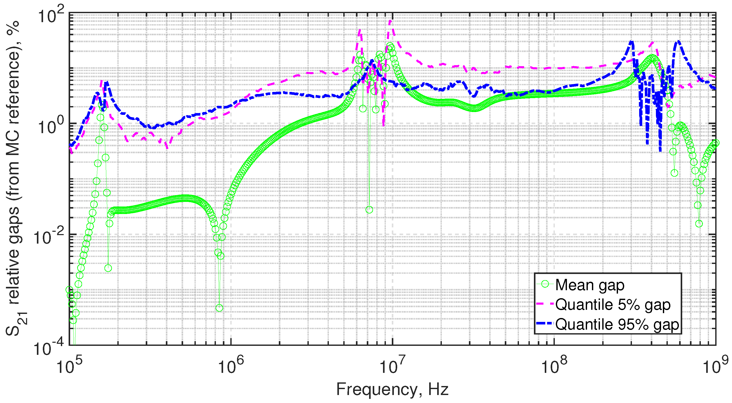
This work relies on an updated k-mean algorithm: The inputs are defined with the random vector X j ( j = 1 , , d 1 or d 2 number of RVs, respectively), for test cases #1 ( d 1 = 10 ) or #2 ( d 2 = 14 ). The ROC procedure provides the optimised dataset ( x ^ i , w i ) for i = 1 , , n ROC where x ^ i is the sample number from the initial n MC MC samples. Finally, the mean value of the chosen output (here, the S 21 parameter) is defined as follows:
S 21 ( f ) = i = 1 n ROC w i S 21 x ^ i ( f ) ,
where S 21 ( f ) is the averaged S 21 parameter at frequency f and S 21 x ^ i ( f ) stands for S 21 parameter extracted from MC sample number x ^ i . The variance of the S 21 parameter is given as follows:
v a r S 21 ( f ) = i = 1 n ROC w i S 21 x ^ i ( f ) S 21 ( f ) 2 .
Finally, the Cumulative Density Function (CDF) of S 21 parameter can be extracted by sorting, at each frequency f, the list of weighted pairs ( S 21 x ^ i ( f ) , w i ) .
Figure 10 gives an illustration of the ROC assessment of filter performances, through CDF reconstruction (staircasing data in pairs ( S 21 x ^ i ( f ) , w i ) , i = 1 , , n ROC ) for low and high frequencies (respectively, f L = 400 kHz on left side and f H = 800 MHz on right side), given α and 1 α quantile levels (here α = 10%). In the following, particular care will be given to higher quantile levels ( α = 5 %) to characterize the quality of the ROC design of experiments with respect to MC reference results.
Figure 10 shows the results agree well between ROC and MC data at frequencies f L and f H . Despite the good agreement between ROC and MC simulations, it is worth pointing out that the quality of results depends on:
  • The needed quantile level ( α ). Of course, extreme quantiles (i.e., lowering α -levels) will require an increasing number of simulations, both for ROC and MC methods. Thus, we will consider in the following the relative gaps (in percents) existing between ROC filter statistics (e.g., considering mean, standard deviation, quantiles extracted from the previous relations (8) and (9)) and the data given by highly rated MC simulations (with a huge number of realizations, here 100,000).
  • The frequency of interest. As expected, highly sensitive phenomena (resonances and anti-resonances) will involve various reconstruction and simulation needs. In the following, we will provide results on a large frequency bandwidth (from 100 kHz to 1 GHz), considering both first statistical moments: Mean trends ( a v e r a g e ), standard deviation ( s t d ) and their ratio known as coefficient of variation: C V = s t d / a v e r a g e , and higher quantiles ( α and 1 α levels).
  • The number of ROC simulations (here 1000 simulations, arbitrarily chosen by the interested user of the method). This work does not aim at providing theoretical proofs or methodological ways to assess the convergence of the ROC technique. The main objective remains to demonstrate the ability of the ROC method to provide (with a given choice of a reasonable number of simulations available) trustworthy statistical data and information about the sensitivity of the filter performances.
Figure 10 expresses the UQ at low and high frequencies. For both spans of frequencies, we clearly observe that ROC gives CDF content in excellent agreement with MC.
At low frequency ( f L = 400 kHz) the UQ, which could be interpreted as the CDF step Δ S 21 (i.e., distance between CDF at quantile α and quantile 1 α , 10% to 90% here), provides interesting results: Δ S 21 is between 1 and 2 dB (weak influence of random constraints at f L ). At higher frequency ( f H = 800 MHz) the UQ exhibits higher Δ S 21 gaps: These levels are close to 6 dB. At higher frequencies, the UQ offers useful information about the confidence intervals and maximum tolerance to consider; these are relevant with EMC expectations (6 dB) for analysis and tests, e.g., during design and/or component selection.
The next section will lay emphasis on the use of Sensitivity Analysis (SA) principles used in this work.

3.2. Sensitivity Analysis (SA)

The general principles of global sensitivity analysis (GSA) are followed in this work to extract at best first-order Sobol’ indices [18], where the analysis of variance (ANOVA) is depicted, giving details about the proposed methodology. It relies on the influence of the variance of a given output ( S 21 parameter here), considering each random parameter individually, relatively to the global variance assuming all the random inputs at the same time. At the very first order, Sobol’ indexes (here first-order ones given for the sake of simplicity through S i coefficient between 0 and 1, i = 1 , , d with d RVs) offer interesting information about the influence of each random parameter. In the following, this will be illustrated considering the filter performance, the system being subject to random assumptions as depicted in Section 2.2.

4. Filter Performance: Statistical Distribution and Sensitivity Analysis

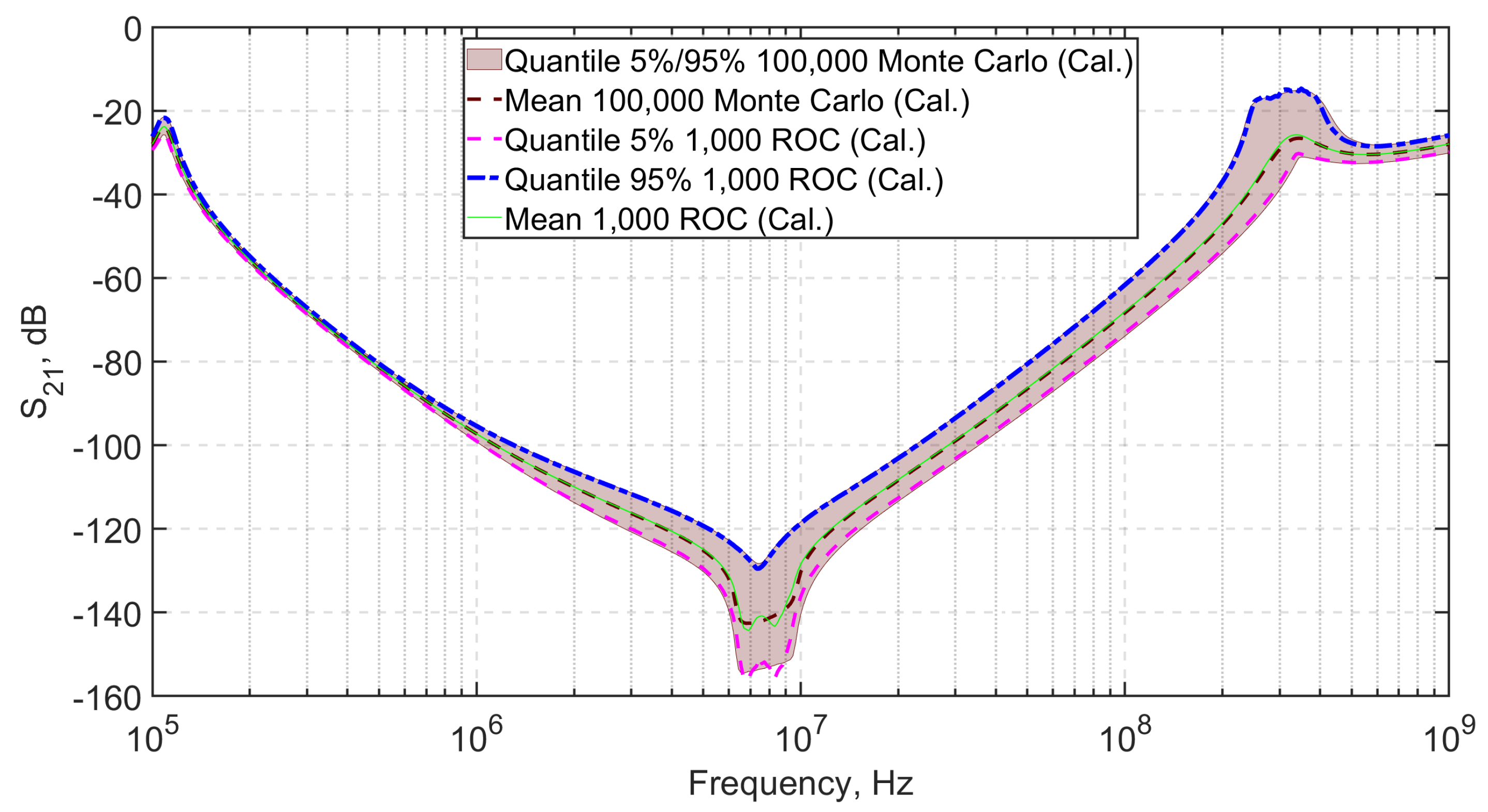
4.1. Assessing Filter Mean Trends and Extreme Values with ROC

The filter performance is given in Figure 11 and Figure 12 through S 21 parameter considering:
  • measurements (Exp.), respectively, for Channel #1/Channel #4 boards, with plain light red (Figure 11)/green (Figure 12) lines;
  • Spice model (Sim.) with dashed black line;
  • statistical data following analytical model (Calc.) with dark areas and curve.
Figure 11 gives an overview of the statistical dispersion of filter performances (via S 21 parameter) subject to random variations given in Table 1. S 21 minimum/maximum caliber is obtained from the Equation (7) (Calc. model) and 100,000 MC simulations. The deterministic configuration is validated through analytical (Calc.) model and nominal (i.e., using mean inputs in Table 1). Spice simulation (dashed black curve). One may notice this deterministic result agrees well with the mean trend extracted from MC simulations (dark red dotted curve). However, it is also to be noted that the statistical dispersion is important, particularly when considering the resonance area between 6 and 10 MHz.
Let us introduce the following terms (in decibels): P for the sought Performance, T for the selected Threshold, and S for the light notation of S 21 d B transmission.
Given the threshold targeted value ( T = 60 dB in Figure 11), the filter performance P may be assessed from the surface between the threshold and S representative curve as follows:
P f S f 2 = f S f 2 T S ( f ) df
where f S denotes the sampling frequency of the image sensor and f 2 the second cutting frequency where IL is greater than the threshold (T).
As previously illustrated with Channel #1, Figure 12 gives an overview of the comparison between measurements (Meas.), statistical MC calculations (Cal.) and deterministic Spice simulations (Sim.) considering Channel #4. The results also agree well considering statistical minimum/maximum caliber given by MC realizations (light green area) and measured data (light green curve).
The averaged S 21 parameter from MC simulations (dark green dotted curve) is in accordance with the deterministic results from Spice simulations (dashed black curve). One may also notice a huge dispersion of results (due to random assumptions of inputs) from 6 MHz to the highest frequencies.
Complementary to Figure 11 and Figure 12, Figure 13 and Figure 14 give an overview of the ROC capabilities considering:
  • the computation of S 21 mean, see, respectively, dark red dashed (MC) and light green plain curves (ROC) in Figure 13 for Channel #1;
  • the assessment of S 21 a l p h a = 5 %—and 1 α = 95%—quantiles, with dark red areas (MC) and pink/blue calibers (ROC).
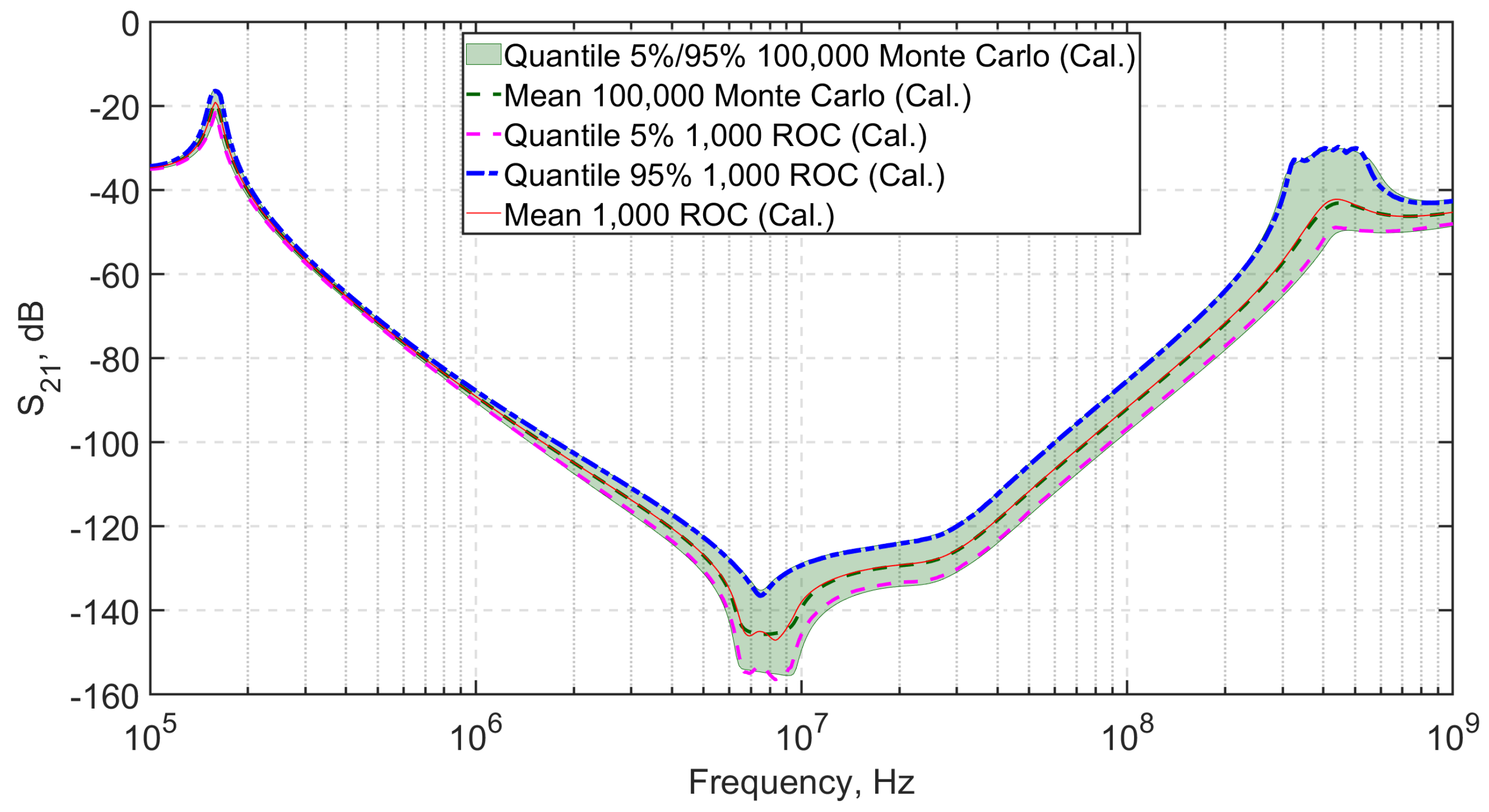
Figure 14 and Figure 15 show the very good quality of ROC reconstruction regarding the Channel #4 board for:
  • mean trend: S 21 average values are given from the whole dataset (MC reference with 100,000 simulations, dark green dashed curve) and computed from ROC sampling (1000 calculations, red curve), with an excellent agreement between MC and ROC (see Figure 14);
  • 5%/95% confidence intervals (CIs) quantiles: The green area (from 100,000 MC samples) agrees well with ROC calibers given by pink and blue dashed curves.
As pointed out with Channel #1, the results given for Channel #4 in Figure 15 show the excellent agreement between reference data and ROC computations. This is quantified through:
  • mean levels errors (green curve) lower than 4% (out of resonances),
  • quantiles levels (pink and blue curves) comprised between 0.3 and 10 percents of error (out of resonances).
As illustrated in Figure 16, the ROC reconstruction is fairly obtained comparatively to MC reference. Indeed, the relative gap between ROC and MC (100,000 realizations) is mainly below 4% (except resonances). The computation of 5% and 95% quantiles from ROC exhibits relative errors between 0.4 % and 10% (out of resonances).
Figure 17 shows the agreement between MC reference dataset (i.e., with 100,000 simulations) and ROC method (here still with 1000 realizations) for:
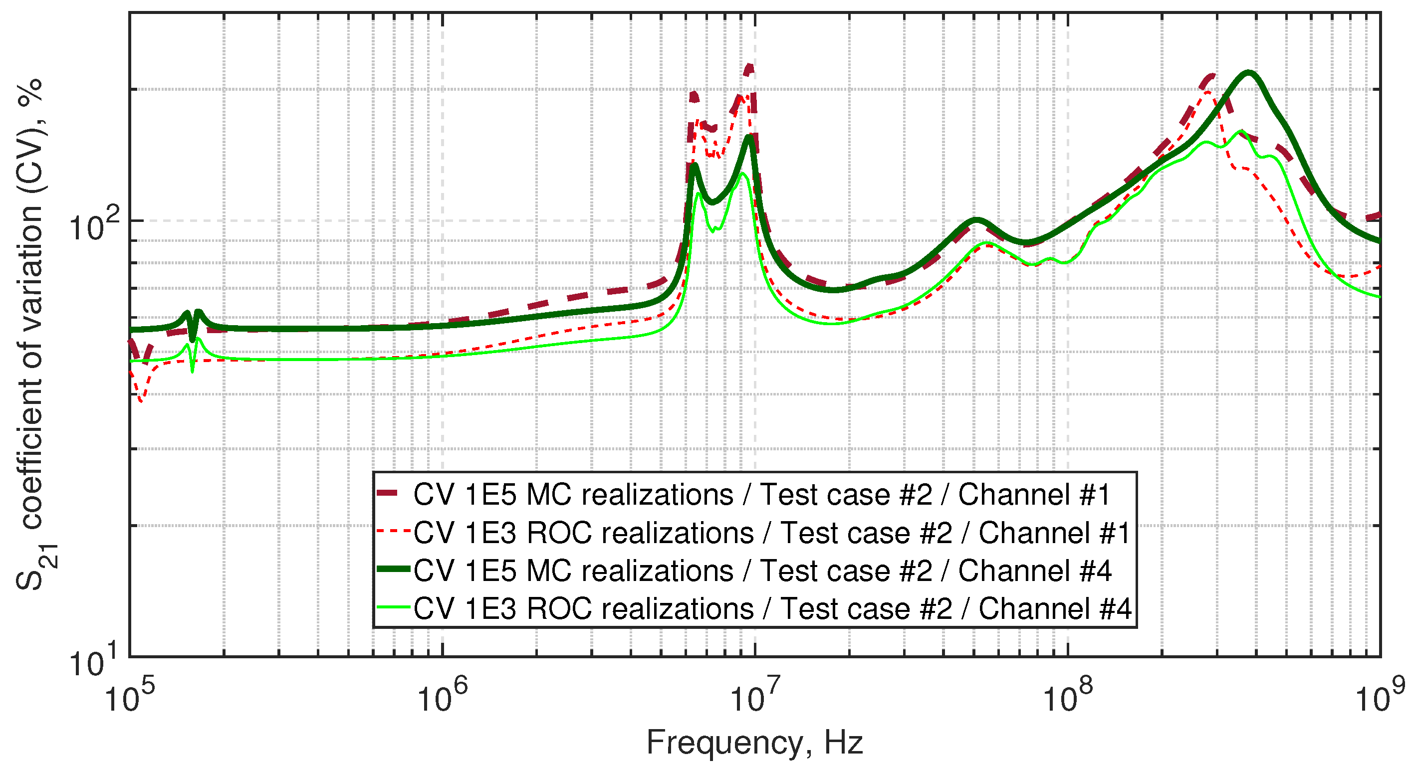
  • Channel #1 simulations (dark dashed and light dotted red curves, respectively, for MC and ROC techniques): The results represent the coefficient of variation C V (given as the ratio between S 21 standard deviation and mean at each frequency);
  • Channel #4 with S 21 C V simulations (dark bold and light plain green curves, respectively, for MC and ROC methods).
For both Channels #1 and #4, the results given in Figure 17 are in very good agreement between MC and ROC techniques. S 21 C V is useful to exhibit the most sensitive areas (frequency bandwidths). Thus, one may notice the sensitivity of the filter model is weak below a few MHz (for both Channels #1 and #4) with weak C V -levels (lower than 20% out of resonance). Apart from the resonance effects appearing around 10 MHz and 200 MHz, the sensitivity of the model is moderate but noticeable above 1 MHz (between 20% and 50%), as an indicator of the potential dispersion due to random variations. In the following, one may carry on this first approach of sensitivity analysis (SA) for test case #2 and considering alternative tools (Sobol’ indices).

4.2. Impact of Variable Sources and Loads: Results from Test Case #2

First of all, it is important to note that this part is dedicated to the influence of source and load variations considering Table 1, Table 2 and Table 3. In this context, four extra RVs are considered:
  • with variable serial resistance/self for source and parallel resistance/capacitor for load),
  • and still the two Channels #1 and #4 (test board).
As previously highlighted in Figure 17, CV is an interesting marker of the system sensitivity to random variations such as depicted in Table 1 and Table 2 for Test case #1. (Here, CV remains the Coefficient of Variation, i.e., the ratio of standard deviation over mean values for S 21 .)
Similarly to results in Figure 17, Figure 18 depicts the effect of random variations of inputs for Test case #2.
As expected, including random sources and loads involves huge effects when dealing with the filter sensitivity analysis:
  • Below 1 MHz, CVs are greater for both Channels #1 and #4 for concerning Test case #2 than for the first configuration (i.e., Test case #1): CVs here vary around 50%;
  • CV levels are higher above 1 MHz for Test case #2 comparatively to Test case #1: CVs are between 60% and 250%.
In order to enhance the huge difference existing between Test cases #1 and #2, the previous results and conclusions regarding the filter SA are, respectively, highlighted in:
  • Figure 19 for Channel #1: The results ( S 21 CVs) agree very well between reference MC (dark red curves) and ROC technique (light red curves).
  • Figure 20 for Channel #4: Again, the data from MC simulations (dark green curves) and the ROC method (light red curves) are in an excellent agreement.
It is to be noticed (Figure 19 and Figure 20) for a given frequency the gap existing between results in Test cases #1 and #2 are huge: At maximum 50% at lower frequency (i.e., below 1 MHz) and up to 100% for higher frequency (here around 200 MHz).
Considering results obtained in Figure 18 and Figure 20, one may expect the assessment of filter statistical performances should be more complex in Test case #2 than in Test case #1. In this framework, Figure 21 and Figure 22 have to be compared to the results obtained in Test case #1 (see Figure 13 and Figure 14, respectively, for board Channels #1 and #4).
The results obtained for Test case #2 and Channel #1 (Figure 21) show:
  • The excellent agreement between MC mean data (dark red curve) and the S 21 averaged trend given by the ROC technique (light green curve).
  • The good fit between extreme values (5% and 95% quantiles) given by MC reference and ROC (see, respectively, the dark red area and the pink/blue calibers). While the ROC results exhibit higher discrepancies for high quantiles, the ROC method still offers trustworthy confidence intervals to assess minimum/maximum trends.
In parallel to previous statements considering Channel #1, Figure 22 exhibits the very good match between MC results and ROC data (both for the assessment of mean value and quantiles). This section aimed at quantifying the interest of ROC methodology comparatively to the MC approach (in terms of accuracy and resources saving).
By introducing Test case #2, it has been demonstrated that the assumptions concerning source and loads (see Table 4) involved high levels of sensitivity (for both Channels #1 and #4). The next section will be dedicated to the influence of each random parameter in this process.

4.3. Ranking Most Influential Parameters from Sobol’ Indices

As mentioned before, this section is devoted to the study of the impact of each of the 10 (Test case #1) and 14 (Test case #2) random inputs as listed in Table 1, Table 2 and Table 3. Thus, the filter performance may be considered through P output for frequency bandwidth [ f S ; f 2 ] , with f S the sampling frequency of the image sensor (see Equation (10)) and f 2 is the first frequency following f S (i.e., f 2 > f S ; the first frequency f 1 where S 21 = T , with f 1 < f S , in not considered for our filter performance), where S 21 overcomes a given threshold. Obviously, the frequencies f S and f 2 may be freely assumed from a given threshold performance limit (T) and/or the system’s specifications (environmental constraints, electronic expectations, etc.).
In this context, we consider the particular case of f S = 10 MHz sampling and in the following, for the sake of simplicity, P will refer to P f S f 2 considering f S = 10 MHz and f 2 defined in Figure 11. This lays emphasis on the importance of the whole methodology proposed in this work. Indeed, since the stochastic formulation relies on a trustworthy analytical relation (Calc. results, see Equation (7)) assessing S 21 filter performance, two main advantages can be highlighted when computing the P output:
  • f 2 frequency can be assessed through the root search of function given from Equation (7). Here it was obtained as a formal computation of TS quantity. This can be achieved both depending on the T-value and independent from prior frequency choice (there is no need to provide high frequency sampling to improve the quality of f 2 search, but it requires higher computing time and resources).
  • As previously pointed out, Equation (7) is the cornerstone of this work, linking the physical interpretation that can be expected (e.g., influence of inputs, sensitivity analysis, etc.) to the efficient statistical calculations. Relation (10) may be computed following integration schemes (such as accurate Runge–Kutta methods).
The results in Table 4 refer to the ranking (Sobol’ indices) of:
  • most influential ( S i 1 % ) parameters (green colored): X 5 , X 1 and X 3 inputs, respectively, here are parasitic capacitance of bridge ( Z B ) self, parasitic inductances from upper ( Z U ) and downer ( Z D ) capacitors;
  • intermediate ( 0.1 % < S i < 1 % ) parameters (blue colored): X 4 , X 2 and X 10 inputs;
  • least influential ( S i 1 % ) parameters (red colored): X 6 X 9 inputs.
The data given through Sobol’ analysis for test case #1 show the great influence of parasitic elements (inductive and capacitive ones) modeled with RVs X 1 (ESL of Z U ), X 3 (ESL of Z D ) and X 5 (EPC of Z B ). In this case, this is independent from the threshold assumptions from T = 80 dB to T = 50 dB (data not shown here).
Sobol’ indices for test case #2 are given as follows:
  • Most influential ( S i 1 ) parameters (green colored):
    X 14 (EPC of Z C ), X 12 (ESL of Z V ), X 5 , X 1 and X 3 inputs;
  • Intermediate ( 0.1 < S i < 1 ) parameters (blue colored):
    X 13 , X 11 , X 4 and X 2 inputs;
  • Least influential ( S i 1 ) parameters (red colored):
    from X 6 to X 10 inputs.
In this case (here test case #2), the results are globally invariant from threshold T considering intermediate and least influential parameters. The comparison with results given in Table 4 is drastically different when introducing source and load variables. Indeed, the variations of source inductance and load capacitance (respectively, X 12 and X 14 inputs, as listed in Table 3) play major roles ( S 12 or S 14 Sobol’ indexes are greater than 34%).
Following the latter statement and in order to provide useful information considering first-order influential parameters, Figure 23 provides the normalized (from 0 to 1) Sobol’ indices with unity threshold sampling (here from 80 dB to 50 dB).
As previously highlighted, the results show the overwhelming importance of source and load variations, depending on T assumptions:
  • the source serial inductance ( X 12 ) is a key point up to T = 69 dB;
  • the load parallel capacitance ( X 14 ) plays a major role from T = 69 dB to T = 50 dB;
  • the influence of parasitic elements ( X 1 , X 3 and X 5 ) is noticeable with relative impact since normalized S i coefficients ( i = 1 , 3 , 5 ) vary from 0.05 to 0.12 , depending on T values;
  • other RVs might be withdrawn from the stochastic modeling since they only have an intermediate or lower effect when assumed.
The latter conclusions (see Figure 24) offer useful information to rank most influential parameters (test case #2) with respect to threshold levels:
  • T < 75 dB (high filter performance) requires to care about the source variability,
  • T > 65 dB (lower expectations from filter performance) needs to mostly consider the load influence,
  • 75 dB T 65 dB (intermediate area) exhibits both the importance of source inductance and load capacitance.

5. Conclusions

This article is devoted to the EMC performance of filtering components needed in the framework of optoelectronic sensing and space programs. The proposed methodology leans on the analytical formulation of an equivalent electrical model dedicated to computing Filter Efficiency. The model relies on the formalism of transfer [T]-matrix (Calc.); the analysis tool is then used to provide an original quantification of uncertainties. This work combines analytical (Calc.), simulation (Sim.) and experimental (Exp.) data to extract the equivalent Calc. model from an optimization step involving both measurements and simulations. Thus, the analytical model was validated through Spice simulations and Kron’s methodology adapted form LC-filter in [13].
The original ROC sampling method was successfully used, allowing the assessment of FE extreme performances (i.e., computing high quantiles’ levels, here 5% and 95% S 21 ). This leads to a limited number of simulations (here 100× speedup compared to golden standard MC realizations). The ROC dataset (here requiring 1000 well-chosen inputs) exhibits the frequency bandwidths with the maximum sensitivity (i.e., mainly where coefficient of variation, CV, is greater than 20%). The importance of source and load variability is quantified (test case #2): It is to be noticed that CV is greater than 40% for the whole frequency bandwidth (not only around resonances as previously pointed out for test case #1).
To evaluate the relative importance of one input to another, the analytical formulation offers reliable information, through Sobol’ indice extraction. The proposed methodology enables ranking most influential parameters with respect to filtering assumptions (threshold performance in dB).
Finally, the ROC method appears as a promising approach since ongoing works are nowadays leading to enriching filtering models. Thus, the works in [13] clearly exhibit, in this case (LC-filter), the potential importance of coupling between filter components.
The ROC method, similarly to MC sampling, has demonstrated its ability to handle a high number of RVs with a limited number of simulations. The proposed methodology (coupling MC sampling, ROC and Sobol’ indices) could be adapted, without any extra computing costs, to rank most influential parameters, this only from the ROC weighted dataset.

Author Contributions

Conceptualization: L.P. Methodology: L.P. Software: L.P. & S.L. Validation: L.P. & S.L. Formal analysis: L.P. Writing (original draft preparation): S.L. Writing (review and editing): L.P. Visualization: L.P. & S.L. Both authors have read and agreed to the published version of the manuscript.

Funding

This research received no external funding.

Conflicts of Interest

The authors declare no conflict of interest.

References

  1. Cours de Technologie Spatiale–Techniques & Technologie des Véhicules Spatiaux–Vol. 3-Charges Utiles: Aspects Techniques & Technologiques–Module 9: Techniques Optiques & Optoélectroniques–CNES; CNES: Toulouse, France, 2010. (In French)
  2. Nowosielski, L.; Wnuk, M.; Rychlica, J. Implementation of laboratory test stand for EMC filter attenuation measurement. In Proceedings of the 2019 International Symposium on Electromagnetic Compatibility-EMC EUROPE, Barcelona, Spain, 2–6 September 2019; pp. 504–507. [Google Scholar]
  3. Carobbi, C.F.; Lalléchère, S.; Arnaut, L.R. Review of Uncertainty Quantification of Measurement and Computational Modeling in EMC Part I: Measurement Uncertainty. IEEE Trans. Electromagn. Compat. 2019, 61, 1690–1698. [Google Scholar] [CrossRef]
  4. Lalléchere, S.; Carobbi, C.F.; Arnaut, L.R. Review of Uncertainty Quantification of Measurement and Computational Modeling in EMC Part II: Computational Uncertainty. IEEE Trans. Electromagn. Compat. 2019, 61, 1699–1706. [Google Scholar] [CrossRef]
  5. Pietrenko-Dabrowska, A.; Koziel, S. Reliable Surrogate Modeling of Antenna Input Characteristics by Means of Domain Confinement and Principal Components. Electronics 2020, 9, 877. [Google Scholar] [CrossRef]
  6. Aldoumani, M.; Yuce, B.; Zhu, D. Using the Variable Geometry in a Planar Inductor for an Optimised Performance. Electronics 2021, 10, 721. [Google Scholar] [CrossRef]
  7. Barakou, F.; Steennis, F.; Wouters, P. Accuracy and Reliability of Switching Transients Measurement with Open-Air Capacitive Sensors. Energies 2019, 12, 1405. [Google Scholar] [CrossRef] [Green Version]
  8. Malack, J.A.; Engstrom, J.R. RF Impedance of United States and European Power Lines. IEEE Trans. Electromagn. Compat. 1976, EMC-18, 36–38. [Google Scholar] [CrossRef]
  9. de Paulis, F.; Nisanci, M.H.; Orlandi, A.; Gu, X.; Rimolo-Donadio, R.; Baks, C.; Kwark, Y.; Archambeault, B.; Connor, S. Experimental validation of an 8 GHz EBG based common mode filter and impact of manufacturing uncertainties. In Proceedings of the 2013 IEEE International Symposium on Electromagnetic Compatibility, Denver, CO, USA, 5–9 August 2013; pp. 27–32. [Google Scholar]
  10. Huang, H. Development of Predictive Models for Electromagnetic Robustness of Electronic Components. Ph.D. Thesis, INSA Toulouse, Toulouse, France, 2015. [Google Scholar]
  11. CISPR 17, Methods of Measurement of the Suppression Characteristics of Passive EMC Filtering Devices; IEC International Standard; IEC: Geneva, Switzerland, 2011.
  12. MIL-STD-220 B. Test Method-Standard Method of Insertion Loss Measurement; Department of Defense-Military Standard. 24 January 2000. Available online: https://www.google.com.hk/url?sa=t&rct=j&q=&esrc=s&source=web&cd=&ved=2ahUKEwiegLfUuIfzAhWCFogKHZBHDkcQFnoECAwQAQ&url=http%3A%2F%2Feveryspec.com%2FMIL-STD%2FMIL-STD-0100-0299%2Fdownload.php%3Fspec%3DMIL-STD-220B_CHANGE-1.021983.pdf&usg=AOvVaw0t9qssWQegbeioPpW_IR64 (accessed on 17 August 2021).
  13. Stojanovic, M.; Lafon, F.; Fernandez-Lopez, P.; Op’t Land, S.; Perdriau, R. Modified Kron’s Method (MKME) for EMC optimization, applied to an EMC filter. In Proceedings of the APEMC International Symposium on Electromagnetic Compatibility, Shenzhen, China, 17–21 May 2016; pp. 782–784. [Google Scholar]
  14. Catani, J.P. Cours de Compatibilité Electromagnétique–Chap. 12: Filtrage des Circuits d’Alimentation; CNES: Toulouse, France, 1990. (In French)
  15. Lallechere, S. Advanced EMC Assessment of Composites Material: Monte Carlo Statistical Description with Spherical Inclusions and Improvement with SROM. Prog. Electromagn. Res. Lett. 2020, 88, 9–14. [Google Scholar] [CrossRef] [Green Version]
  16. Meiguni, J.; Zhang, W.; Soerensen, M.; Ghosh, K.; Hosseinbeig, A.; Patnaik, A.; Pommerenke, D.; Rollin, J.; Li, J.; Liu, Q.; et al. EMI Prediction of Multiple Radiators. IEEE Trans. EMC 2020, 62, 415–424. [Google Scholar] [CrossRef]
  17. Spath, H. Cluster Dissection and Analysis: Theory, FORTRAN Programs, Examples; Halsted Press: New York, NY, USA, 1985. [Google Scholar]
  18. Cannavo, F. Sensitivity analysis for volcanic source modeling quality assessment and model selection. Comput. Geosci. 2012, 44, 52–59. [Google Scholar] [CrossRef]
Figure 1. Electronic Architecture of a Space Detection Instrument.
Electronics 10 02301 g001
Figure 2. Principle of a voltage shifter: “From Low voltage to High voltage” design.
Electronics 10 02301 g002
Figure 3. Pi Filter Architecture and Conventional Notations.
Electronics 10 02301 g003
Figure 4. Serial (a) and parallel (b) impedances for RLC models.
Electronics 10 02301 g004
Figure 5. Power Filter Test Board (see four listed distinct channels).
Electronics 10 02301 g005
Figure 6. IL measurements on Test Board @ VNA (50 Ω in; 50 Ω out).
Electronics 10 02301 g006
Figure 7. Global methodology flowchart, from steps (AE). A: VNA measurements (Exp.) of S 21 parameter (Test Board, see results in Figure 6). (B): Retro-fitting of analytical reduced models (Calc.). (C): Spice simulation deterministic model (Sim.). (D): UQ through MC and ROC. (E): Statistical assessments.
Electronics 10 02301 g007
Figure 8. Description of Chain (or [ABCD] Transfer) matrix.
Electronics 10 02301 g008
Figure 9. IL simulations of Test Board with realistic mean impedances (1 Ω + 30 nH at Voltage shifter output; 300 Ω //30 pF at CCD sensor input).
Electronics 10 02301 g009
Figure 10. Illustration of ROC CDF reconstruction (orange dashed curve) compared to MC reference data (blue plain curve) through filter performance ( S 21 ) for Test case #1/Channel #1: At low frequency level f L = 400 kHz (left side) and at high frequency level f H = 800 MHz (right side). α = 10 % quantile and 1 α = 90% levels are given as an illustration, respectively, through pink and blue dotted levels.
Electronics 10 02301 g010
Figure 11. Filtering performances (statistics) from Test case #1/Channel #1 including: VNA measure-ments, simulations (Spice), MC calculations (analytical model).
Electronics 10 02301 g011
Figure 12. Filtering performances (statistics) from Test case #1/Channel #4 including: VNA measure-ments, simulations (Spice), MC calculations (analytical model).
Electronics 10 02301 g012
Figure 13. Filtering performances: 5%/95% confidence intervals from Test case #1/Channel #1 including MC samples and ROC calculations.
Electronics 10 02301 g013
Figure 14. Filtering performances: 5%/95% confidence intervals from Test case #1/Channel #4 including MC samples and ROC calculations.
Electronics 10 02301 g014
Figure 15. Relative gap between MC reference (100,000 data) and ROC simulations (1,000 realizations) from filtering performance statistics: 5%/95% confidence intervals and mean trend from Test case #1/Channel #4.
Electronics 10 02301 g015
Figure 16. Relative gap between MC reference (100,000 data) and ROC simulations (1000 realizations) from filtering performance statistics: 5%/95% confidence intervals and mean trend from Test case #1/Channel #1.
Electronics 10 02301 g016
Figure 17. S 21 Test cases #1: CVs from Channel #1 (red curves) and #4 (green curves).
Electronics 10 02301 g017
Figure 18. S 21 Test cases #2: CVs from Channel #1 (red curves) and #4 (green curves).
Electronics 10 02301 g018
Figure 19. S 21 CVs from Test cases #1 and #2 (Channel #1 configuration).
Electronics 10 02301 g019
Figure 20. S 21 CVs from Test cases #1 and #2 (Channel #4 configuration).
Electronics 10 02301 g020
Figure 21. Filtering performances: 5%/95% confidence intervals from Test case #2/Channel #1 including MC samples and ROC calculations.
Electronics 10 02301 g021
Figure 22. Filtering performances: 5%/95% confidence intervals from Test case #2/Channel #4 including MC samples and ROC calculations.
Electronics 10 02301 g022
Figure 23. Normalized first-order Sobol’ indices from Test case #2/Channel #1 (14 RVs).
Electronics 10 02301 g023
Figure 24. Normalized first-order Sobol’ indices from Test case #2/Channel #4 (14 RVs).
Electronics 10 02301 g024
Table 1. UQ with RVs Uniformly distributed involved for test case #1 (Channel #1).
# RVComponentTypeUnitMinimumMaximum
X 1 Z U ESLnH 0.180 0.420
X 2 Z U ESRm Ω 1842
X 3 Z D ESLnH 0.180 0.420
X 4 Z D ESRm Ω 1842
X 5 Z B EPC nF 0.270 0.630
X 6 Z B EPRk Ω 1.800 4.200
X 7 Z U Capacitor μ F 4.018 4.441
X 8 Z D Capacitor μ F 4.018 4.441
X 9 Z B Inductor μ H 0.950 1.050
X 10 Z B Resistorm Ω 3.4 7.8
Table 2. UQ with RVs Uniformly distributed involved for test case #1 (Channel #4).
# RVComponentTypeUnitMinimumMaximum
X 1 Z U ESLnH 0.180 0.420
X 2 Z U ESRm Ω 18.0 42.0
X 3 Z D ESLnH 0.012 0.028
X 4 Z D ESRm Ω 1.5 3.5
X 5 Z B EPC nF 0.300 0.700
X 6 Z B EPRk Ω 0.600 1.400
X 7 Z U Capacitor μ F 4.018 4.441
X 8 Z D Capacitor μ F 1.425 1.575
X 9 Z B Inductor μ H 0.855 0.945
X 10 Z B Resistorm Ω 3.4 7.8
Table 3. UQ with RVs Uniformly distributed involved for test case #2, in addition to RVs X 1 to X 10 in Table 1 and Table 2 (Channels #1 and #4).
# RVComponentTypeUnitMinimumMaximum
X 11 Z s o u r c e Resistor Ω 0.110
X 12 Z s o u r c e Serial inductancenH10100
X 13 Z l o a d Resistor Ω 1001000
X 14 Z l o a d Parallel capacitorpF10100
Table 4. Computed first-order Sobol’ indices ( S i , i = 1 , , 10 ) for Test case #1 (Channels #1 and #4, filter threshold T = −60 dB): ranking from most to least influential (respectively, from #1 to #10).
RankChannel #1/ T = 60 dBChannel #4/ T 60 dB
#1 S 5 = 43 % S 5 = 42 %
#2 S 1 = 38 % S 1 = 28 %
#3 S 3 = 18 % S 3 = 28 %
#4 S 4 < 1 % S 2 < 1 %
#5 S 2 < 1 % S 4 < 1 %
#6 S 10 < 1 % S 10 < 1 %
#7 S 9 1 % S 9 1 %
#8 S 8 1 % S 8 1 %
#9 S 7 1 % S 7 1 %
#10 S 6 1 % S 6 1 %
Publisher’s Note: MDPI stays neutral with regard to jurisdictional claims in published maps and institutional affiliations.

