Abstract
A new triple voltage boosting switched-capacitor multilevel inverter (SCMLI) is presented in this paper. It can produce 13-level output voltage waveform by utilizing 12 switches, three diodes, three capacitors, and one DC source. The capacitor voltages are self-balanced as all the three capacitors present in the circuit are connected across the DC source to charge it to the desired voltage level for several instants in one fundamental cycle. A detailed comparative analysis is carried to show the advantages of the proposed topology in terms of the number of switches, number of capacitors, number of sources, total standing voltage (TSV), and boosting of the converter with the recently published 13-level topologies. The nearest level control (NLC)-based algorithm is used for generating switching signals for the IGBTs present in the circuit. The TSV of the proposed converter is 22. Experimental results are obtained for different loading conditions by using a laboratory hardware prototype to validate the simulation results. The efficiency of the proposed inverter is 97.2% for a 200 watt load.
1. Introduction
In recent times, multilevel inverters (MLIs) have been used as a potential solution for DC to AC conversion for various applications such as renewable energy conversion systems, high power drives, a high-voltage direct current (HVDC) transmission system, a distributed power generation system, etc. The main advantages of MLIs are lower dv/dt stress, higher operating voltage with lower rating devices, and near to sinusoidal output voltage, which in turn reduces total harmonic distortion (THD) and fault-tolerant capability [1,2,3]. Conventional MLIs such as the neutral point clamped (NPC) inverter, flying capacitor (FC) inverter, cascaded H-bridge (CHB) inverter, and modular multilevel converter (MMC) have replaced the conventional two-level inverter for medium and high voltage applications [4,5]. However, these conventional MLIs require more components and more complex control circuitry due to voltage balancing issues with an increased number of levels at the output voltage.
To overcome these issues, researchers have proposed a self-balanced switched-capacitor multilevel inverter (SCMLI), which can synthesize the desired voltage levels at the output using fewer components and reduced control complexity [6,7,8,9,10,11,12]. Several SCMLIs has been presented by researchers utilizing fewer components to realize the desired multilevel output voltage. A seven-level inverter is proposed in [13], which utilizes 10 switches and one capacitor to produce 1.5 times voltage gain. Authors in [14] have used 12 switches and two capacitors to generate seven-level output voltage with increased voltage gain. Recently, several high gain SCMLIs were proposed which are capable of producing 13-level output voltage [15,16,17,18,19,20,21]. Four DC sources and 10 switches are used to produce 13-level output voltage in [18] with unity voltage gain. To improve the voltage gain and to reduce the number of sources, [22] uses only one DC source for producing 1.5 times voltage boosting, while [16] uses two sources to achieve dual voltage boosting with an increased number of switches. In [23] a high-voltage boosting of six is achieved, but the number of switches used in the circuit is twenty-nine with a total standing voltage (TSV) of 34. To reduce the number of switches, the authors in [19] used 19 switches for generating voltage boosting of six, but the TSV of the inverter circuit increased to 39. A detailed review on the recently published multilevel inverter topologies to find the most suitable applications with reduced device count is published in [7,8,9,10,11,12]. In the case of lower solar PV voltages, a high gain DC–DC converter along with multilevel inverter can be used to boost the PV voltage for obtaining desired output voltage for grid integration [24,25,26].
In this paper a triple voltage gain SCMLI topology is proposed with reduced component count and reduced TSV. The number of switches used in the proposed circuit is 12, with reduced TSV to 22. A simpler NLC based algorithm is used to generate switching pulses for IGBTs employed in the proposed circuit. The main objectives of the proposed topology are as follows;
- (a)
- A 13-level output voltage is synthesized with 11 switches and one DC source.
- (b)
- The proposed topology provides triple voltage boosting at the output.
- (c)
- Total standing voltage (TSV) of the proposed topology has significantly reduced.
- (d)
- Negative voltage levels are generated without using an H-bridge.
- (e)
- All three capacitor voltages are self-balanced, hence control circuitry is simple.
The proposed circuit configuration, its working during different modes of operation, and charging–discharging states of the self-balanced capacitors are discussed in detail in Section 2. Capacitor selection criteria, power loss analysis, and switching algorithm are discussed in Section 3. Section 4 presents the comparative analysis of the proposed SCMLI with recently published 13-level MLIs in terms of component used, sources used, gain, and TSV. Section 5 presents the experimental results which were conducted to verify its feasibility and performance under different loading conditions. Finally, conclusions are presented in Section 6.
2. Proposed Switched-Capacitor Topology
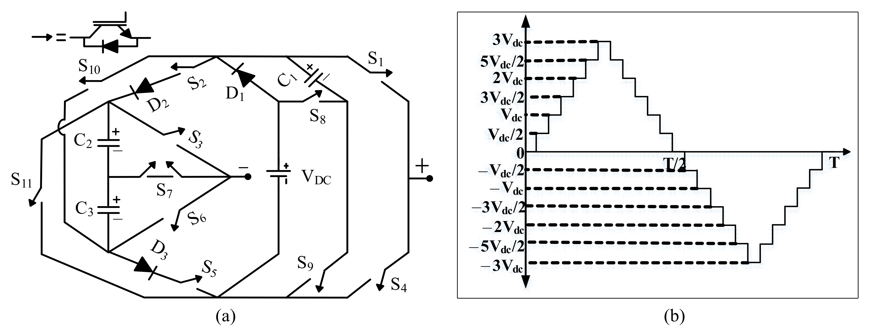
The topology and output voltage waveform for the proposed 13-level SCMLI is shown in Figure 1. An elaborate discussion on the proposed SCMLI is presented as follows.
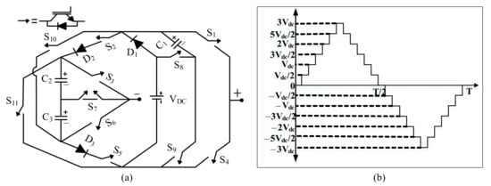
Figure 1.
Proposed topology: (a) circuit diagram, (b) 13-level output voltage.
2.1. Circuit Analysis
Figure 1a shows the proposed SCMLI topology comprising one bidirectional switch (S7), ten unidirectional switches (S1, S2, S3, S4, S5, S6, S8, S9, S10, S11), three diodes (D1, D2, D3), three capacitors (C1, C2, C3), and one DC source (Vdc). The 13-level output voltage waveform with triple voltage boosting is shown in Figure 1b. The capacitors are self-balanced and become charged to desired voltage levels for several instants during the fundamental cycle using the series-parallel voltage balancing principle. The capacitor C1 is charged to Vdc, and the remaining two capacitors are charged to Vdc/2 to achieve 13 output voltage levels as 0, ±Vdc/2, ±Vdc, ±3Vdc/2, ±2Vdc, ±5Vdc/2, ±3Vdc.
2.2. Description of Voltage Levels
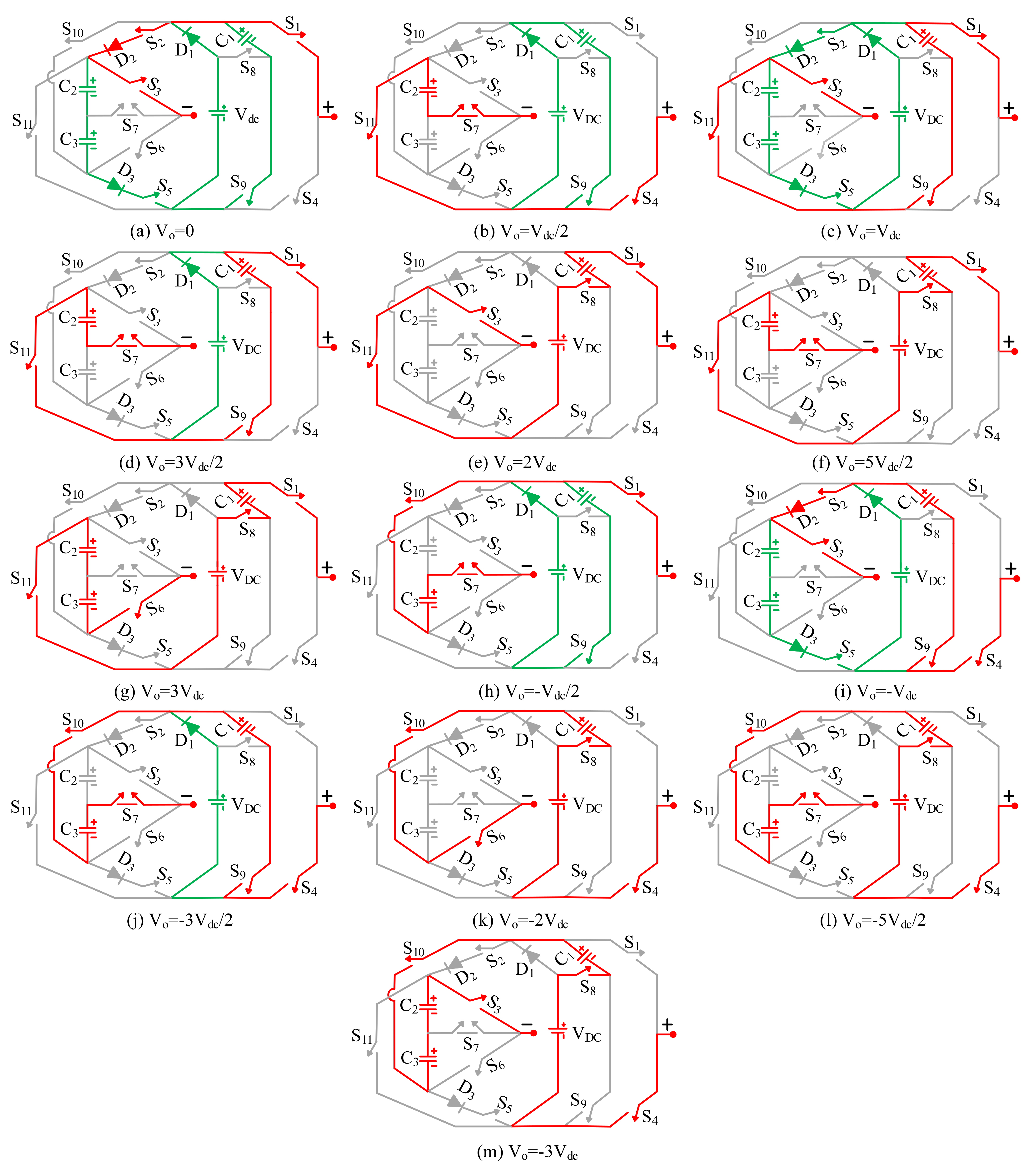
Table 1 shows the switching states of the proposed SCMLI. It also shows the capacitors charging and discharging states. The conduction states of the proposed topology during the positive and negative half cycle are shown in Figure 2. Red lines represent the conduction path to the load, and green lines represent the capacitor charging path. The zero-voltage state is produced by switching on S1, S2, S3, while S5 and S9 are used for charging the circuit capacitors as shown in Figure 2a. Voltage level +Vdc/2 is obtained through the capacitor C2 voltage, and at the same time, capacitor C1 is charged to source voltage as shown in Figure 2b. Voltage level +Vdc is obtained through capacitor C2 and C3 voltages, at the same time all the three capacitors are charged to their respective voltage values as shown in Figure 2c. Voltage level +3Vdc/2 is obtained through capacitor C1 and C2 voltages, as shown in Figure 2d. Voltage level +2Vdc is obtained through capacitor C1 voltage and Vdc, as shown in Figure 2e. Voltage levels +5Vdc/2 is obtained through capacitor C1, C2 voltages, and Vdc, as shown in Figure 2f. Voltage level +3Vdc is obtained through capacitors C1, C2, C3 voltages, and Vdc, as shown in Figure 2g. During the negative half-cycle, voltage level −Vdc/2 is obtained through capacitor C3 voltage, as shown in Figure 2h. Voltage level −Vdc is obtained through Vdc, as shown in Figure 2i. Voltage level −3Vdc/2 is obtained through Vdc and capacitor C3 voltage, as shown in Figure 2j. Voltage level −2Vdc is obtained through Vdc and capacitor C1 voltage, as shown in Figure 2k. Voltage level −5Vdc/2 is obtained through Vdc, capacitor C1, and C3 voltages, as shown in Figure 2l. Voltage level −3Vdc is obtained through Vdc, capacitor C1, C2, and C3 voltages, as shown in Figure 2m.

Table 1.
Switching table and capacitor states for the proposed 13-level inverter.
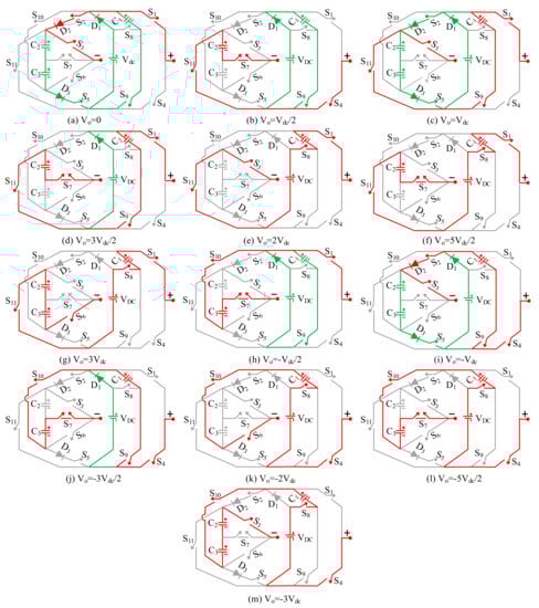
Figure 2.
Conduction states of the proposed topology: (a) zero voltage level, (b–g) positive half-cycle (h–m) negative half-cycle.
3. System Design and Component Selection
In this section, capacitor design criteria, nearest-level control technique, and power loss analysis of the proposed converter are discussed.
3.1. Capacitor Design
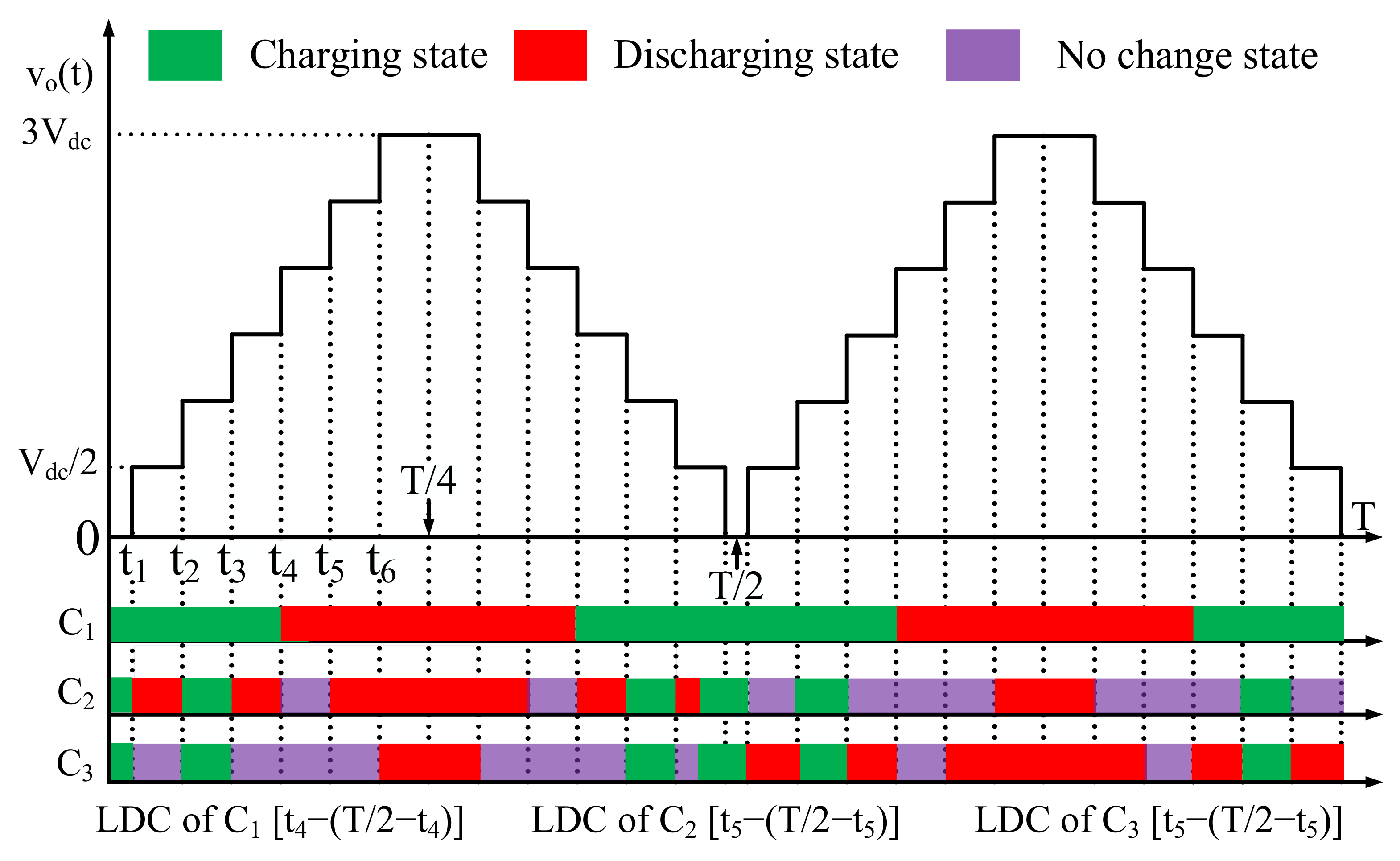
The proposed SCMLI topology utilizes three capacitors C1, C2, and C3 along with one DC source to generate the 13-level output voltage. All three capacitor voltages are self-balanced to the desired voltage level through the parallel connection of the source to the capacitor at different instants of time during the fundamental switching cycle. C1 voltage is maintained equal to the source voltage (Vdc) while C2 and C3 are charged to half of the source voltage (Vdc/2). The charging and discharging durations for C1, C2, and C3 are shown in Figure 3. The optimal value of capacitors can be calculated by considering the largest discharging cycle (LDC) of the capacitors and the type of loading current. The expression for the total discharge of capacitor C1 during the LDC interval [t4, T/2 − t4] is calculated as,
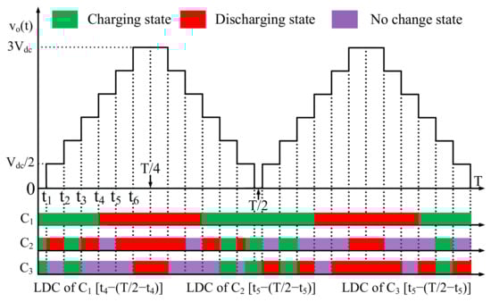
Figure 3.
Charging and discharging pattern of circuit capacitors C1, C2 and C3.
The longest discharging interval of capacitor C2 and C3 are equal. Hence the expression for the total discharge of capacitor C2 and C3 during the longest discharging interval [t5, T/2 − t5] can be expressed as,
From Equations (1) and (2), the values of C1, C2 and C3 can be evaluated as,
By considering ∆Vc equal to 10% of the corresponding capacitor voltage magnitude the corresponding values of ∆Vc1, ∆Vc2 and ∆Vc3 will be equal to 10 V, 5 V and 5 V respectively.
The values of t1, t2, t3, t4, t5 and t6 can be calculated as follows,
By using Equation (6), t1, t2, t3, t4, t5 and t6 is calculated as 0.53 ms, 1.09 ms, 1.67 ms, 2.32 ms, 3.10 ms and 4.3 ms, respectively.
By considering a purely resistive load of 50 Ω the load current can be expressed,
The output voltage peak is 300 V and load resistance is 50 Ω then the peak value of load (Im) will be 6 A.
The solution of Equation (3) for calculating the exact value of capacitor C1 is given as,
The solution of Equation (4) for calculating the exact value of capacitor C2 and C3 is given as,
After putting all corresponding values into Equation (8) the final solution of C1 comes out to be 2880 µF. The nearest available value of the capacitor in the lab is 4700 µF, that is why it is chosen for experimental purposes. After putting all corresponding values in Equation (9) the final solution of C1 and C3 comes out to be 4383 µF. The nearest available value of capacitor in the lab is 4700 µF, that is why it is chosen for experimental purposes.
3.2. Power Loss Analysis
The power loss analysis of the proposed SCMLI provides capacitor charging loss, conduction loss, and switching loss occurring in the system. The conduction loss is due to the voltage drop across the switch when the load current flows through the circuit. The capacitor charging current is responsible for capacitor charging power loss.
3.2.1. Capacitor Charging Power Loss ()
During the charging process of the capacitor, the charging current flows through the capacitor whose magnitude depends upon the voltage difference between the present value of the capacitor voltage and the desired value of the capacitor voltage. The power loss associated with capacitor charging is expressed as:
where m is the number of capacitors present in the circuit, ∆Vcm,i is the capacitor voltage ripple in the ith interval cycle. ∆Vcm can be calculated as per the following equation,
where, duration [t0, td] is the largest discharging cycle, and ic is the capacitor charging current.
3.2.2. Conduction Loss Due to Load Current
The conduction loss in an IGBT is caused due to load current flowing through it, which is expressed as,
where Von_sw and Ron_sw are the forward voltage drop and on-state resistance of the switch. I av_sw and Irms_sw are the respective average and RMS values of switch current.
3.2.3. Switching Loss (PSW)
Switching loss occurs during the switching process of IGBTs. It is a turn-on and turn-off loss that can be calculated on the basis of overlap in switch voltage and current at the switching instants. The switching power loss during the turn-on process is computed as:
After solving Equation (8) Psw_on can be written as:
Likewise, Psw_off can be written as:
Likewise, Vstd is the withstanding voltage of the switch, is the current flowing through the switch during turn-on time, is the current flowing through the switch during turn-off time, ton and toff is the turn-on and turn-off time of the switch, respectively.
The total switching power loss during one switching ON and OFF period is calculated as:
3.3. Nearest Level Control (NLC)
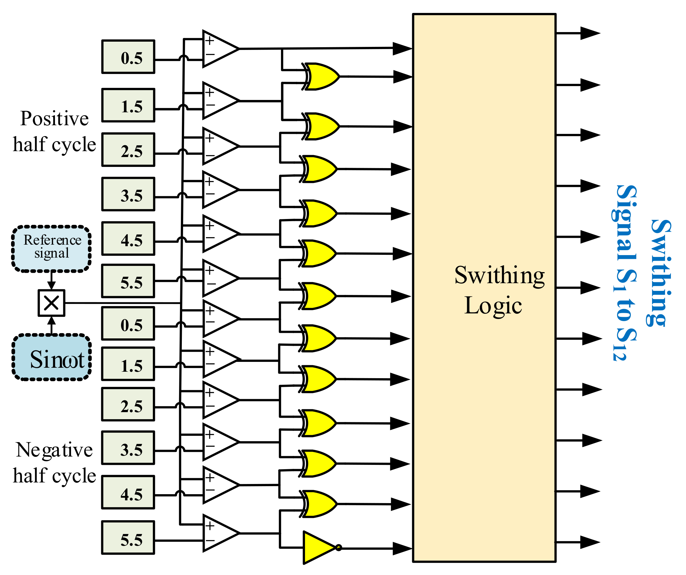
Numerous modulation schemes have been tested and used for multilevel inverters. The nearest level control is a low switching frequency PWM technique in which there is less complexity in implementation for a higher number of levels. NLC is used here for the proposed topology to control the switches so that the desired output waveform is obtained. In NLC, the reference sinusoidal waveform is compared with the desired output waveform to obtain a sampled waveform. The waveform generated is then rounded off to the nearest level and compared according to the switching logic given in Table 1 to produce switching signals for the corresponding IGBTs. The comparison of reference sine wave with the desired output voltage levels is shown in Figure 4 [16]. The working principle of the NLC is shown in Figure 5.
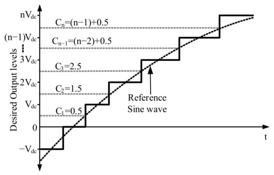
Figure 4.
Sampled reference signal.
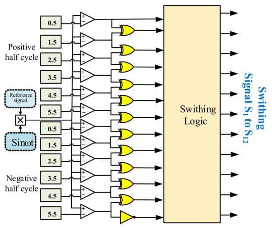
Figure 5.
Nearest level control logic for switching pulse generation.
4. Comparative Analysis
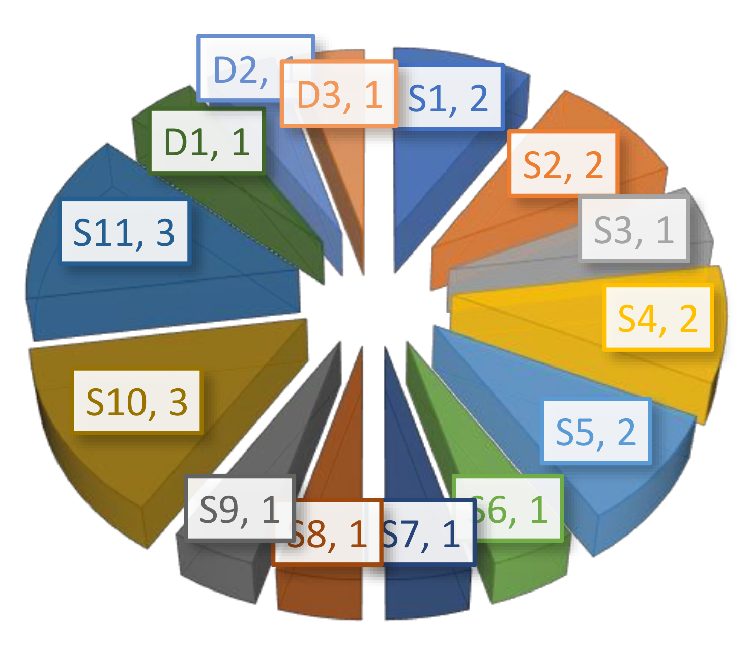
The comparative analysis of the proposed 13-level inverter with recently published 13-level topologies is carried out to show its advantages over other existing topologies. Table 2 shows the detailed comparative analysis on the basis of the number of switches (Nsw), number of diodes (Nd), number of DC sources (Ns), the total number of switching components (NT), number of capacitors (Nc), voltage gain of the converter and TSV. The ratio of the number of levels and total switching components is analyzed and compared. The proposed topology requires a minimum number of switches as compared to other topologies, which have a gain of three or more, as presented in Table 2. The number of switches used is 10 in the case of [11], but the gain is only one. In [13], the number of switches is 10, but it also requires 10 diodes and five capacitors to produce a gain of six. In [9] the number of switches used is 14 with two DC sources to produce a gain of two. In [10] the number of switches is the same as [9] with a reduced number of sources, but the number of capacitors used has increased to four. References [12,14,15] produce higher gain but require more switches as compared to the proposed inverter. Moreover, the TSV of these topologies are higher than the proposed topology. The proposed inverter has the lowest TSV amongst the compared topologies, which is only 22. Figure 6 shows the total standing voltage across individual switches and diodes.
Table 2.
Comparative analysis of the proposed MLI with recent 13-level topologies.
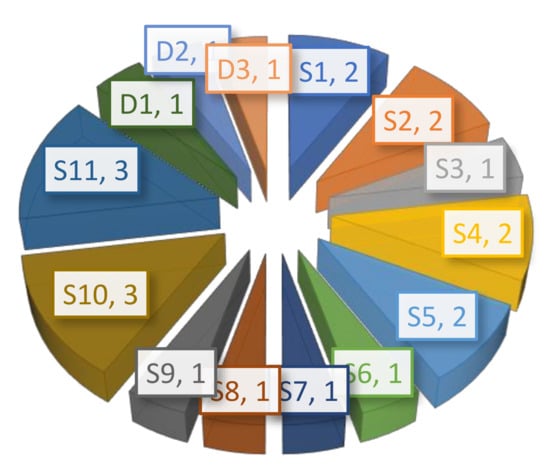
Figure 6.
Total standing voltage of different switches and diodes.
5. Results and Discussion
In this section, simulation results and hardware results of the proposed 13-level inverter topology is presented for different loading conditions.
5.1. Simulation Results
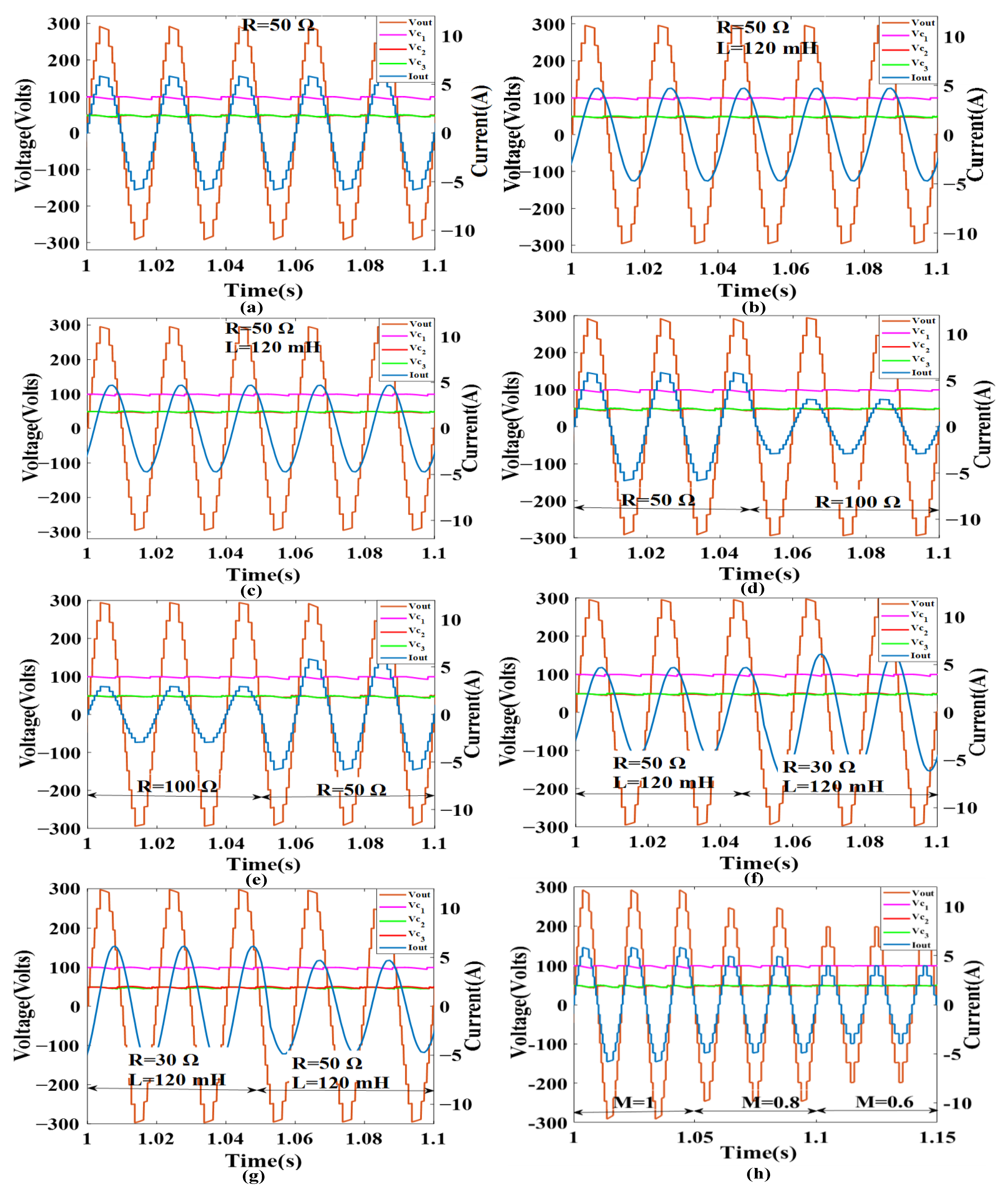
The simulation results of the proposed topology are shown in Figure 7. Output voltage, capacitor C1 voltage (Vc1), capacitor C2 voltage (Vc2), capacitor C3 voltage (Vc3) and load current waveform of the proposed 13-level inverter for the purely resistive load (R = 50 Ω) is shown in Figure 7a. Figure 7b shows the output voltage Vc1, Vc2, Vc3 and load current waveform for series connected R and L of load (R = 50 Ω, L = 120 mH). The effect of load change on load voltage, Vc1, Vc2, Vc3 and load current is shown in Figure 7c, when load is changed from R to series connected R and L load. For varying purely resistive load as well as for series connected R and L load, the output voltage, Vc1, Vc2, Vc3 and load current is shown in Figure 7d–g. The effect of change in modulation index on the number of levels at the output voltage is shown in Figure 7h. Simulation parameters are shown in Table 3.
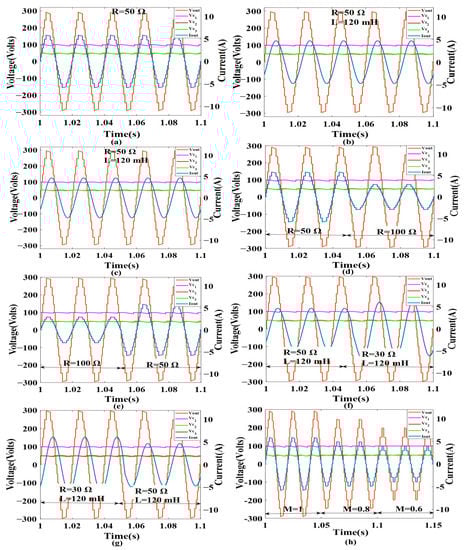
Figure 7.
Output voltage, capacitor C1 voltage Vc1, capacitor C2 voltage Vc2, capacitor C3 voltage Vc3, and load current waveform of the proposed 13-level inverter for (a) resistive load of 50 Ω (b) for series connected R and L load (R = 50 Ω, L = 120 mH) (c) change in load from resistive (R = 50 Ω) to series connected R and L load (R = 50 Ω, L = 120 mH) (d) reduction in resistive load from 50 Ω to 100 Ω (e) increase in resistive load from 100 Ω to 50 Ω (f) increase in series connected R and L load from (R = 50 Ω, L = 120 mH) to (R = 30 Ω, L = 120 mH) (g) reduction in series connected R and L load from (R = 30 Ω, L = 120 mH) to (R = 50 Ω, L = 120 mH) (h) change in modulation from M = 1.0 to M = 0.8 to M = 0.6.
Table 3.
Simulation parameters.
5.2. Hardware Results
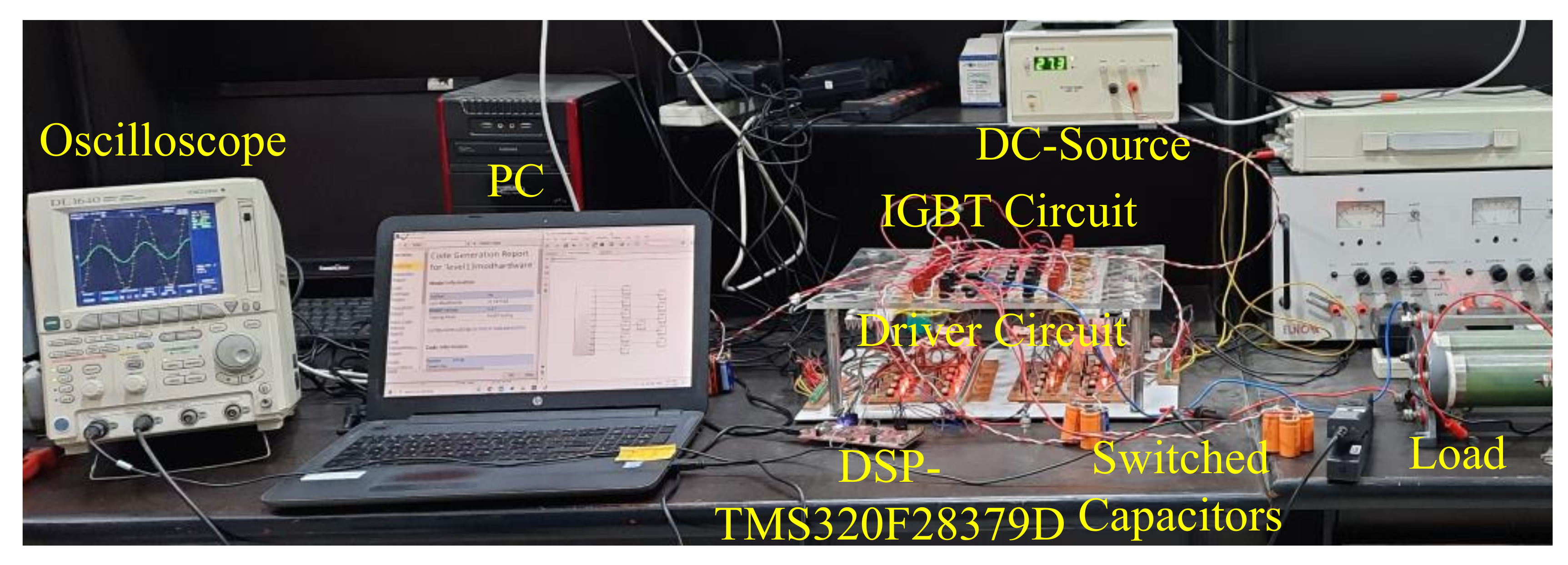
The detailed performance analysis of the proposed 13-level inverter is experimentally validated by using a hardware prototype. It is made with twelve insulated gate bipolar transistor (IGBT) (FGA25N120) and TLP-250 based gate driver circuit for providing gating signals to individual IGBTs. Switching signals are provided using a fundamental frequency switching scheme i.e., nearest level control (NLC). The NLC scheme is implemented using a digital signal processor (DSP) (TMS320F28379D) for the proposed inverter. A FLUKE make 435-II power analyzer is used for measuring experimental % THD of the proposed MLI. Experimental parameters are shown in Table 4. The experiment setup is shown in Figure 8.
Table 4.
Parameters for experimental validation.

Figure 8.
Experiment setup.
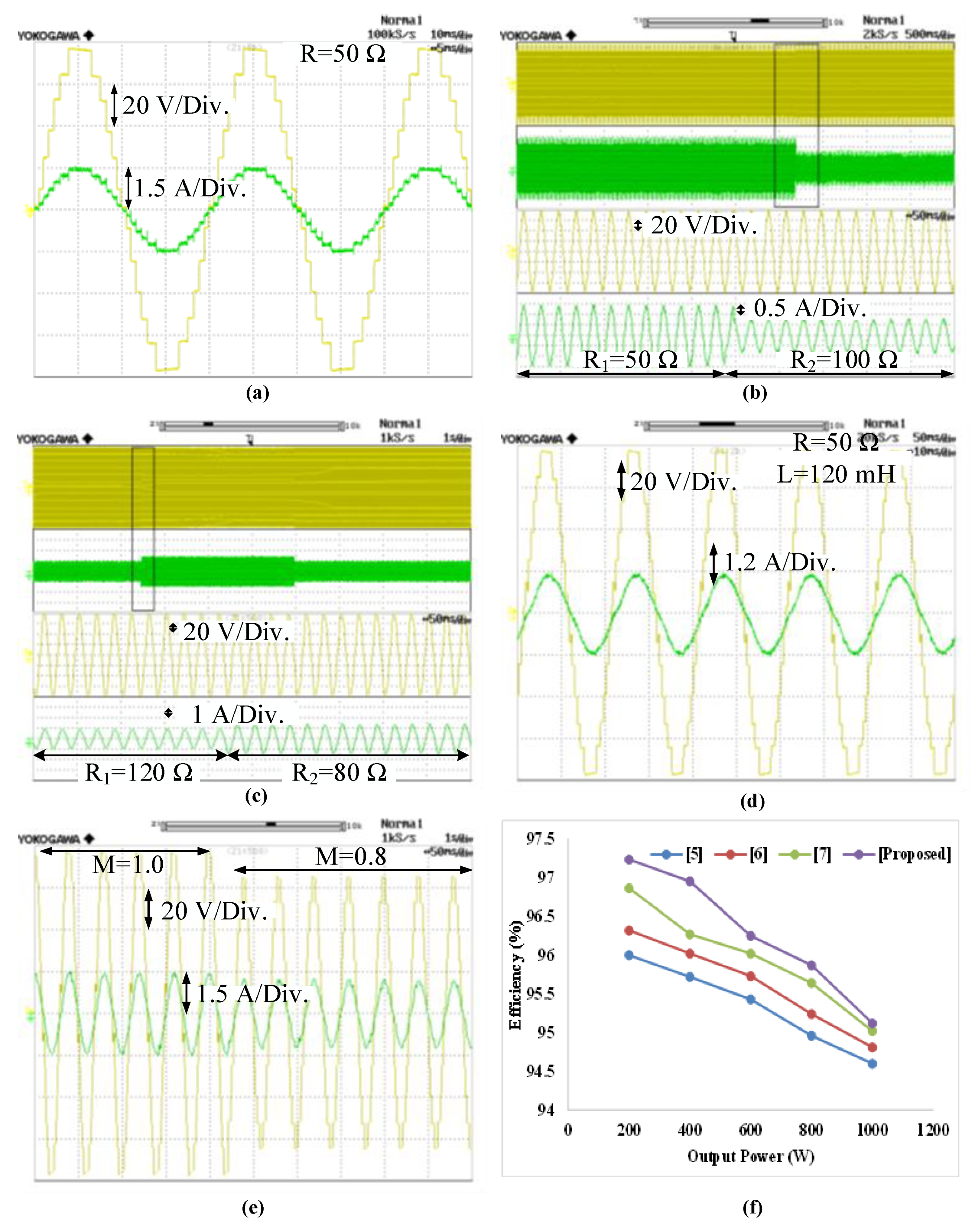
The 13-level output voltage with a peak voltage of 75 volts and a current peak of 1.5 A for R (50 Ω) load is shown in Figure 9a. When the load is suddenly changed from 50 Ω to 100 Ω, the magnitude of load current changes from 1.5 A to 0.75 A as the load is reduced to half as shown in Figure 9b. Load is also changed from 120 Ω to 80 Ω to validate the performance of the proposed converter which is shown in Figure 9c.
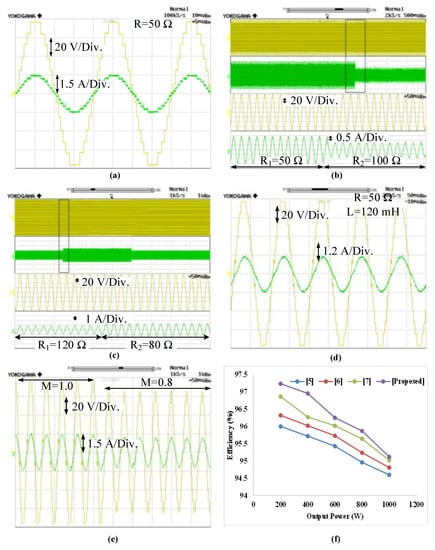
Figure 9.
Output voltage and current waveform of the proposed 13-level inverter: (a) R load, (b) during load resistance changed from 50 Ω to 100 Ω, (c) during load resistance changed from 120 Ω to 80 Ω, (d) with RL load, (e) change in modulation from M = 1.0 to M = 0.8, (f) efficiency comparison at different loading conditions.
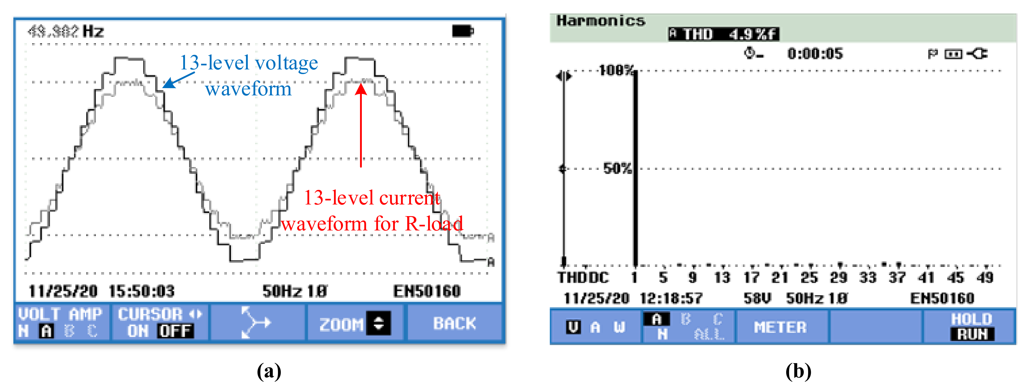
The experimental results are also obtained for RL load, as shown in Figure 9d. By changing the modulation index (M) from 1 to 0.8, the number of levels in the output voltage reduces from 13 to 11 as shown in Figure 9e. If we keep on reducing the value of M, then the number of levels will decrease accordingly. The efficiency curve of the proposed topology is plotted for different loads, and it is also compared with the other 13-level topologies. Figure 9f shows the efficiency curve of the proposed converter for different loading conditions. It is 97.2% when the loading of the inverter is 200 W. It reduces slightly when the load is increased from to 200 W to 1000 W. THD result of the generated output voltage is obtained using a FLUKE 435-II power quality analyzer. Figure 10a shows the generated 13-level output voltage waveform measured through a power quality analyzer. The measured %THD of the output voltage waveform is 4.9%. The %THD result is shown in Figure 10b.
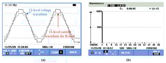
Figure 10.
Output voltage and current waveform (a) 13-level voltage and current (b) %THD of the generated output voltage.
6. Conclusions
In this paper, a 13-level switched-capacitor MLI using one bidirectional switch and 10 unidirectional switches, one DC source, three diodes, and three capacitors is proposed and analyzed in detail. The proposed MLI possesses inherent self-voltage balancing capability, which eliminates the need for a complex control circuit for capacitor voltage balancing. A detailed simulation analysis of the proposed 13-level converter is undertaken using MATLAB software. Performance of the proposed MLI is validated experimentally with R and RL loads using the developed laboratory prototype, and a satisfactory operation is observed. It is also tested for different types of loading condition along with sudden load change and change in modulation index (M). TSV of the proposed converter is 22, which is significantly less than other existing topologies. The gain of the proposed converter is three with reduced switch count and reduced TSV. The output voltage THD of the proposed inverter is 4.9% which is within limits as per IEEE-519 standard. The maximum efficiency is 97.2% for a 200 W load.
Author Contributions
Conceptualization, M.T. (Mohammad Tayyab), A.S., M.T. (Mohd Tariq) and M.R.H.; Formal analysis, M.T. (Mohammad Tayyab), A.S., I.K., M.T. (Mohd Tariq), M.R.H. and S.M.; Funding acquisition, M.T. (Mohd Tariq) and W.A.; Investigation, M.T. (Mohammad Tayyab), A.S., I.K., M.T. (Mohd Tariq), M.R.H., S.M. and W.A.; Methodology, M.T. (Mohammad Tayyab), A.S., I.K., M.T. (Mohd Tariq), M.R.H. and W.A.; Project administration, M.T. (Mohd Tariq) and W.A.; Supervision: A.S. and M.T. (Mohd Tariq); Writing—original draft, M.T. (Mohammad Tayyab) and A.S.; Writing—review and editing, I.K., M.T. (Mohd Tariq), M.R.H. and W.A. All authors have read and agreed to the published version of the manuscript.
Funding
The authors extend their appreciation to the Deputyship for Research Innovation, Ministry of Education in Saudi Arabia for funding this research work through the project number “375213500”.
Acknowledgments
The author (Mohammad Tayyab) acknowledges the financial support provided by CSIR under SRF category (09/112(0569)/2017-EMR-I). The authors also acknowledge the financial support provided from the Collaborative Research Grant Scheme (CRGS) Projects CRGS/MOHD TARIQ/01 and CRGS/MOHD TARIQ/02 sponsored by the Capability Systems Centre, UNSW, Canberra to the Hardware-In-the-Loop (HIL) Lab, Department of Electrical Engineering, Aligarh Muslim University, India and the technical support provided by the Non-Conventional Energy (NCE) Lab, Department of Electrical Engineering, Aligarh Muslim University, India.
Conflicts of Interest
The authors declare no conflict of interest.
References
- Ye, Y.; Chen, S.; Wang, X.; Cheng, K.W.E.E. Self-Balanced 13-Level Inverter Based on Switched Capacitor and Hybrid PWM Algorithm. IEEE Trans. Ind. Electron. 2021, 68, 4827–4837. [Google Scholar] [CrossRef]
- Tayyab, M.; Sarwar, A.; Tariq, M.; Chakrabortty, R.K.; Ryan, M.J. Hardware-in-the-Loop Implementation of Projectile Target Search Algorithm for Selective Harmonic Elimination in a 3-Phase Multilevel Converter. IEEE Access 2021, 9, 30626–30635. [Google Scholar] [CrossRef]
- Hussan, R.; Sarwar, A.; Siddique, M.D.; Mekhilef, S.; Ahmad, S.; Sharaf, M.; Zaindin, M.; Firdausi, M. A Novel Switched-Capacitor Multilevel Inverter Topology for Energy Storage and Smart Grid Applications. Electronics 2020, 9, 1703. [Google Scholar] [CrossRef]
- Panda, K.P.; Bana, P.R.; Panda, G. A Reduced Device Count Single DC Hybrid Switched-Capacitor Self-Balanced Inverter. IEEE Trans. Circ. Syst. II Express Briefs 2021, 68, 978–982. [Google Scholar] [CrossRef]
- Tayyab, M.; Sarwar, A. Submodule Capacitor voltage balancing of Modular Multilevel Converter. In Proceedings of the 2019 International Conference on Electrical, Electronics and Computer Engineering (UPCON), Aligarh, India, 8–10 November 2019; Volume 2, pp. 2–6. [Google Scholar]
- Tayyab, M.; Sarwar, A. Level Shifted Carrier-Based Pulse Width Modulation for Modular Multilevel Converter. In Renewable Power for Sustainable Growth; Lecture Notes in Electrical Engineering; Springer: Singapore, 2021; Volume 723, pp. 639–646. [Google Scholar] [CrossRef]
- Srinivasan, G.; Rivera, M.; Loganathan, V.; Ravikumar, D.; Mohan, B. Trends and Challenges in Multi-Level Inverter with Reduced Switches. Electronics 2021, 10, 368. [Google Scholar] [CrossRef]
- Khan, M.Y.A.; Liu, H.; Yang, Z.; Yuan, X. A Comprehensive Review on Grid Connected Photovoltaic Inverters, Their Modulation Techniques, and Control Strategies. Energies 2020, 13, 4185. [Google Scholar] [CrossRef]
- Bughneda, A.; Salem, M.; Richelli, A.; Ishak, D.; Alatai, S. Review of Multilevel Inverters for PV Energy System Applications. Energies 2021, 14, 1585. [Google Scholar] [CrossRef]
- Rahman, S.; Khan, I.; Rahman, K.; Al Otaibi, S.; Alkhammash, H.; Iqbal, A. Scalable Multiport Converter Structure for Easy Grid Integration of Alternate Energy Sources for Generation of Isolated Voltage Sources for MMC. Electronics 2021, 10, 1779. [Google Scholar] [CrossRef]
- Hassan, A.; Yang, X.; Chen, W.; Houran, M.A. A State of the Art of the Multilevel Inverters with Reduced Count Components. Electronics 2020, 9, 1924. [Google Scholar] [CrossRef]
- Fahad, M.; Tariq, M.; Sarwar, A.; Modabbir, M.; Zaid, M.; Satpathi, K.; Hussan, R.; Tayyab, M.; Alamri, B.; Alahmadi, A. Asymmetric Multilevel Inverter Topology and Its Fault Management Strategy for High-Reliability Applications. Energies 2021, 14, 4302. [Google Scholar] [CrossRef]
- Naik, B.S.; Suresh, Y.; Venkataramanaiah, J.; Panda, A.K. A Hybrid Nine-Level Inverter Topology with Boosting Capability and Reduced Component Count. IEEE Trans. Circ. Syst. II Express Briefs 2021, 68, 316–320. [Google Scholar] [CrossRef]
- Samadaei, E.; Kaviani, M.; Bertilsson, K. A 13-Levels Module (K-Type) With Two DC Sources for Multilevel Inverters. IEEE Trans. Ind. Electron. 2019, 66, 5186–5196. [Google Scholar] [CrossRef]
- Zeng, J.; Lin, W.; Cen, D.; Liu, J. Novel K-Type Multilevel Inverter with Reduced Components and Self-Balance. IEEE J. Emerg. Sel. Top. Power Electron. 2020, 8, 4343–4354. [Google Scholar] [CrossRef]
- Samadaei, E.; Gholamian, S.A.; Sheikholeslami, A.; Adabi, J. An Envelope Type (E-Type) Module: Asymmetric Multilevel Inverters with Reduced Components. IEEE Trans. Ind. Electron. 2016, 63, 7148–7156. [Google Scholar] [CrossRef]
- Hinago, Y.; Koizumi, H. A Switched-Capacitor Inverter Using Series/Parallel Conversion with Inductive Load. IEEE Trans. Ind. Electron. 2012, 59, 878–887. [Google Scholar] [CrossRef]
- Ye, Y.; Cheng, E.K.W.; Liu, J.; Ding, K. A Step-Up Switched-Capacitor Multilevel Inverter with Self-Voltage Balancing. IEEE Trans. Ind. Electron. 2014, 61, 6672–6680. [Google Scholar] [CrossRef]
- Taghvaie, A.; Adabi, J.; Rezanejad, M. A Self-Balanced Step-Up Multilevel Inverter Based on Switched-Capacitor Structure. IEEE Trans. Power Electron. 2018, 33, 199–209. [Google Scholar] [CrossRef]
- Sandeep, N. A 13-Level Switched-Capacitor-Based Boosting Inverter. IEEE Trans. Circ. Syst. II Express Briefs 2021, 68, 998–1002. [Google Scholar] [CrossRef]
- Siddique, M.D.; Mekhilef, S.; Shah, N.M.; Sarwar, A.; Iqbal, A.; Tayyab, M.; Ansari, M.K. Low Switching Frequency Based Asymmetrical Multilevel Inverter Topology with Reduced Switch Count. IEEE Access 2019, 7, 86374–86383. [Google Scholar] [CrossRef]
- Tayyab, M.; Sarwar, A.; Ahmad, J. High Gain DC-DC Converter for Modular Multilevel Converter Applications. In Renewable Power for Sustainable Growth; Lecture Notes in Electrical Engineering; Springer: Singapore, 2021; Volume 723, pp. 605–614. [Google Scholar] [CrossRef]
- Hussan, R.; Sarwar, A.; Siddique, M.D.; Iqbal, A.; Alamri, B. A Cross Connected Asymmetrical Switched-Capacitor Multilevel Inverter. IEEE Access 2021, 9, 96416–96429. [Google Scholar] [CrossRef]
- Ali, M.; Tariq, M.; Lin, C.-H.; Chakrobortty, R.K.; Alamri, B.; Alahmadi, A.; Ryan, M.J. Operation of a UXE-Type 11-Level Inverter with Voltage-Balance Modulation Using NLC and ACO-Based SHE. Sustainability 2021, 13, 9035. [Google Scholar] [CrossRef]
- Ali, M.; Tariq, M.; Lodi, K.A.; Chakrabortty, R.K.; Ryan, M.J.; Alamri, B.; Bharatiraja, C. Robust ANN-Based Control of Modified PUC-5 Inverter for Solar PV Applications. IEEE Trans. Ind. Appl. 2021, 57, 3863–3876. [Google Scholar] [CrossRef]
- Upadhyay, D.; Khan, S.A.; Ali, M.; Tariq, M.; Sarwar, A.; Chakrabortty, R.K.; Ryan, M.J. Experimental Validation of Metaheuristic and Conventional Modulation, and Hysteresis Control of the Dual Boost Nine-Level Inverter. Electronics 2021, 10, 207. [Google Scholar] [CrossRef]

Publisher’s Note: MDPI stays neutral with regard to jurisdictional claims in published maps and institutional affiliations. |
© 2021 by the authors. Licensee MDPI, Basel, Switzerland. This article is an open access article distributed under the terms and conditions of the Creative Commons Attribution (CC BY) license (https://creativecommons.org/licenses/by/4.0/).