Abstract
Based on the equivalent circuit model and physical model, a new method for analyzing diode electrical characteristics based on a neural network model is proposed in this paper. Although the equivalent circuit model is widely used, it cannot effectively reflect the working state of diode circuits under the conditions of large injection and high frequency. The analysis method based on physical models developed in recent years can effectively resolve the above shortcomings, but it faces the problem of a low simulation efficiency. Therefore, the physical model method based on neural network acceleration is used to improve the traditional, equivalent circuit model. The results obtained from the equivalent circuit model and the physical model are analyzed using the finite-difference time-domain method. The diode model based on a neural network is fitted with training data obtained from the results of the physical model, then it is summarized into a voltage–current equation and used to improve the traditional, equivalent circuit method. In this way, the improved equivalent circuit method can be used to analyze the working state of a diode circuit under large injection and high frequency conditions. The effectiveness of the proposed model is verified by some examples.
1. Introduction
In recent years, with the development of integrated circuit technology, semiconductor devices have played more important roles. Traditional nonlinear circuits with semiconductor devices are solved by means of equivalent circuits [1]. Common equivalent components include resistance, capacitance, controlled current source, and a controlled voltage source. Circuit solvers based on the equivalent circuit model are widely used in commercial software such as ADS [2,3]. The equivalent circuit method can be used in many application scenarios, such as in low-frequency and DC conditions, but becomes inaccurate at high frequencies. Moreover, it does not consider a device’s working state under extreme conditions, such as with high-power injection or irradiation; thus, as an approximate scheme, it cannot accurately reflect the physical mechanism of the device.
In order to mitigate the drawbacks of the equivalent circuit method, the field-circuit co-simulation method, based on semiconductor device equations, is proposed. X. Chen proposed a circuit simulation method based on a physical approach for the analysis of Mot_bal99lt1 PIN diode circuits, which utilizes a physical model-based field simulation to analyze the semiconductor devices in a circuit and incorporates the field simulation into an equivalent model-based circuit simulation [4]. J. Chen further proposed a novel co-simulation algorithm that combines a physical model-based multiphysics simulation with an equivalent model-based circuit simulation [5]. By solving the carrier equation, the coupling parameters needed for the circuit response of a device port were obtained. Because the solution of the field equation is based on the physical model, this can completely reflect the working state of semiconductor devices under various conditions [6,7]. In recent years, some scholars have conducted multiphysics simulations based on the physical model. Shitao Chen analyzed the electro-thermal characteristics of a semiconductor PIN diode in a microwave limiter circuit in 2020 [8], but the process of solving the field equation involves solving the iteration of a nonlinear equation matrix, which takes longer than the equivalent circuit method.
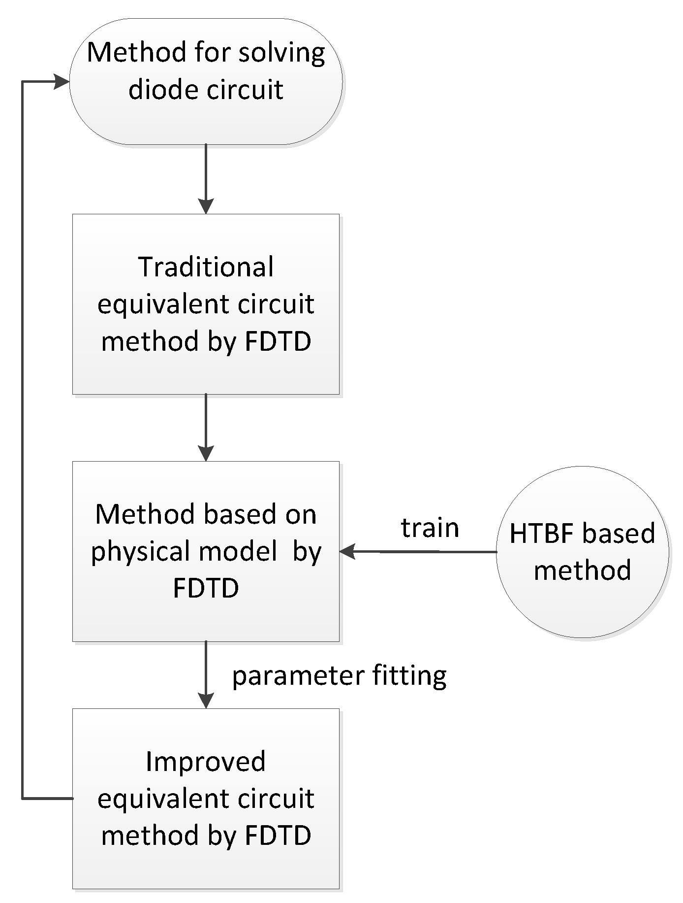
In view of the advantages and disadvantages of the above two methods, a new method of semiconductor device simulation based on a neural network is proposed in this paper. It is commonly known that since the rapid development of computer science, neural networks have been widely applied in engineering [9,10,11,12,13,14,15]. Underlying mapping features are extracted from training data of the same patterns to predict new outputs. Artificial neural networks have been used successfully in electromagnetic computation [16,17], such as in the hyperbolic tangent basis function neural model (HTBF), which replaces traditional PML, thus greatly reducing the calculation time of FDTD [18]. Based on the HTBF model, this study trains the diode model from the results achieved with the physical model method then, the HTBF-based model is used to extract the voltage–current equation of the diode through parameter fitting. The extracted voltage–current equation is applied to improve the traditional empirical formula in the equivalent circuit method. To the best of our knowledge, this simulation method of the diode circuit has not yet been reported.
This paper is organized as follows. The novel simulation method of the diode circuit is introduced in Section 2, along with the equivalent circuit method and the physical model method. In Section 3, the simulation results demonstrate the accuracy and efficiency of the proposed method. Finally, a conclusion is drawn in Section 4.
2. Theory and Formula
This section introduces the three methods mentioned above, explaining how to solve the equivalent circuit model as well as the physical model of the diode by FDTD, before describing the training method of the neural network model. Following this, a flow chart is provided to demonstrate the proposed method.
2.1. Equivalent Circuit Method
In the numerical simulation of antenna and microwave devices, nonlinear devices such as diodes and triodes are often included. The current passing through these circuit elements can be expressed as an impressed current density Ji, which is added to Maxwell’s equations:
where H and E represent magnetic and electric fields, respectively; is the dielectric constant; and is the conductivity. The impressed current is often used to represent a source or an unknown quantity. From a computational point of view, it is the source that generates the electric and magnetic fields, with a lumped element placed between two nodes whose characteristics are determined by the voltage and current flowing through them. This relation is incorporated into Maxwell’s equations through the voltage and electric field:
with the relationship between current and current density calculated via:
where S is the cross-sectional area of the cell grid, whose vector is parallel to current I.
As shown in Figure 1, the diode is located between the nodes (i, j, k) and (i, j, k + 1). The current direction follows the z direction, and Id can be described using the following formula:
where q is the absolute value of electron charge, k is the Boltzmann constant, and T is the thermodynamic temperature.
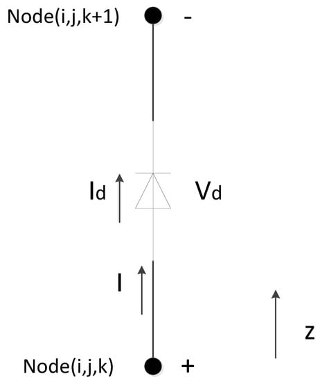
Figure 1.
Schematic diagram of the diode.
After differential treatment, the updating formula can be obtained:
where is the time step; is the electric field at the previous time step; and are the magnetic fields at the current time step; and are the space steps in the directions of x and y, respectively; is the dielectric constant in the direction of z; and is the conductivity in the direction of z. The Newton–Raphson method is used to solve the diode in Equation (5).
2.2. Method Based on the Physical Model
The basic equations of semiconductor devices consist of three parts: a carrier transport equation, a continuity equation, and the Poisson equation, which are summarized below into a set of basic differential equations for semiconductor device analysis:
where , Jn, , Jp, n, p, Na, q, Nd, G, t, and U are the permittivity, electron current density, electrostatic potential, hole current density, electron concentrations, hole concentrations, hole doping concentrations, electronic charge, electron doping concentrations, carrier generation rate, time, and recombination rate, respectively. Dp and Dn are the hole diffusion coefficient and the electron diffusion coefficient, respectively.
Taking p, n, and as a set of basic variables, the matrix formula is obtained after differential treatment:
where A, B, and C are the 3 × 3 coefficient matrix and F is the 3 × 1 dimensional constant matrix.
2.3. HTBF Based Method
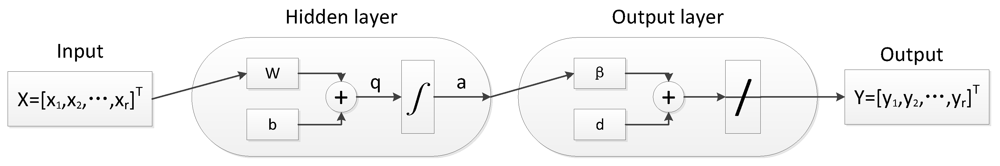
HTBF is widely used in artificial neural networks, especially in relation to fitting problems, where it can provide accurate predictions. The mapping function F of HTBF is shown in Figure 2.
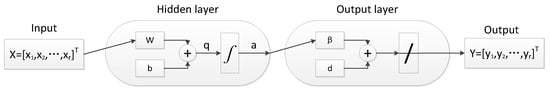
Figure 2.
Single hidden layer of an HTBF neural network.
Theoretically, a feedforward ANN with a single hidden layer can map any nonlinear transformation, where the input vector is connected to the output layer through the hidden layer. For hidden neurons in layer j, the input is , is the weight vector, bj is the scalar bias, and the transfer function F is the tan–sigmoid function:
The output a = [a1, a2, …, aS]T of the hidden layer constitutes the input vector of the output layer. Since the transfer function of the output layer is a linear function, the final output vector y can be expressed as:
where is the weight vector of the k-th output and is the scalar bias.
In this paper, the Levenberg–Marquardt algorithm with a lower mean square error is selected as the training algorithm. Firstly, the simulation results based on the traditional equivalent circuit are given, then the simulation results based on the physical model are provided. The simulation results based on the physical model are then trained with the HTBF neural network, and the voltage–current equation given by parameter fitting. Finally, the voltage–current equation is used to improve the empirical formula of the traditional equivalent circuit so that it can better reflect the working characteristics of the diode circuit under the conditions of large injection and high frequency. The flow chart is given in Figure 3 as follows.

Figure 3.
Flow chart of the HTBF base method.
3. Results
The advantages and disadvantages of the equivalent circuit method and the physical model method are described using several numerical examples, and the comprehensiveness, accuracy, and efficiency of the proposed method are proved by numerical experiments.
3.1. Equivalent Circuit Method
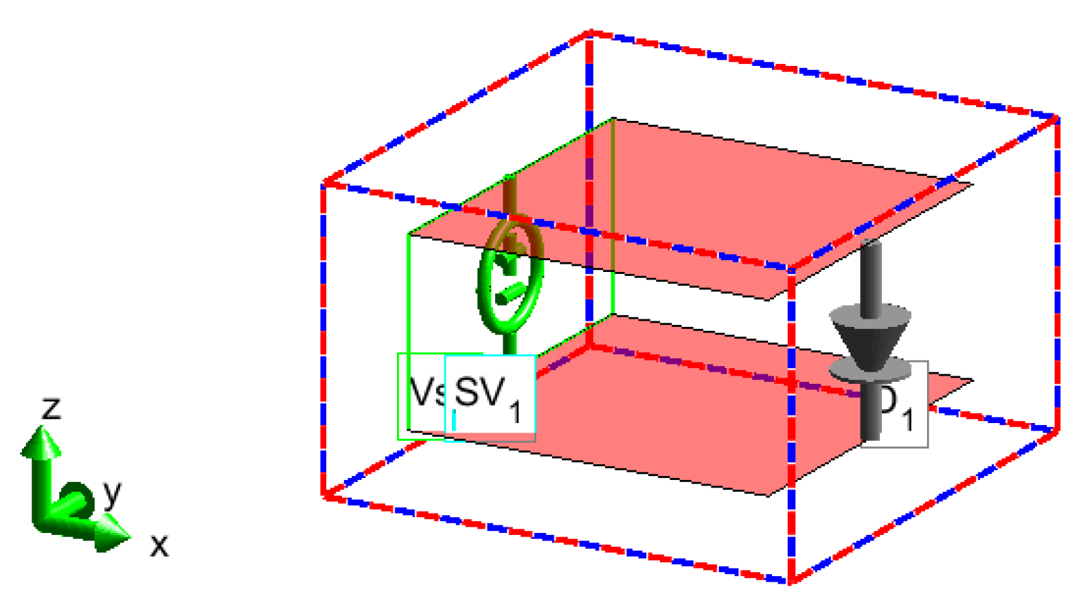
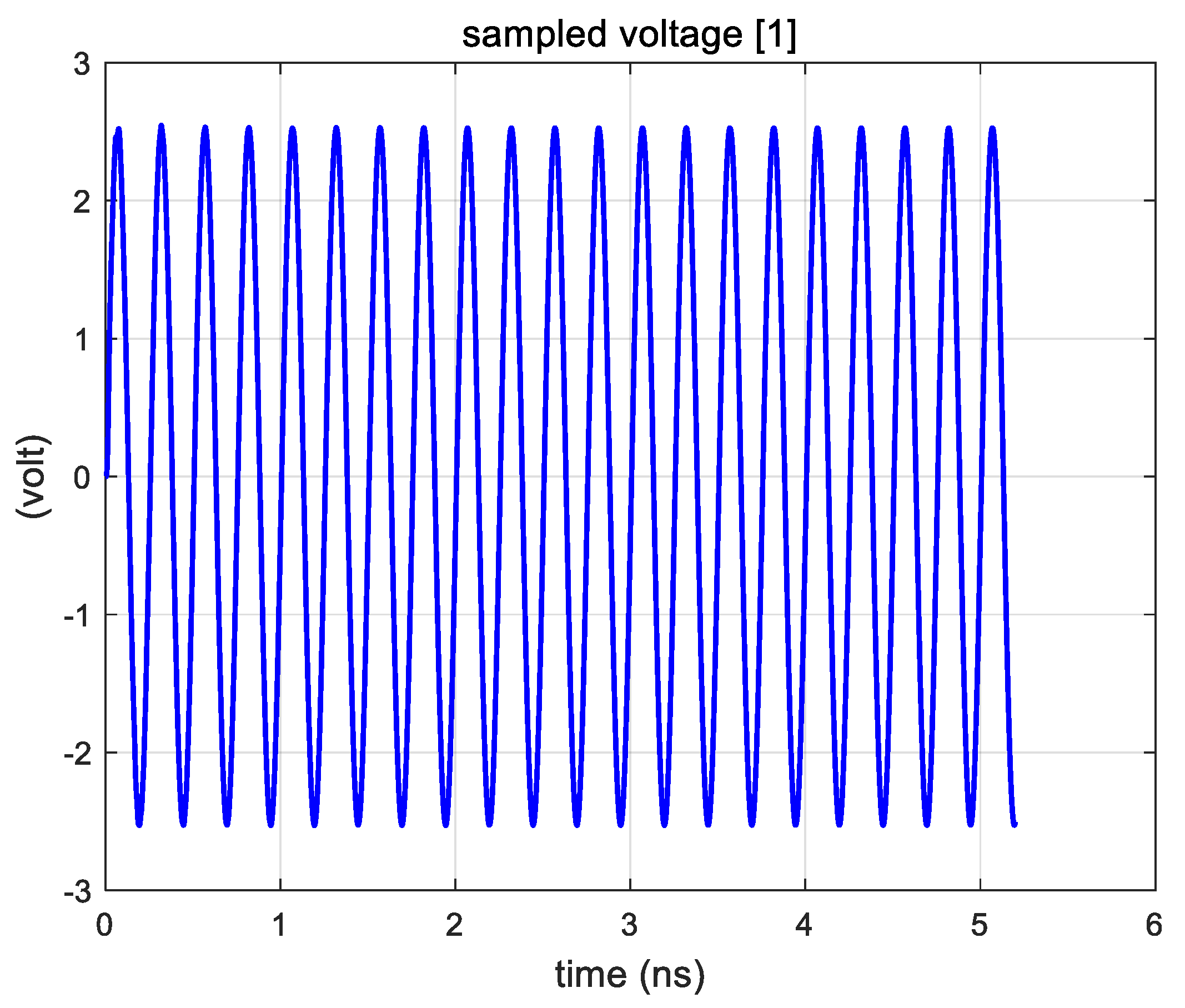
For the first example, consider a diode excited by a sine wave voltage source. Figure 4 shows the geometry of the problem. Two PEC parallel plates are defined as 1 mm apart. Between the two parallel plates, a voltage source with an external resistance of 50 is placed at one end and a diode pointing in the negative direction of z is connected at the other end. The signal is a sine wave with a frequency of 500 MHz and an amplitude of 10 V, and the sampling voltage is defined at both ends of the diode.
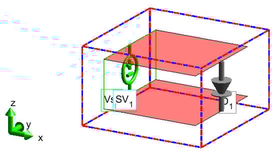
Figure 4.
Voltage source with terminal diode.
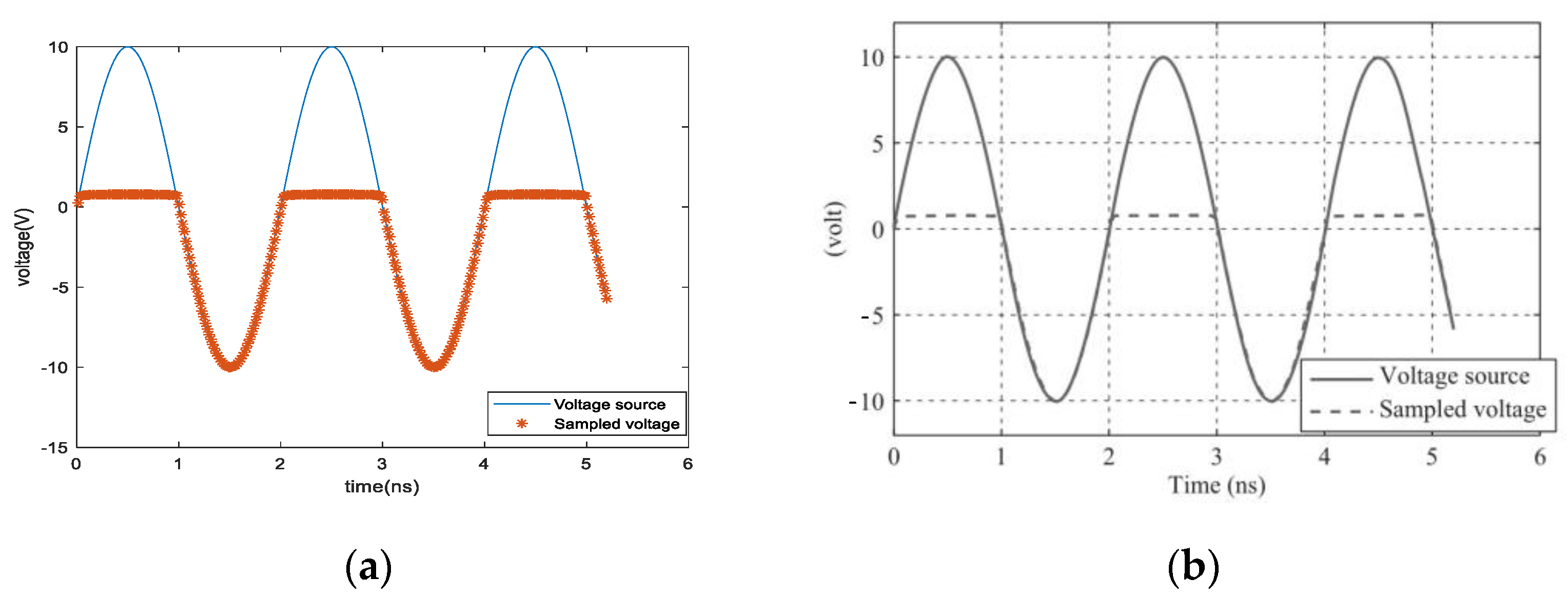
The simulation results are shown in Figure 5. The sampling voltage waveform confirms the response of the diode. When the source voltage is higher than 0.7 V, the diode’s sampling voltage remains 0.7 V, which is consistent with the theoretical analysis and can be compared with the results in the reference [19].
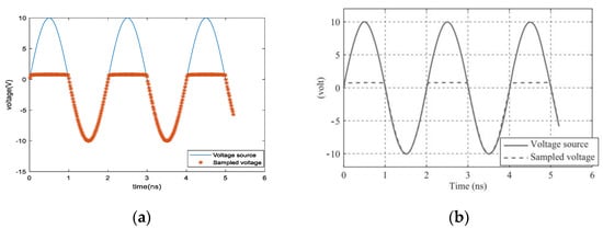
Figure 5.
Excitation source waveform and sampling voltage waveform: (a) simulation result; (b) reference result.
3.2. Method Based on the Physical Model
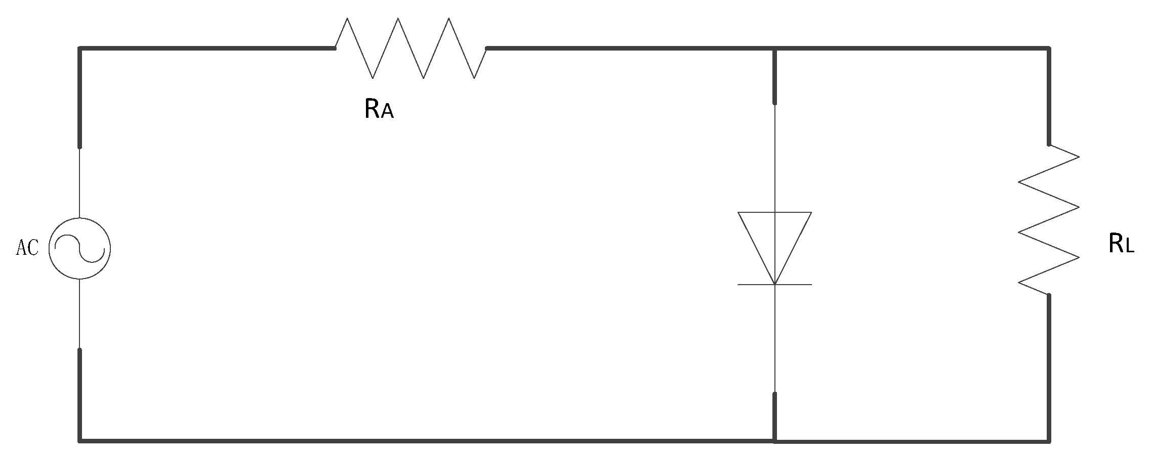
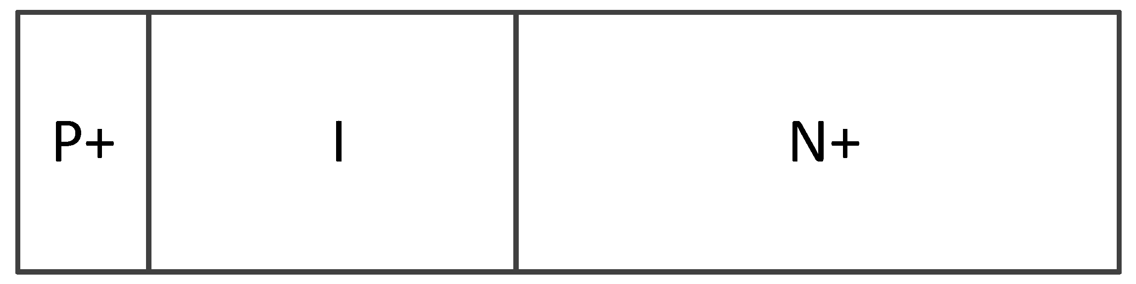
The second example analyzes the limiter circuit composed of a PIN diode, as shown in Figure 6. RA and RL are the equivalent resistance and load impedance, both set to 50 . The PIN diode takes a one-dimensional model, as shown in Figure 7.
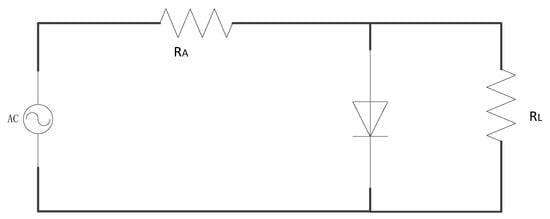
Figure 6.
Shunt diode limiter circuit.

Figure 7.
One-dimensional physical model of the PIN diode.
The material of the PIN diode is silicon, the thickness of the center I region is 4 um and the doping concentration is 1015 cm−3. The thickness of the p-region is 1 um, and the surface concentration of the p-type diffusion layer is 1019 cm−3. The thickness of the n-region is 7 um and the surface concentration of the diffusion layer in the n-region is 1019 cm−3. The cross-sectional area of the conduction region of the PIN diode is 10−5 cm−2.
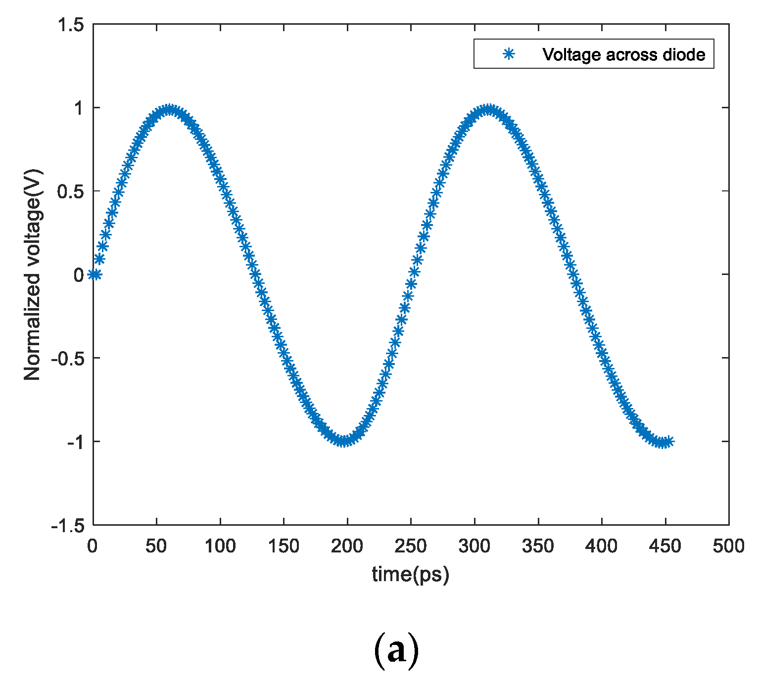
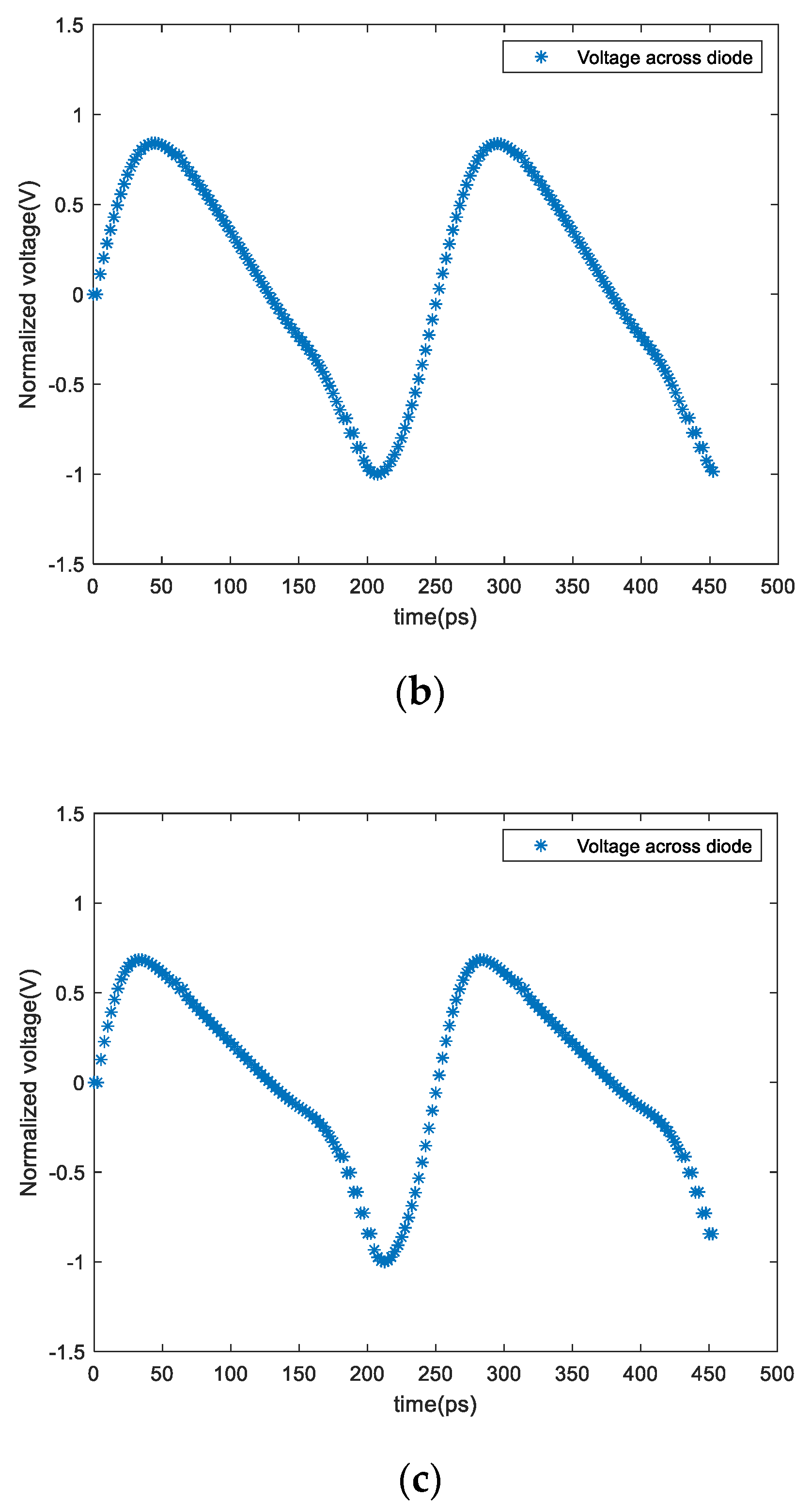
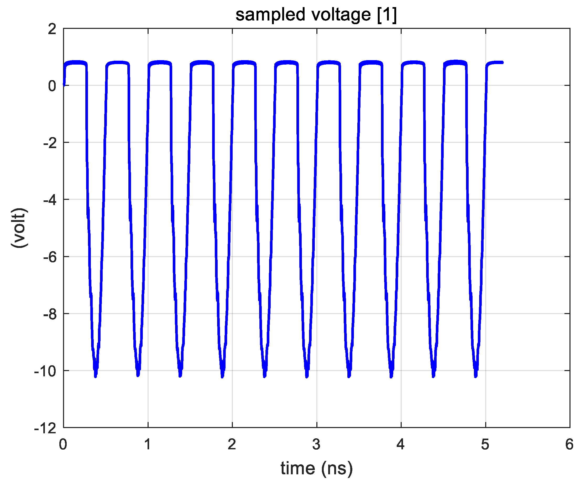
The voltage applied to the circuit power supply is a sine wave with a frequency of 4.0 GHz, and the voltage amplitude Vm is 5 V, 50 V, and 100 V, respectively. The voltage at both ends of the diode is obtained, as shown in Figure 8. The calculation results are normalized (voltage is normalized by the negative peak voltage in the first cycle). Ideally, PIN diodes exhibit a high impedance at a low input power (equivalent to low input voltage) and a low impedance at a high voltage, thus cutting out the load and protecting it.
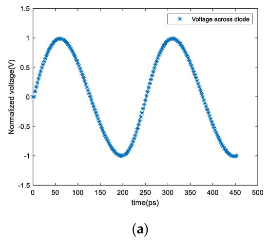
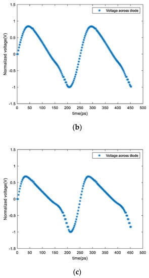
Figure 8.
Diode voltage obtained with different amplitudes: (a) amplitude of 5 V; (b) amplitude of 50 V; (c) amplitude of 100 V.
As can be seen from Figure 8a–c, when Vm = 5 V, the voltage at both ends of the PIN diode is approximately sinusoidal. When Vm = 50 V, the forward voltage and reverse voltage of the PIN diode are asymmetric, showing nonlinear, large signal characteristics. When the high voltage Vm = 100 V, the voltage asymmetry at both ends of the PIN diode is more significant. This is consistent with the conclusion in the reference [20].
3.3. HTBF Based Method
In this section, the HTBF based method described above is divided into two parts. Firstly, the results obtained by the physical model method are trained by the HTBF neural network to speed up its simulation efficiency. Secondly, the HTBF based diode model is used to extract the voltage–current equation of the diode through parameter fitting. Then, the extracted voltage–current equation is applied to improve the traditional empirical formula in the equivalent circuit method and solved by FDTD again. The results show that the improved equivalent circuit method can better reflect the diode electrical characteristics under large injection conditions and high frequency.
3.3.1. HTBF Model Method
The diode parameters and circuit selection in this method are consistent with those used in Section 3.2. In this example, to train the HTBF model, 37 groups of data were obtained using the physical model method and are used as the data set. The simulation time of the results based on the physical model method was over 4 h. We randomly selected 90% to be used as training data, 5% for validation, and the remaining 5% for the testing data set. Our model is benchmarked in MATLAB 2018b with the deep learning toolbox [21]. The training process took approximately 20 min and the relative error during the training process was as follows.
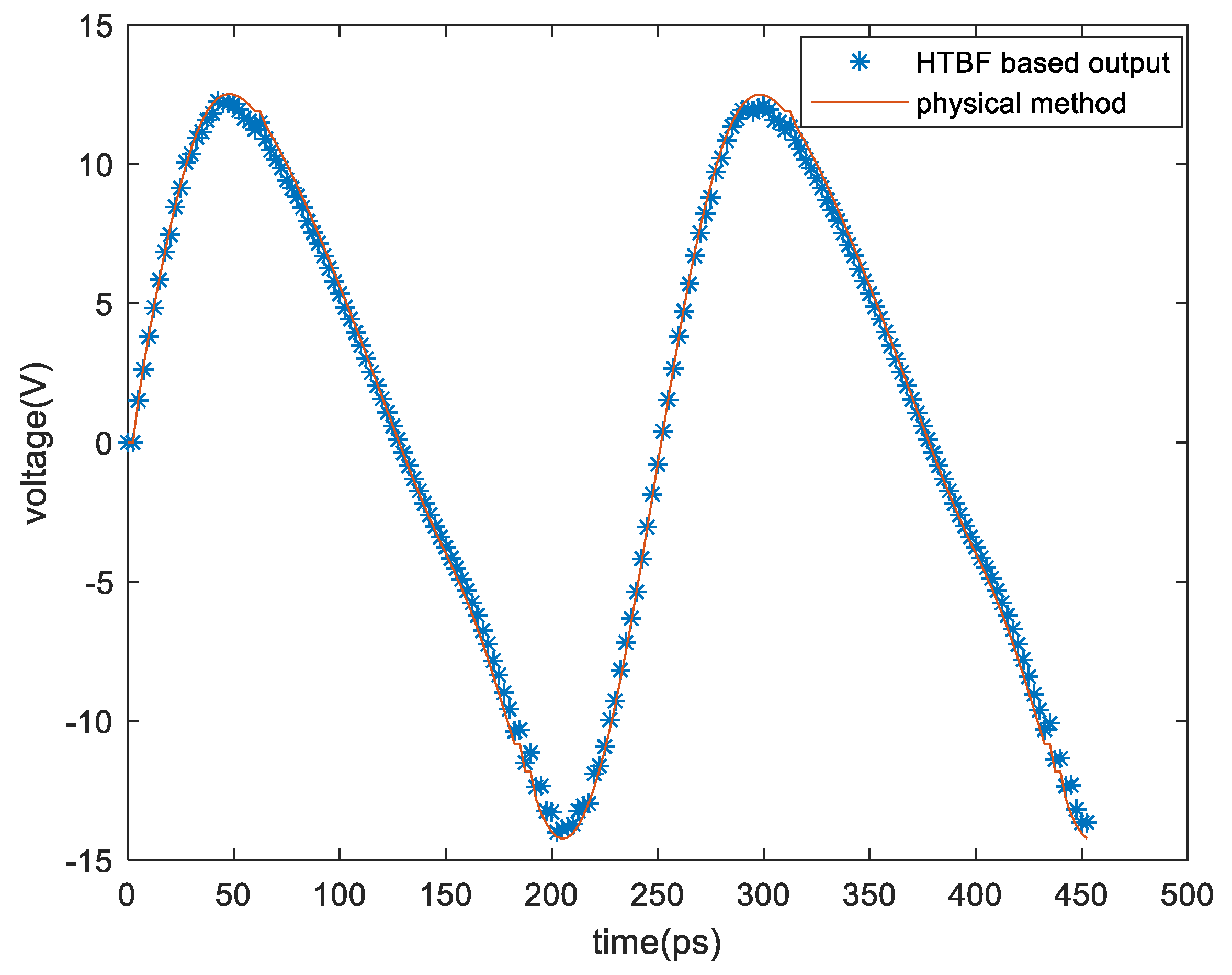
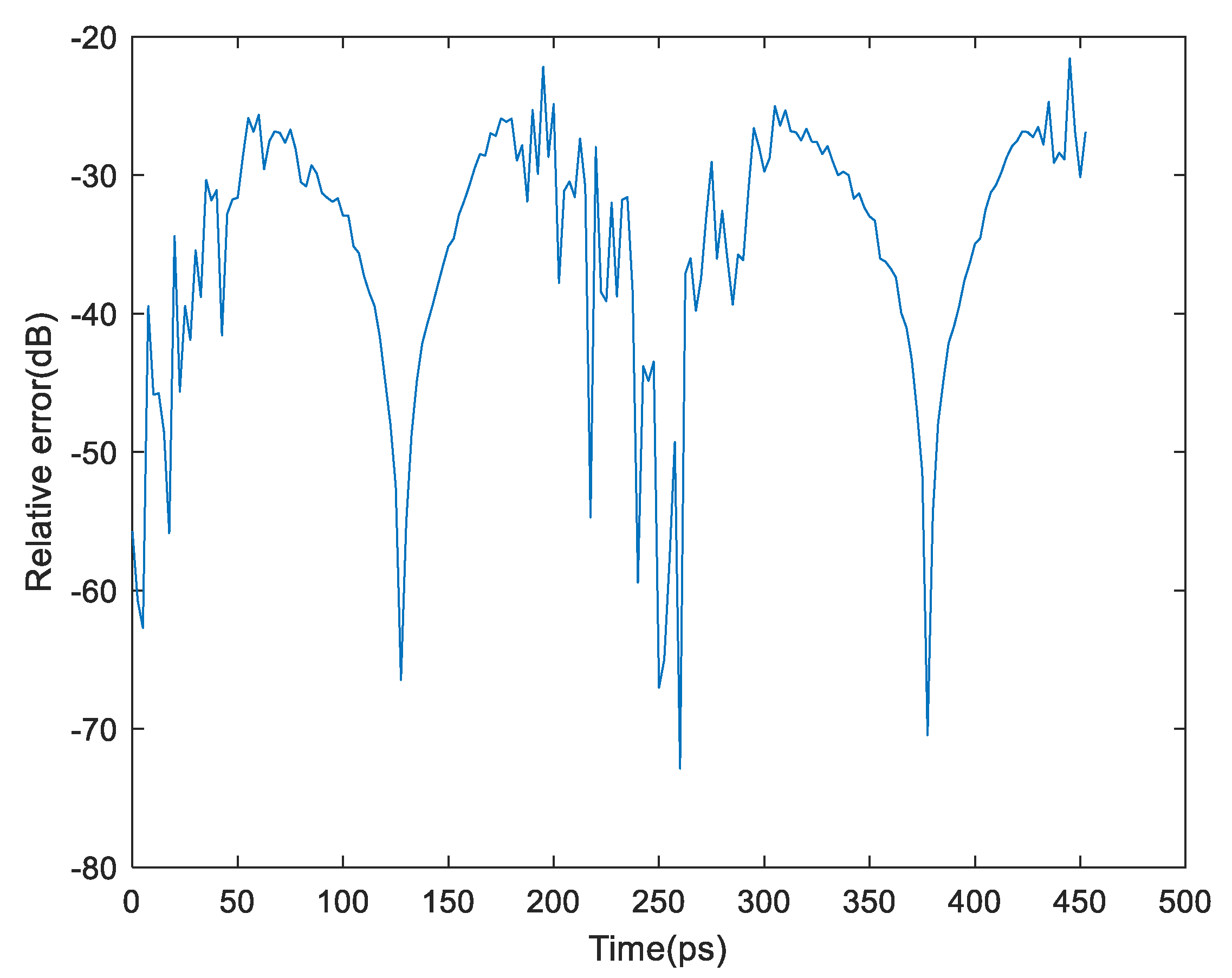
The HTBF model was used to predict the voltage at both ends of the diode. Changing the voltage source amplitude to 40V, as shown in Figure 9, proved that the results of the diode model based on HTBF was consistent with the calculation results of the physical model method. The relative error is defined as:
where v_HTBF is the voltage of the HTBF based output, v_physical is the physical method output, and v_physicalmax is the maximum value of the voltage across the diode which is based on the physical method. We present the average error in Figure 10. As can be seen, the average error is below −20 dB, therefore the HTBF method is reliable.
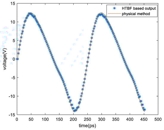
Figure 9.
Comparison between the PIN diode voltage calculated by the HTBF method and the physical model method.
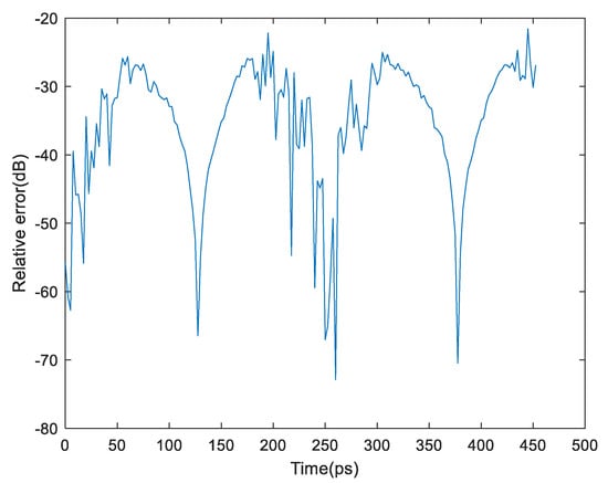
Figure 10.
Relative error between the HTBF method and the physical model method.
Comparing the simulation time of the physical model method and the HTBF method, as shown in Table 1, it is found that the simulation time of the HTBF method is significantly faster than the physical model method under the same conditions.

Table 1.
Comparison between the physical model method and the HTBF method.
3.3.2. Improved Equivalent Circuit Method
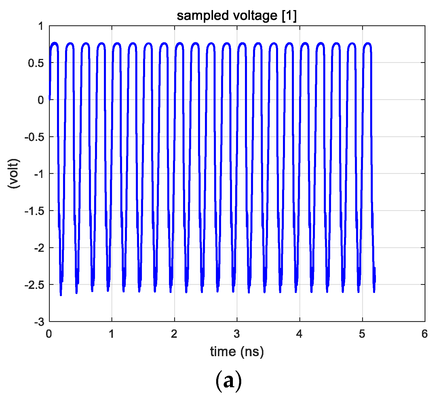
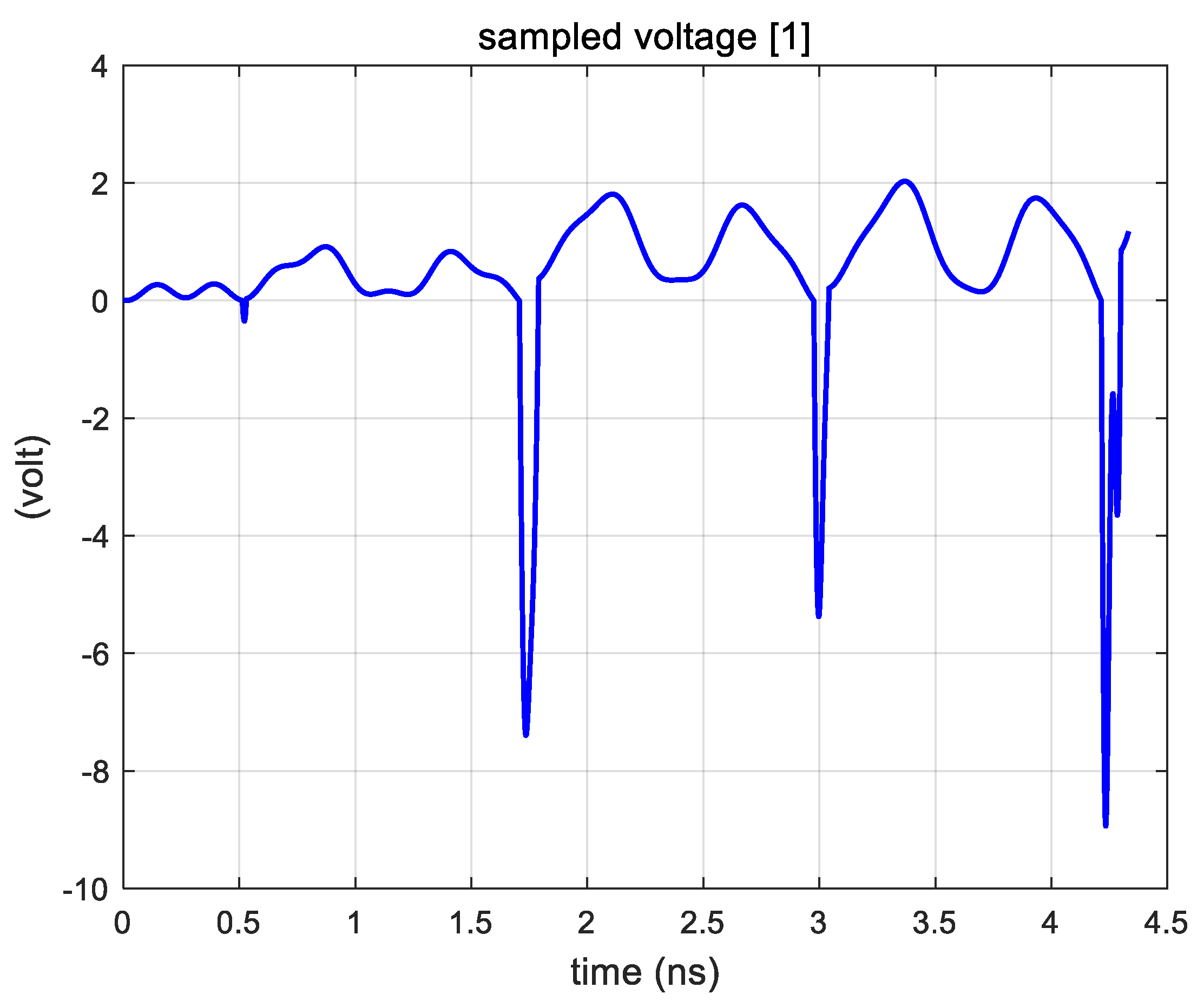
According to the above HTBF method based on the physical model, it can be observed that the traditional equivalent circuit method cannot simulate well under the conditions of high frequency and large injection. The circuit shown in Figure 6 is solved by the traditional equivalent circuit method, and the amplitude of the excitation source is set to 5 V, 10 V, and 20 V, respectively, to obtain the results shown in Figure 11. The frequency of the source is 4 GHz as it is in Section 3.2.
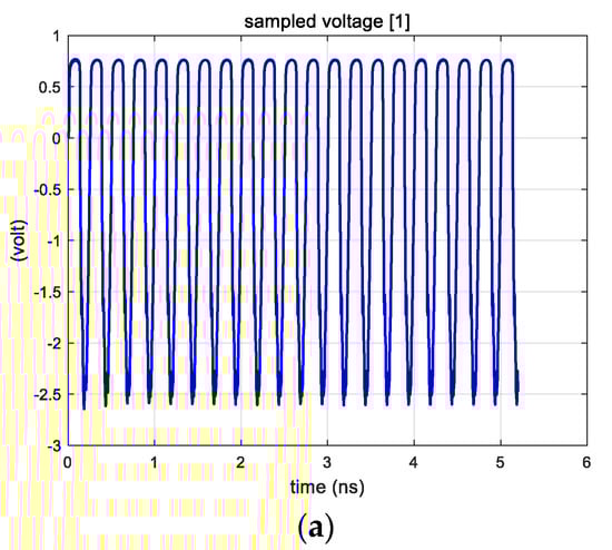
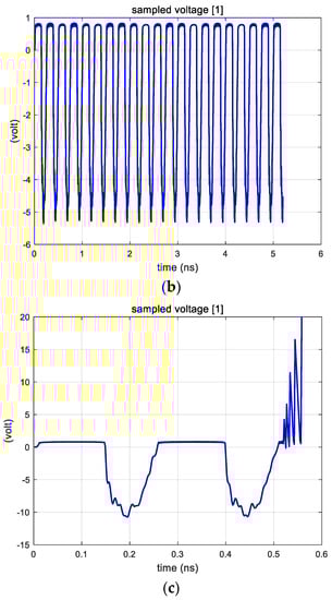
Figure 11.
Sampled voltage across the diode using the traditional equivalent circuit method: (a) amplitude of 5 V; (b) amplitude of 10 V; (c) amplitude of 20 V.
As can be observed in Figure 11a–c, when the amplitude of the source changes from 5 V to 20 V, the results obtained by the traditional equivalent circuit method gradually tend to become unstable and diverge at 20 V. Therefore, compared with Figure 8a–c, it can be concluded that the traditional equivalent circuit formula cannot correctly reflect the diode circuit characteristics at high frequency, and fails when excited by high power (equivalent to high input voltage).
In the following example, based on the physical model method accelerated by HTBF, we fit the empirical formula to improve the traditional equivalent circuit formula, so that the improved equivalent circuit formula can also be applied in the conditions of high frequency and high power. Here we adopted the curve fitting tool in Matlab 2018, and the improved voltage–current equation is listed as follows:
where , , , and are control coefficients; V0 is the empirical voltage value; f0 is the empirical value; f represents the frequency of solving the problem; represents the step function; L0 is the empirical inductance value; C1 and C2 are empirical value, V1 represents the startup voltage of diode.
The physical meaning of the formula is defined as follows. When the frequency f is lower than f0, it is calculated according to the traditional empirical formula. When f is higher than f0, the traditional empirical formula is no longer applicable. At ahigh frequency and low voltage, the diode presents high impedance characteristics, and at a high frequency and high voltage, the diode presents low impedance characteristics. and are used, respectively, to control the diode response to low power input (equivalent to low input voltage) and high power input (equivalent to high input voltage), at high frequency.
The simulation of the circuit shown in Figure 6 was then repeated using the improved equivalent circuit formula with f0 = 2 GHz, V0 = 10 V, L0 = 6 H, a = 2, b = 2, C1 = 100 pF, C2 = 1 pF, V1 = 0.7 V. Three provided examples verify the effectiveness of the improved equivalent circuit method:
- A.
- f = 400 MHz, Vm = 20 V
In the first example, we defined the frequency for solving the problem as 400 MHz and the maximum amplitude of the excitation source as 20 V. It is used for testing the improved equivalent circuit formula at low frequency. The results are shown in Figure 12.
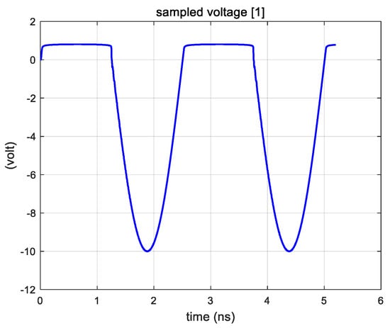
Figure 12.
Results for the improved equivalent circuit method.
As can be observed, these results are consistent with the traditional equivalent circuit method.
- B.
- f = 4 GHz, Vm = 5 V
In the second example, we defined the frequency for solving the problem as 4 GHz and the maximum amplitude of the excitation source as 5 V. It is used for testing the improved equivalent circuit formula at high frequency and low voltage injection. The results are shown in Figure 13.
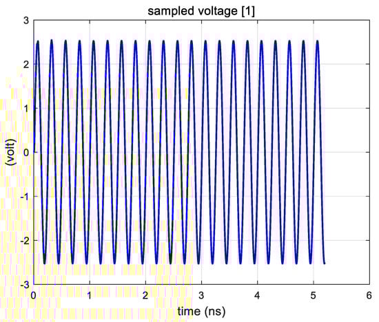
Figure 13.
Results for the improved equivalent circuit method.
Compared with Figure 8a, the improved equivalent circuit method has feedback characteristics similar to the physical model at high frequency and low voltage injection.
- C.
- f = 4 GHz, Vm = 20 V
In the third example, we defined the frequency for solving the problem as 4 GHz and the maximum amplitude of the excitation source as 20 V. It is used for testing the improved equivalent circuit formula at high frequency and high voltage injection. In order to facilitate comparison, the results of the same excitation amplitude at 2 GHz are given by using the traditional equivalent circuit method. The results are shown in Figure 14.
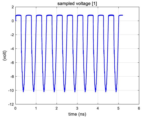
Figure 14.
Results for the traditional equivalent circuit method.
Now we give the simulation results obtained by using the improved equivalent circuit formula when the amplitude of the excitation source is 20 V at 4 GHz. As can be observed in Figure 15, the improved equivalent circuit method can work at a high frequency and high power.
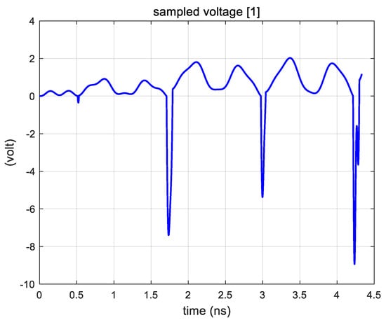
Figure 15.
Results for the improved equivalent circuit method.
4. Conclusions
In this paper, a novel simulation method based on a HTBF neural network was proposed based on the existing analysis methods for diode electrical characteristics. The traditional equivalent circuit analysis method is widely used, but it cannot reflect the transient response of the device in the case of large injection. Moreover, it becomes invalid at high frequency. The field-circuit co-simulation analysis method based on the physical model better reflects the physical mechanism, but its simulation efficiency is low, so the HTBF method was used to accelerate the simulation. The improved voltage–current equation was extracted through parameter fitting, and then, the improved equivalent circuit method, based on the new voltage–current equation, was solved by FDTD. The results show that the improved equivalent circuit method can reflect the working state of the diode circuit under a large injection and high frequency better than the traditional equivalent circuit method.
Author Contributions
Conceptualization, L.X.; methodology, T.L. and Y.Y.; software, H.W.; validation, T.L.; formal analysis, N.W.; investigation, T.L.; resources, L.X.; data curation, Y.H.; writing—original draft preparation, T.L.; writing—review and editing, X.Y. and F.W.; visualization, Y.H.; supervision, X.S. All authors have read and agreed to the published version of the manuscript.
Funding
This research received no external funding.
Conflicts of Interest
The authors declare no conflict of interest.
References
- Hirakawa, T.; Hao, Z.; Shinohara, N.; Guo, Y.X. The method of diode modeling and novel equivalent circuit for microwave rectifiers. In Proceedings of the 2019 IEEE Asia-Pacific Microwave Conference (APMC), Singapore, 10–13 December 2019; pp. 991–993. [Google Scholar] [CrossRef]
- Pendharkar, S.P.; Winterhalter, C.R.; Shenai, K. A Behavioral Circuit Simulation Model for High-Power GaAs Schottky Diodes. IEEE Trans. Electron. Devices 1995, 42, 1847–1854. [Google Scholar] [CrossRef]
- Liu, C.; Tan, F.; Zhang, H.; He, Q. A Novel Single-Diode Microwave Rectifier with a Series Band-Stop Structure. IEEE Trans. Microw. Theory Tech. 2017, 65, 600–606. [Google Scholar] [CrossRef]
- Chen, X.; Chen, J.; Huang, K.; Xu, X. A Circuit Simulation Method Based on Physical Approach for the Analysis of Mot_bal99lt1 p-i-n Diode Circuits. IEEE Trans. Electron. Devices 2011, 58, 2862–2870. [Google Scholar] [CrossRef]
- Chen, J.; Chen, X.; Liu, C.; Huang, K.; Xu, X. Analysis of Temperature Effect on P-I-N Diode Circuits by a Multiphysics and Circuit Cosimulation Algorithm. IEEE Trans. Electron. 2012, 59, 3069–3077. [Google Scholar] [CrossRef]
- Zeng, H.; Tang, Y.; Duan, X.; Chen, X. A Physical Model-Based FDTD Field-Circuit Co-Simulation Method for Schottky Diode Rectifiers. IEEE Access 2019, 7, 87265–87272. [Google Scholar] [CrossRef]
- Hongzheng, Z.; Ke, X.; Xing, C. Analysis of Schottky diode detector circuit based on multiphysics simulation. In Proceedings of the 2018 International Conference on Microwave and Millimeter Wave Technology (ICMMT), Chengdu, China, 7–11 May 2018; pp. 1–3. [Google Scholar] [CrossRef]
- Chen, S.; Ding, D.; Yu, M.; Wang, Y.; Chen, R. Electro-Thermal Analysis of Microwave Limiter Based on the Time-Domain Impulse Response Method Combined with Physical-Model-Based Semiconductor Solver. IEEE Trans. Microw. Theory Tech. 2020, 68, 2579–2589. [Google Scholar] [CrossRef]
- Sorokosz, L.; Zieniutycz, W. Electromagnetic modeling of microstrip elements aided with artificial neural network. In Proceedings of the Baltic URSI Symposium (URSI), Warsaw, Poland, 5–8 October 2020; pp. 85–88. [Google Scholar] [CrossRef]
- Tian, F.; Yang, Y.; Mao, L. Electromagnetic inversion algorithm based on convolutional neural network. In Proceedings of the Cross Strait Radio Science & Wireless Technology Conference (CSRSWTC), Fuzhou, China, 13–16 December 2020; pp. 1–3. [Google Scholar] [CrossRef]
- Xiong, J.; Chen, Z.; Xiu, Y.; Mu, Z.; Raginsky, M.; Rosenbaum, E. Enhanced IC modeling methodology for system-level ESD simulation. In Proceedings of the 40th Electrical Overstress/Electrostatic Discharge Symposium (EOS/ESD), Reno, NV, USA, 23–28 September 2018; pp. 1–10. [Google Scholar] [CrossRef]
- Liang, W.; Yang, X.; Loiseau, A.; Mitra, S.; Gauthier, R. Novel ESD compact modeling methodology using machine learning techniques. In Proceedings of the 42nd Annual EOS/ESD Symposium (EOS/ESD), Reno, NV, USA, 13–18 September 2020; pp. 1–7. [Google Scholar]
- Yao, H.M.; Sha, W.E.I.; Jiang, L. Two-Step Enhanced Deep Learning Approach for Electromagnetic Inverse Scattering Problems. IEEE Antennas Wirel. Propag. Lett. 2019, 18, 2254–2258. [Google Scholar] [CrossRef]
- Li, L.; Wang, L.G.; Teixeira, F.L. Performance Analysis and Dynamic Evolution of Deep Convolutional Neural Network for Electromagnetic Inverse Scattering. IEEE Antennas Wirel. Propag. Lett. 2019, 18, 2259–2263. [Google Scholar] [CrossRef]
- Jin, H.; Ma, H.; Butala, M.D.; Liu, E.; Li, E. EMI Radiation Prediction and Structure Optimization of Packages by Deep Learning. IEEE Access 2019, 7, 93772–93780. [Google Scholar] [CrossRef]
- Yao, H.M.; Jiang, L.J. Machine learning based neural network solving methods for the FDTD method. In Proceedings of the IEEE International Symposium on Antennas and Propagation & USNC/URSI National Radio Science Meeting, Boston, MA, USA, 8–13 July 2018; pp. 2321–2322. [Google Scholar] [CrossRef]
- Zhang, H.H.; Jiang, L.J.; Yao, H.M. Embedding the Behavior Macromodel into TDIE for Transient Field-Circuit Simulations. IEEE Trans. Antennas Propag. 2016, 64, 3233–3238. [Google Scholar] [CrossRef]
- Yao, H.M.; Jiang, L. Machine-Learning-Based PML for the FDTD Method. IEEE Antennas Wirel. Propag. Lett. 2019, 18, 192–196. [Google Scholar] [CrossRef]
- Elsherbeni, A.; Demir, V. The Finite Difference Time Domain Method for Electromagnetics: With MATLAB Simulations [M]; SciTech Publishing: New York, NY, USA, 2016. [Google Scholar]
- Mamoru, K. Numerical Analysis of Semiconductor Devices [M]; Electronic Industry Press: Beijing, China, 1985. [Google Scholar]
- Kim, P. MATLAB Deep Learning [M]; Apress: New York, NY, USA, 2017. [Google Scholar]

Publisher’s Note: MDPI stays neutral with regard to jurisdictional claims in published maps and institutional affiliations. |
© 2021 by the authors. Licensee MDPI, Basel, Switzerland. This article is an open access article distributed under the terms and conditions of the Creative Commons Attribution (CC BY) license (https://creativecommons.org/licenses/by/4.0/).