Article

A Systematic Assessment of W-Doped CoFeB Single Free Layers for Low Power STT-MRAM Applications

IMEC, Kapeldreef 75, 3001 Leuven, Belgium
*
Author to whom correspondence should be addressed.
Electronics 2021, 10(19), 2384; https://doi.org/10.3390/electronics10192384
Submission received: 9 August 2021 / Revised: 17 September 2021 / Accepted: 18 September 2021 / Published: 29 September 2021
(This article belongs to the Special Issue High-Density Solid-State Memory Devices and Technologies)

Abstract

:
Spin-transfer torque magnetoresistive random access memory (STT-MRAM) technology is considered to be the most promising nonvolatile memory (NVM) solution for high-speed and low power applications. Dual MgO-based composite free layers (FL) have driven the development of STT-MRAMs over the past decade, achieving data retention of 10 years at the cost of higher write power consumption. In addition, the need for tunnel magnetoresistance (TMR)-based read schemes limits the flexibility in materials beyond the typical CoFeB/MgO interfaces. In this study, we propose a novel spacerless FL stack comprised of CoFeB alloyed with heavy metals such as tungsten (W) which allows effective modulation of the magnet properties (Ms, Hk) while retaining compatibility with MgO layers. The addition of W results favours a delayed crystallization process, in turn enabling higher thermal budgets up to 180 min at 400 °C. The presence of tungsten reduces the total FL magnetization (Ms) but simultaneously increasing its temperature dependence, thus, enabling a dynamic write current reduction of ~15% at 2 ns pulse widths. Reliable operation is demonstrated with a WER of 1 ppm and endurance >1010 cycles. These results pave the way for alternative designs of STT-MRAMs for low power electronics.

Graphical Abstract

1. Introduction

Recent advancements in the computing community such as cloud computing and the Internet-of-Things (IoT) have increasingly created a heavy demand for an on-board memory solution in terms of speed and reduced power consumption. To tackle this growing problem, researchers have investigated several nonvolatile memory (NVM) technologies. STT-MRAM technology is considered to be the most viable solution owing to its attractive properties such as CMOS process compatibility, high operation speeds, superior endurance, and negligible leakage, thus, making it an ideal solution for low power, embedded electronics [1,2,3]. Significant resources have been invested in the past decade at major foundries and tool suppliers to optimize this technology for last-level cache (LLC) memory, microcontroller units (MCU), eFLASH, and automotive applications [2,4,5,6,7,8,9,10,11,12]. Despite these excellent advancements, some challenges remain. Further reduction of the write power consumption is required to ensure product lifetimes and enable further scaling at advanced logic nodes. This outstanding challenge persists due to an apparent tradeoff between the required write current for an achievable data retention (or thermal stability) of the free (or storage) layer in STT-MRAM devices.
The switching dynamics of the free layer (FL) have been extensively explored and are well described by the Landau–Lifshitz–Gilbert–Slonczeweski (LLGS) equation. For perpendicular magnetic tunnel junctions (pMTJs), reasonable predictions for the write current can be made using the coherent reversal model [13,14]. Then, the write current (Ic) and the switching time (t) in the precessional switching regime can be expressed as:
I c I c o 1 = ln π / 2 θ o t / t o
I c o = 4 η 2 α e M s t π d 2 H k
where Ico refers to the critical write current at zero temperature and is purely dependent on material properties, θo is the initial angle between the magnetic moment and the easy axis of the magnetic anisotropy, and to is the characteristic relaxation time of the FL magnetization. Ms, Hk, α, and η correspond to the saturation magnetization, effective magnetic anisotropy field, damping, and spin polarization, respectively. The FL properties are described by the critical dimension (CD, d) and thickness (t). To improve write performance, optimization of one or more material parameters has been the conventional route. Given Δ = M s H k t d / 2 k B T , Equation (1) can be rewritten as:
I c 0 = 4 e k B T α η Δ
Thus, the tradeoff between write current and thermal stability (Δ) becomes the key limiter. In addition, tunnel magnetoresistance (TMR)-based read schemes require a high TMR for fast reading, and thus are limited to the interfacial CoFeB/MgO system, which in turn results in a limited scope for materials exploration. As a result, most efforts in write current reduction have focused on optimizing the conventional dual MgO-based composite FL stack with spacer and cap layer engineering [6,15,16,17,18,19].
Here, we propose an alternative route for write current reduction through alloying conventional STT-MRAM materials such as CoFeB with nonmagnetic metals such as tungsten (W). The key advantage of this method is that it enables a precise and continuous variation of the FL properties (Ms, Hk) and the overall MTJ crystallization temperature. In this study, we demonstrate improved STT-MRAM write performances with a novel FL design based on a single W-CoFeB alloyed layer. The addition of W enables precise control of the FL magnetization (Ms) and its temperature dependence, aiding a current reduction during the write process. As Ic0 and Δ are largely dependent on static magnetic properties of the FL (Ms, Hk), we find the coherent model of reversal, as described in Equations (1)–(3), a convenient and reasonably accurate model to elucidate the general performance trends for W-based alloyed FL designs as compared with conventional FLs. The introduction of metallic impurities or dopants in or near the FL has been explored recently, but this has been limited to enabling higher thermal budgets for compatibility of STT-MRAMs with Si-based backend-of-the-line (BEOL) processing [17,20]. Some device-level assessments of Δ have been carried out within the framework of spacer material optimization in conventional FLs; however, the lack of absolute metrics limits a fair evaluation of the true benefits of alloying CoFeB FLs with nonmagnetic dopants. Here, we systematically discuss the impact of heavy metal (such as W) doping from hypothesis and stack development to a full device-level assessment including write performance as low as a 1 ppm level, thermal stability, breakdown, and cycling. We demonstrate that this tuneable FL design opens up avenues for production-level development of STT-MRAMs, while maintaining application-relevant figures of merit.

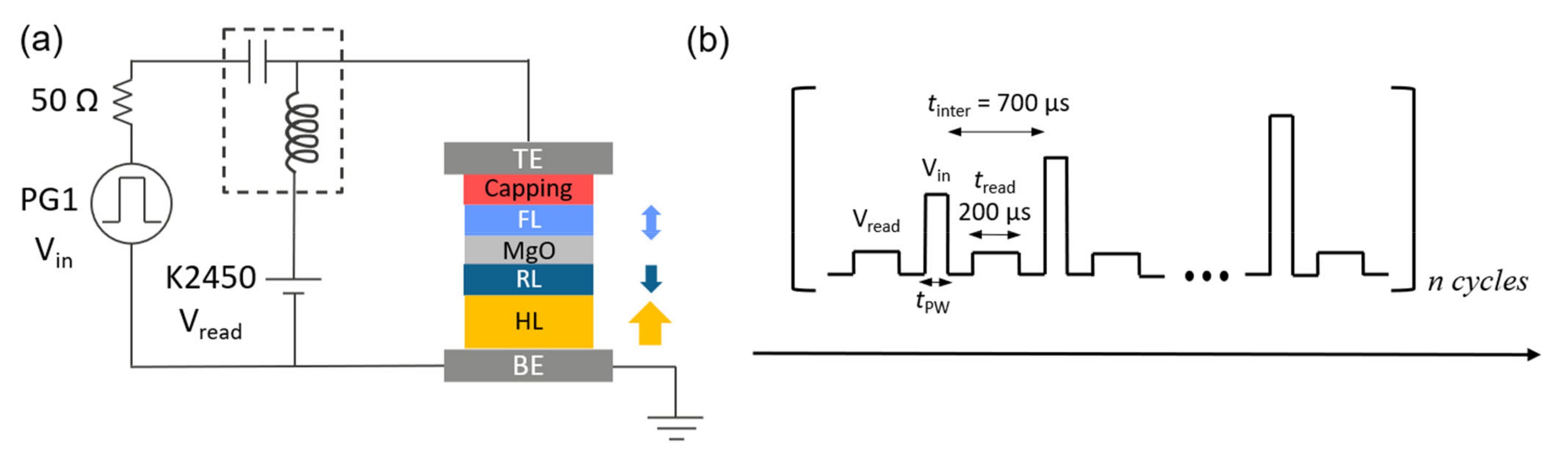
2. Materials and Methods

Bottom-pinned pMTJ stacks were deposited on thermally oxidized Si (001) wafers by magnetron sputtering in a Canon-ANELVA EC7800 cluster tool at IMEC’s state-of-the-art 300 mm assembly line. Two pMTJ stacks were deposited. The two stacks shared the same hard layer (HL) and reference layer (RL) composition, while the free layer (FL) composition was varied. One stack comprised the conventional composite FL CoFeB/Ta/CoFeB (t = 2.5 nm with a 3 Å-thick Ta spacer layer) and served as the reference stack for this study. The second stack comprised the proposed new FL WxCoFeB1-x (t = ~3 nm). The compositional variation of the new FL was achieved by varying the deposition power of the W and composite Co46.7Fe23.3B30 targets. The hard layer (HL) was a [Co/Pt]x-based multilayer, and the reference layer was a [Co/spacer/FeB]-based trilayer stack. The HL and RL were coupled through a metallic spacer to form a synthetic antiferromagnet (SAF). A 1 nm thick MgO tunnel barrier was retained for both stacks. The reference stack was annealed at 400 °C for 30 min, while the W-based stack was annealed at 400 °C for 180 min. Patterned MTJ devices of critical dimension CD (or d) = 50 nm were fabricated by 193 nm immersion lithography, and a modified ion beam etch process [11] that suppressed etch-induced MTJ damage. All samples were subjected to a 2 T magnetic field at the end-of-line (EOL) to orient the SAF magnetization direction.
Vibrating sample magnetometry (VSM) was used at the film level to measure the out-of-plane magnetization (Mz) as a function of magnetic field and temperature. For device-level characterization, we used a Hprobe MRAM prober equipped with a Keysight M8190A pulse generator (trise = 70 ps, τ P W ,   m i n = 200 ps), a Keithley 2450 source and measurement unit (SMU), and digital multimeter (DMM). The interval time between the read and write pulses was optimized to 700 µs, while the read pulse duration was fixed at 200 µs. A write-verify scheme was adopted for both the write performance and WER studies, while for the endurance measurement, MTJ resistance reads were limited to five read sequences per decade of cycling events. Positive voltage bias (VMTJ > 0) resulted in AP-to-P switching, while negative bias (VMTJ < 0) resulted in P-to-AP switching.
The breakdown statistics were collected by electrically stressing the MTJ devices with a ramped step function voltage waveform, as described previously [21,22].

3. Results and Discussion

In this section, we evaluate the device-level performance of the WxCoFeB(1-x) alloy as a free layer for STT-MRAM devices in the context of low power applications. The results and discussion are presented in a three-fold manner: First, the fundamental MTJ properties are assessed and the role of W in enabling extended BEOL compatibility is discussed; in the second subsection, we investigate the writing performance by quasi-static switching experiments as low as 2 ns current pulses, and the impact of W doping on anomalous behaviour such as backhopping; finally, the device reliability is assessed by means of breakdown trends, data retention, write error rates, and lifetime extrapolations at operating conditions.

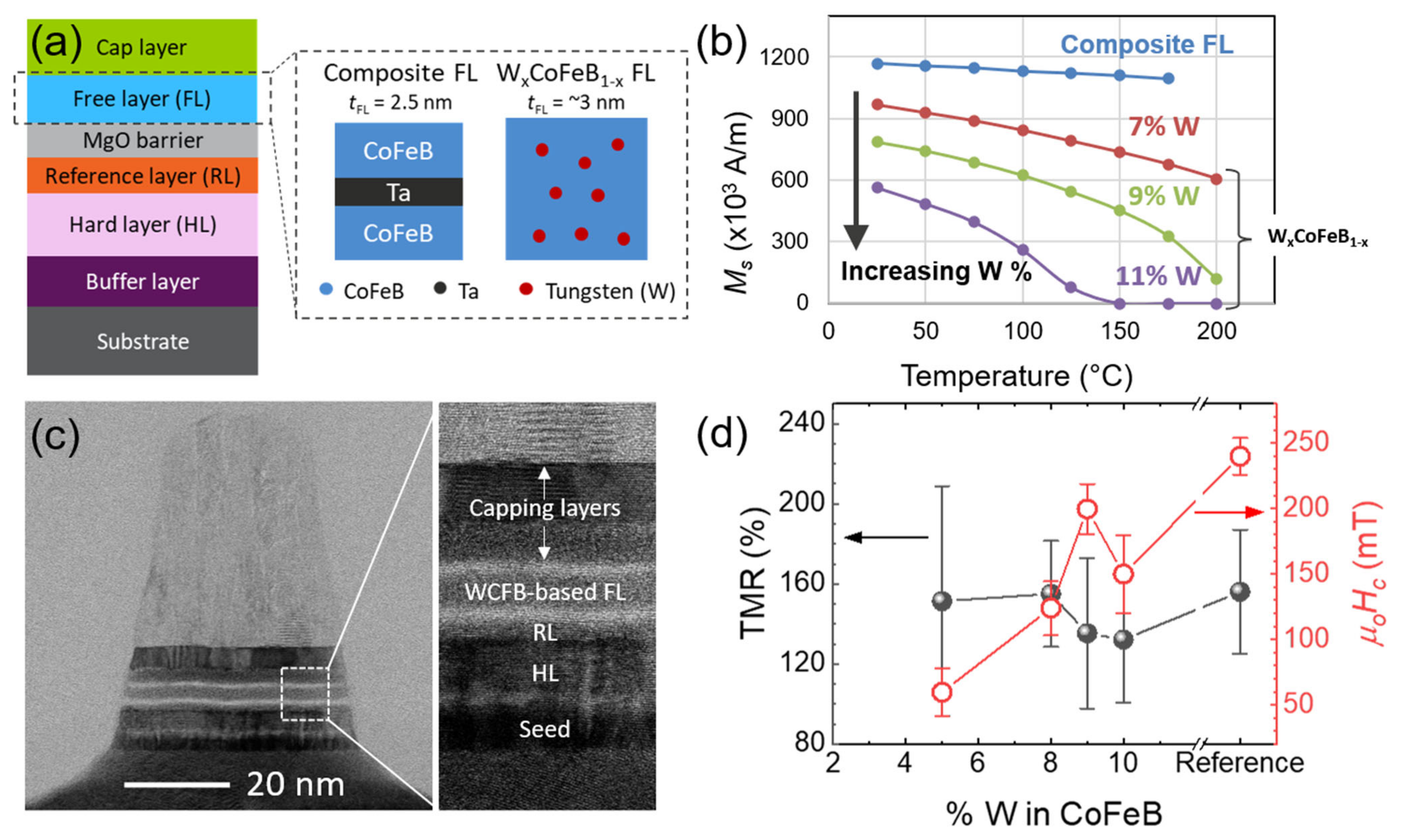
3.1. Stack Development and Fundamental MTJ Properties

Backend-of-line (BEOL) compatible bottom-pinned pMTJ stacks with two different FLs were prepared—the first, with the conventional composite FL, and the second, with the proposed FL WxCoFeB1-x (W concentration range = 5–10%). Figure 1a illustrates the schematic representation of the full pMTJ stack, and the two free layer stack combinations investigated in this study. For the composite FL stack, a Ta spacer-based design was chosen for this study instead of a W spacer-based design, owing to a ~2x reduction in damping with the former, as shown in our previous studies [23]. Thus, a Ta spacer-based composite FL is a more appropriate reference for switching current evaluation in alloyed FL designs. Prior to device fabrication, the saturation magnetization (Ms) of the film stacks is estimated by vibrating sample magnetometry (VSM) measurements for temperatures up to 200 °C. As the W concentration increases, a monotonically decreasing trend in Ms and a significant reduction in the Curie temperature (Tc) is observed, as seen in Figure 1b, in line with recent reports [20]. The STT-driven writing in scaled pMTJ devices (CD < 100 nm) is expected to result in significant self-heating in the vicinity of the MgO barrier [24]. Thus, the temperature induced Ms loss can be exploited to dynamically reduce the required switching current during the write operation while retaining its thermal stability after removing the write stress.
To evaluate this hypothesis, cylindrical devices of 50 nm CD are fabricated (see Materials and Methods). Cross-sectional TEM images, as shown in Figure 1c, at a W concentration of 9% depict a broad polycrystalline nature of the FL/MgO interface and minimal diffusion across the different layers of the pMTJ stack. To corroborate these morphological assessments, tunnel magnetoresistance (TMR) and FL coercivity (µoHc) were extracted from standard magnetoresistance measurements under the influence of an external out-of-plane (µoHext) magnetic field, as shown in Figure 1d. At a low W concentration of 5%, the measured coercivity (µoHc ~110 mT) drops steeply as compared with the composite FL reference (µoHc ~210 mT). This drop in µoHc is attributed to the degradation of the CoFeB/MgO interfacial anisotropy for longer annealing times (3 h at 400 °C). As the concentration of W increases to 10%, we observe an increase in the µoHc up to 170 mT, while TMR drops by 20% as compared with low W concentrations. This counter-intuitive observation can be understood by the impact of W doping on the crystallization of the FL from the CoFeB/MgO interface. It has been previously reported that an increase in boron (B) concentration leads to a delayed crystallization of the CoFeB/MgO interface [25,26]. The co-sputtering of W alongside CoFeB increases intermixing and limits B diffusion out of the FL. As both TMR and µoHc are dependent on the crystalline nature of the FL/MgO interface, we attribute the reduction in both metrics at W content >8% to a partially crystallized interface. By carefully tuning the W content to target the application-specific thermal budget, high TMR (>130%) and µoHc (>150 mT) metrics can be achieved.

3.2. STT Write Performance

STT-MRAM devices are typically expected to operate in the 20–200 MHz frequency range for the embedded memory market. Figure 2a,b illustrates the electrical scheme realized to enable both dc and pulsed switching measurements. We investigate the write performance for pulse durations from 2–100 ns, wherein one can expect a transition from pure precessional switching regime ( τ P W < 10 ns) to an intermediate region comprising both switching regimes ( τ P W ~10–100 ns). The switching probability (Psw) is extracted from 2000 switching events for each stack and pulse duration.
Figure 3a shows the average switching currents over the operating frequency range ( 1 / τ P W ) for the different W-based FLs as compared with the composite FL as a reference. For the 5% W-based FL, we observe a reduction in switching currents for all frequencies with respect to the reference, but this can be attributed to the significantly reduced coercivity (µoHc) reported for this FL (25% of the reference FL). As the doping concentration increases to 9% W, we observe a crossover in the switching current trends as the operating frequency increases. At τ P W = 5–10 ns, the switching currents for higher W concentrations (9% and 10%) are in line with the reference and can achieve a further 25% reduction in switching energy as τ P W reduces to 2 ns. These results can be understood in a two-fold manner, i.e., the increase in the W concentration gradually increases the effective anisotropy (Hk, eff) of the FL leading to a faster switching process in the precessional regime, while the increased thermal sensitivity of the W-based FL at higher concentrations also reduces the required switching current during the pulse application. To further corroborate these findings, we can extract a linear dependence of the form 1 / τ = A I c I c 0 between the pulse duration and the average switching currents [27]. The parameter ‘A’ is a figure of merit for the efficiency of the spin angular momentum transfer, and ‘Ic0′ is the zero-temperature critical switching current. These results are depicted in Figure 3b as a function of the W concentration in the FL. As compared with the composite FL, the efficiency for W concentration up to 8% is similar but experiences a four-fold increase for 9% W in the FL. A further increase in the W concentration results in a minor drop in the efficiency by ~10%. It must also be noted that Ic0 increases along with the efficiency reaching a local maximum at 9% W which suggests an increase in the effective FL anisotropy (Hk,eff) in line with previous reports [13]. The measured Ic trends scale in a linear fashion with FL Ms reduction for increasing W%. Damping in such FL stacks can also influence the switching metrics, although in our proposed alloyed FL design, the Ms variation under the influence of local self-heating (during write current pulse) is believed to be the dominant factor during switching [24]. Understanding damping in such FL designs would require a more extensive design of experiments in terms of W concentrations and annealing conditions, which we believe falls outside the stated scope of this study. Deterministic switching is achieved across the tested pulse duration range for the 10% W-doped FL, as shown in Figure 3c, with switching voltages (VMTJ) <0.8 V to as low as 5 ns and <1 V at 2 ns, thus reinforcing the suitability of the W-doped FL for high-speed and low power applications.
We also evaluate the operating margin between deterministic switching and the onset of ‘backhopping’, where the device is observed to switch back to its initial state in apparent opposition to the majority spin torques during the writing pulse. The observation of ‘backhopping’ is typically attributed to an unintentional STT-induced reversal of the reference layer magnetization at higher bias voltages [28,29]. Backhopping is detrimental to the market adoption of STT-MRAM devices, owing to the limitation in achievable write error rates (WER). This anomalous behaviour can be addressed either by increasing the RL/SAF pinning fields, and/or by reducing the switching current requirements of the FL to enlarge the error-free switching window. The operating margin for error-free switching is evaluated for both switching directions as a function of the pulse duration and W doping concentration, as shown in Figure 4a,b. In the thermally assisted switching regime ( τ P W ≥ 50 ns), the W-doped wafers achieve a wider operating margin with increasing W concentration as compared with the composite FL reference. In a purely precessional regime ( τ P W ≤ 10 ns), the 10% W-doped FL performs comparably to the reference FL but has a larger operating margin as the pulse duration decreases. Comparing the trends for both switching directions (AP-to-P and P-to-AP), we observe a monotonic dependence on the W concentration, though in opposite directions. This is attributed to the effective stray magnetic field seen at the FL of the devices due to contributions of the RL and SAF layers, which we believe can be resolved by careful control of the stack deposition and lithography processes. Interestingly, the average operating margin considering both switching directions is ~300 mV at τ P W = 2 ns regardless of the amount of W doping. These results confirm that W doping has a negligible impact on the stability of the RL and allows independent engineering of the MTJ stack to enable both low switching currents and robustness to backhopping.

3.3. Reliability

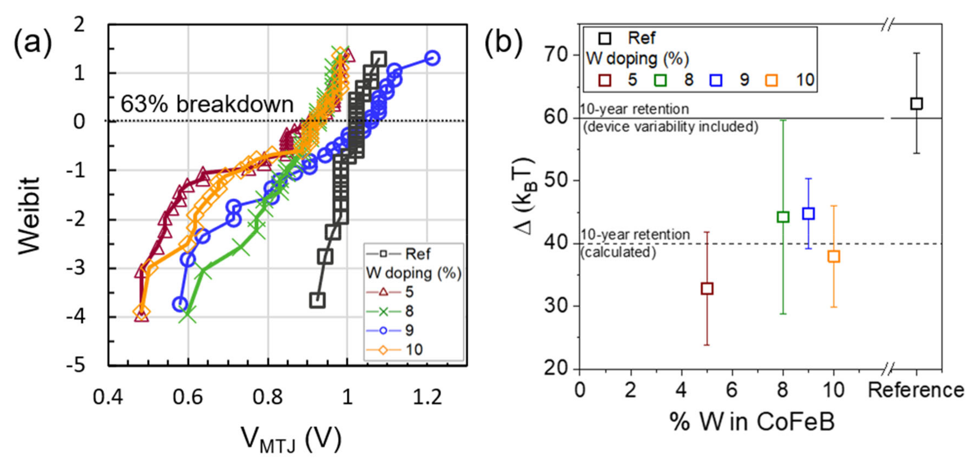
3.3.1. Breakdown Characteristics

To further investigate the impact of W doping, we evaluate the breakdown characteristics of the ~1 nm thin MgO barrier by electrically stressing the devices. The distribution of the breakdown times for a group of pMTJ devices are typically well-described by a Weibull distribution as:
F t b d = 1 exp t b d t 63 β
where tbd is the time to breakdown, β is the Weibull slope indicative of the dispersion of the breakdown times, and t63 is the mean time to failure of approximately 63.2% of all devices under test. Figure 5a depicts the Weibull distributions of the breakdown voltages estimated for different W doping concentrations under a ramped voltage stress scheme (see Materials and Methods). Each distribution is extracted from 36 randomly selected devices, allowing for an accurate estimation of the dielectric failure characteristics. As compared with the composite FL, the W-doped stacks demonstrate a 100 mV reduction in the 63% breakdown voltage (Vbd) except for the 9% W-doped wafer, where the higher Vbd is found to arise due a higher device-level R.A product (not shown). This anomalous increase in the RA is attributed to non-uniformities during the fabrication process, which is highlighted by the wider dispersion observed for the 9% W-doped wafer. The addition of W can impact the defectivity in and around the MgO dielectric barrier, which may explain the lower breakdown voltage performance. The observed bimodality in some of the distributions indicates that a careful tuning of the W content and post-patterning treatments can achieve breakdown characteristics similar to those of the composite FL alongside a write current reduction.

3.3.2. Thermal Stability and Retention

In addition to the oxide reliability, data retention is another key reliability figure of merit for STT-MRAMs to replace conventional embedded memories. The required retention time is estimated based on the hierarchical separation between the CPU and the memory storage device. Memories for the last level cache (LLC) or embedded flash (eFLASH) applications typically require ~10 years of retention time per bit of information, while those closer to the CPU require less retention times. The retention time can be estimated from a standard Arrhenius rate equation described as t r e t = t 0 e x p E b k B T = t 0 e x p Δ , where t0 is the attempt time (~1 ns), Eb is the energy barrier between the two stable states of the MTJ, kB is the Boltzmann’s constant, and T is the temperature in Kelvin. The thermal stability (Δ), expressed in the units of (kBT), is a convenient figure of merit and, hereafter, is used to describe the retention of the pMTJ devices in this paper. Figure 5b shows the thermal stability estimated from 50–100 devices for every FL stack from switching field distributions [13]. We observe a 30% reduction in Δ for the doped W-CoFeB FLs with respect to the conventional composite FL across the doping range. The reduction in Δ is attributed to the weakening of the interfacial CoFeB/MgO PMA with increasing W content, as is also seen in the coercivity trend in Figure 1d. While an estimation of the absolute Δ can also be done in the framework of a domain wall-mediated reversal model for these CDs [16], we do not expect the general trends seen in Figure 5b to change. To accurately quantify and elucidate the impact of W doping on Δ, further in-depth investigation of the temperature-dependent FL properties must be carried out. A careful optimization of the W doping content between 8 and 10% can achieve a healthy margin over the required retention specification. For memory applications closer to the CPU, this target can be further relaxed, thus falling within the scope of the W-doped FLs.

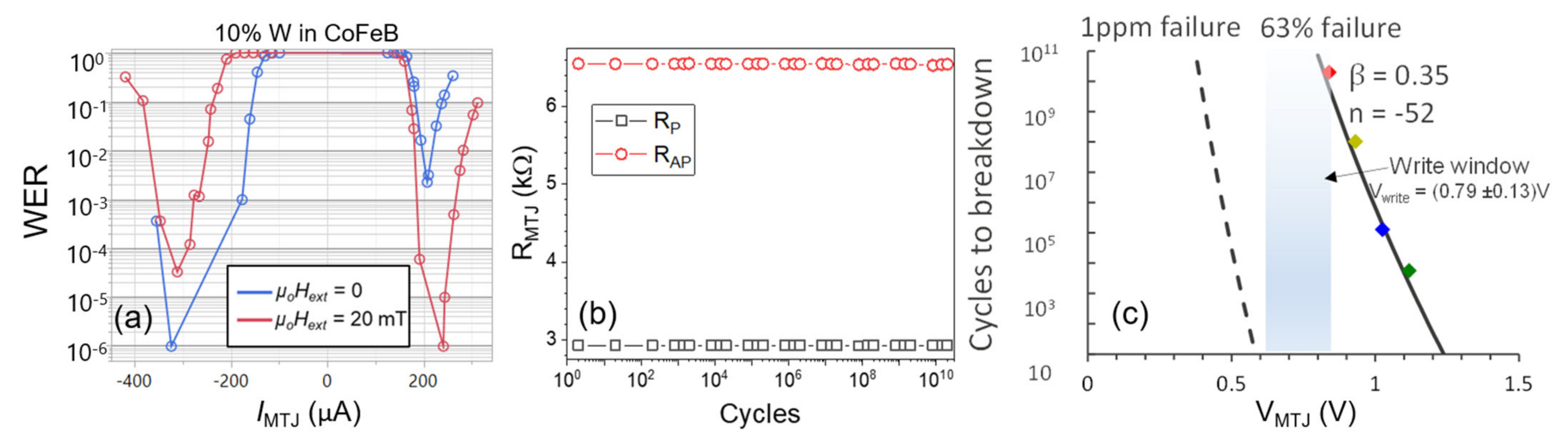
3.3.3. Write Error Rates (WER) and Endurance

To fully realize STT-MRAMs for embedded memories, it is critical to demonstrate the robustness in terms of bit error rates and endurance (or cycling). LLC applications require a minimum write error rate (WER) of one failure in 1 million write operations (or 1 ppm) and 1010–1012 cycling events. We postulated in Section 3.2 that the operating margin to backhopping is skewed due to the stray magnetic fields experienced by the FL due to the RL and SAF layers within the pMTJ device. To validate this hypothesis, we performed one million write operations with and without an external magnetic field (µoHext) to compensate the effects of the internal stray field (µoHstray ~−20 mT). As it is not feasible to demonstrate the required specifications over several stacks and devices in a realistic testing timeframe, we choose to focus on the most promising stack, which is the FL with 10% W doping concentration. Figure 6a shows the WER achieved on a single bit on the above chosen stack with and without field compensation. In the case of µoHext = 0, 1 ppm error-free write is demonstrated for P-to-AP switching, while severe backhopping for the AP-to-P switch limits the achievable WER = 2 × 10⁻³ only. By roughly compensating the stray field contribution in this device (µoHext = +20 mT), we observe a shift in the WER curves for both switching directions, i.e.,1 ppm error-free write is now achieved for AP-to-P switching, while P-to-AP switching achieves WER = 2 × 10⁻⁵. These results show that in addition to backhopping suppression, good control of the magnetic stray fields is necessary to realize 1 ppm WER with sufficient margin.
Figure 6b showcases the robustness of the proposed stack at typical write conditions ( τ P W = 5 ns); no reduction of the TMR window is observed over the course of 2 × 10¹⁰ write operations (for AP-to-P and P-to-AP independently). The 1 ppm failure rate in our devices can be extrapolated with reasonable accuracy from accelerated testing at overdrive voltages, as has been shown in the past, by fitting to a power law model [22]. Figure 6c shows the 63% failure rates extracted from cycling tests for different overdrive conditions. For the applied write bias (Vwrite, average = 0.79 V with 20% variability), it can be seen that most devices survived a write operation of at least 1010 cycles, thus, meeting all of the basic requirements for embedded memory applications.

4. Conclusions

In conclusion, we clearly demonstrate the benefits of alloying conventional FL materials such as CoFeB with nonmagnetic metals (such as W) as an alternative approach to achieve write performance improvement in STT-MRAM devices. The WxCoFeB1-x FL design is shown to achieve precise control of the FL magnetization (Ms) and its temperature dependence, in addition to enhanced thermal budgets up to 180 min at 400 °C. These effects result in a 15% reduction of the write current at short pulse widths, as low as 2 ns. While backhopping is observed in these devices, we believe the enhancement of the RL pinning fields through stronger RL/SAF coupling should address these concerns satisfactorily. A successful 1 ppm write error rate and an endurance >1010 cycles is also demonstrated at the bit level. We also propose a step-by-step optimization strategy to address the observed reduction in data retention and breakdown voltage metrics. As commercial STT-MRAM products must operate in a wide temperature range, it is of significant interest to further this study by exploring the temperature dependence of the WxCoFeB1-x FL properties to evaluate trends in thermal stability and switching behaviour. We believe that this new alloyed FL concept is of great interest to the STT-MRAM community as it presents a viable alternative route towards low power STT-MRAM coupled with a high degree of controllability in terms of production, while retaining most of its inherent advantages in terms of performance.

Author Contributions

S.C. conceptualized the stack; S.R. and S.C. designed the study; S.C., S.K., S.H.S. and N.J. supervised and/or fabricated the devices for the study; S.R., S.V.B. and S.C. performed the measurements, associated data analyses, and interpreted the findings; G.S.K. was the project leader and enabled the funding and project administration for this study; S.R. wrote the manuscript. All authors have read and agreed to the published version of the manuscript.

Funding

This work is supported by IMEC’s Industrial Affiliation Program (IIAP) on STT-MRAM devices.

Data Availability Statement

The data presented in this study are available from the corresponding author on reasonable request.

Acknowledgments

This work is supported by IMEC’s Industrial Affiliation Program (IIAP) on STT-MRAM devices. The authors would also like to acknowledge the support of IMEC’s pilot line support teams in realizing the devices for this study, and the MCA team for providing the TEM images.

Conflicts of Interest

The authors declare no conflict of interest.

References

  1. Ikeda, S.; Miura, K.; Yamamoto, H.; Mizunuma, K.; Gan, H.D.; Endo, M.; Kanai, S.; Hayakawa, J.; Matsukura, F.; Ohno, H. A Perpendicular-Anisotropy CoFeB–MgO Magnetic Tunnel Junction. Nat. Mater. 2010, 9, 721–724. [Google Scholar] [CrossRef] [PubMed]
  2. Kang, S.H. Embedded STT-MRAM for Energy-Efficient and Cost-Effective Mobile Systems. In Proceedings of the 2014 Symposium on VLSI Technology (VLSI-Technology): Digest of Technical Papers, Honolulu, HI, USA, 9–12 June 2014; pp. 1–2. [Google Scholar]
  3. Slaughter, J.M.; Rizzo, N.D.; Janesky, J.; Whig, R.; Mancoff, F.B.; Houssameddine, D.; Sun, J.J.; Aggarwal, S.; Nagel, K.; Deshpande, S.; et al. High Density ST-MRAM Technology (Invited). In Proceedings of the 2012 International Electron Devices Meeting, San Francisco, CA, USA, 10–13 December 2012; pp. 29.3.1–29.3.4. [Google Scholar]
  4. Lee, T.Y.; Yamane, K.; Otani, Y.; Zeng, D.; Kwon, J.; Lim, J.H.; Naik, V.B.; Hau, L.Y.; Chao, R.; Chung, N.L.; et al. Advanced MTJ Stack Engineering of STT-MRAM to Realize High Speed Applications. In Proceedings of the 2020 IEEE International Electron Devices Meeting (IEDM), San Francisco, CA, USA, 12–18 December 2020; pp. 11.6.1–11.6.4. [Google Scholar]
  5. Lee, Y.K.; Song, Y.; Kim, J.; Oh, S.; Bae, B.-J.; Lee, S.; Lee, J.; Pi, U.; Seo, B.; Jung, H.; et al. Embedded STT-MRAM in 28-Nm FDSOI Logic Process for Industrial MCU/IoT Application. In Proceedings of the 2018 IEEE Symposium on VLSI Technology, Honolulu, HI, USA, 18–22 June 2018; pp. 181–182. [Google Scholar]
  6. Jan, G.; Thomas, L.; Le, S.; Lee, Y.-J.; Liu, H.; Zhu, J.; Iwata-Harms, J.; Patel, S.; Tong, R.-Y.; Sundar, V.; et al. Demonstration of Ultra-Low Voltage and Ultra Low Power STT-MRAM Designed for Compatibility with 0x Node Embedded LLC Applications. In Proceedings of the 2018 IEEE Symposium on VLSI Technology, Honolulu, HI, USA, 18–12 June 2018; pp. 65–66. [Google Scholar]
  7. Naik, V.B.; Yamane, K.; Lee, T.Y.; Kwon, J.; Chao, R.; Lim, J.H.; Chung, N.L.; Behin-Aein, B.; Hau, L.Y.; Zeng, D.; et al. JEDEC-Qualified Highly Reliable 22nm FD-SOI Embedded MRAM For Low-Power Industrial-Grade, and Extended Performance Towards Automotive-Grade-1 Applications. In Proceedings of the 2020 IEEE International Electron Devices Meeting (IEDM), San Francisco, CA, USA, 12–18 December 2020; pp. 11.3.1–11.3.4. [Google Scholar]
  8. Dixit, H.; Naik, V.B.; Yamane, K.; Lee, T.; Kwon, J.-H.; Behin-Aein, B.; Soss, S.; Taylor, W.J. TCAD Device Technology Co-Optimization Workflow for Manufacturable MRAM Technology. In Proceedings of the 2020 IEEE International Electron Devices Meeting (IEDM), San Francisco, CA, USA, 12–18 December 2020; pp. 13.5.1–13.5.4. [Google Scholar]
  9. Golonzka, O.; Alzate, J.-G.; Arslan, U.; Bohr, M.; Bai, P.; Brockman, J.; Buford, B.; Connor, C.; Das, N.; Doyle, B.; et al. MRAM as Embedded Non-Volatile Memory Solution for 22FFL FinFET Technology. In Proceedings of the 2018 IEEE International Electron Devices Meeting (IEDM), San Francisco, CA, USA, 1–5 December 2018; pp. 18.1.1–18.1.4. [Google Scholar]
  10. Kan, J.J.; Park, C.; Ching, C.; Ahn, J.; Xue, L.; Wang, R.; Kontos, A.; Liang, S.; Bangar, M.; Chen, H.; et al. Systematic Validation of 2x Nm Diameter Perpendicular MTJ Arrays and MgO Barrier for Sub-10 Nm Embedded STT-MRAM with Practically Unlimited Endurance. In Proceedings of the 2016 IEEE International Electron Devices Meeting (IEDM), San Francisco, CA, USA, 3–7 December 2016; pp. 27.4.1–27.4.4. [Google Scholar]
  11. Rao, S.; Kim, W.; van Beek, S.; Kundu, S.; Perumkunnil, M.; Cosemans, S.; Yasin, F.; Couet, S.; Carpenter, R.; O’Sullivan, B.J.; et al. STT-MRAM Array Performance Improvement through Optimization of Ion Beam Etch and MTJ for Last-Level Cache Application. In Proceedings of the 2021 IEEE International Memory Workshop (IMW), Dresden, Germany, 16–19 May 2021; pp. 1–4. [Google Scholar]
  12. Xue, L.; Ching, C.; Kontos, A.; Ahn, J.; Wang, X.; Whig, R.; Tseng, H.; Howarth, J.; Hassan, S.; Chen, H.; et al. Process Optimization of Perpendicular Magnetic Tunnel Junction Arrays for Last-Level Cache beyond 7 Nm Node. In Proceedings of the 2018 IEEE Symposium on VLSI Technology, Honolulu, HI, USA, 18–12 June 2018; pp. 117–118. [Google Scholar]
  13. Khvalkovskiy, A.V.; Apalkov, D.; Watts, S.; Chepulskii, R.; Beach, R.S.; Ong, A.; Tang, X.; Driskill-Smith, A.; Butler, W.H.; Visscher, P.B.; et al. Basic Principles of STT-MRAM Cell Operation in Memory Arrays. J. Phys. D Appl. Phys. 2013, 46, 074001. [Google Scholar] [CrossRef]
  14. Liu, H.; Bedau, D.; Sun, J.Z.; Mangin, S.; Fullerton, E.E.; Katine, J.A.; Kent, A.D. Dynamics of Spin Torque Switching in All-Perpendicular Spin Valve Nanopillars. J. Mag. Mag. Mater. 2014, 358–359, 233–258. [Google Scholar] [CrossRef]
  15. Iwata-Harms, J.M.; Jan, G.; Serrano-Guisan, S.; Thomas, L.; Liu, H.; Zhu, J.; Lee, Y.-J.; Le, S.; Tong, R.-Y.; Patel, S.; et al. Ultrathin Perpendicular Magnetic Anisotropy CoFeB Free Layers for Highly Efficient, High Speed Writing in Spin-Transfer-Torque Magnetic Random Access Memory. Sci. Rep. 2019, 9, 19407. [Google Scholar] [CrossRef] [PubMed] [Green Version]
  16. Santos, T.S.; Mihajlović, G.; Smith, N.; Li, J.-L.; Carey, M.; Katine, J.A.; Terris, B.D. Ultrathin Perpendicular Free Layers for Lowering the Switching Current in STT-MRAM. J. Appl. Phys. 2020, 128, 113904. [Google Scholar] [CrossRef]
  17. Chatterjee, J.; Sousa, R.C.; Perrissin, N.; Auffret, S.; Ducruet, C.; Dieny, B. Enhanced Annealing Stability and Perpendicular Magnetic Anisotropy in Perpendicular Magnetic Tunnel Junctions Using W Layer. Appl. Phys. Lett. 2017, 110, 202401. [Google Scholar] [CrossRef] [Green Version]
  18. Hu, G.; Gottwald, M.G.; He, Q.; Park, J.H.; Lauer, G.; Nowak, J.J.; Brown, S.L.; Doris, B.; Edelstein, D.; Evarts, E.R.; et al. Key Parameters Affecting STT-MRAM Switching Efficiency and Improved Device Performance of 400 °C-Compatible p-MTJs. In Proceedings of the 2017 IEEE International Electron Devices Meeting (IEDM), San Francisco, CA, USA, 2–6 December 2017; pp. 38.3.1–38.3.4. [Google Scholar]
  19. Kan, J.J.; Gottwald, M.; Park, C.; Zhu, X.; Kang, S.H. Thermally Robust Perpendicular STT-MRAM Free Layer Films Through Capping Layer Engineering. IEEE Trans. Magn. 2015, 51, 1–5. [Google Scholar] [CrossRef]
  20. Iwata-Harms, J.M.; Jan, G.; Liu, H.; Serrano-Guisan, S.; Zhu, J.; Thomas, L.; Tong, R.-Y.; Sundar, V.; Wang, P.-K. High-Temperature Thermal Stability Driven by Magnetization Dilution in CoFeB Free Layers for Spin-Transfer-Torque Magnetic Random Access Memory. Sci. Rep. 2018, 8, 14409. [Google Scholar] [CrossRef] [PubMed]
  21. O’Sullivan, B.J.; Van Beek, S.; Roussel, P.J.; Rao, S.; Kim, W.; Couet, S.; Swerts, J.; Yasin, F.; Crotti, D.; Linten, D.; et al. Extended RVS Characterisation of STT-MRAM Devices: Enabling Detection of AP/P Switching and Breakdown. In Proceedings of the 2018 IEEE International Reliability Physics Symposium (IRPS), Burlingame, CA, USA, 11–15 March 2018; pp. P-MY.5-1–P-MY.5-6. [Google Scholar]
  22. Van Beek, S.; Rousse, P.; O’Sullivan, B.; Degraeve, R.; Cosemans, S.; Linten, D.; Kar, G.S. Study of Breakdown in STT-MRAM Using Ramped Voltage Stress and All-in-One Maximum Likelihood Fit. In Proceedings of the 2018 48th European Solid-State Device Research Conference (ESSDERC), Dresden, Germany, 3–6 September 2018; pp. 146–149. [Google Scholar]
  23. Couet, S.; Devolder, T.; Swerts, J.; Lin, T.; Liu, E.; Van Elshoct, S.; Kar, G.S. Impact of Ta and W-based spacers in double MgO STT-MRAM free layers on perpendicular anisotropy and damping. Appl. Phys. Lett. 2017, 107, 152406. [Google Scholar] [CrossRef]
  24. Van Beek, S.; O’Sullivan, B.J.; Roussel, P.J.; Degraeve, R.; Bury, E.; Swerts, J.; Couet, S.; Souriau, L.; Kundu, S.; Rao, S.; et al. Impact of Self-Heating on Reliability Predictions in STT-MRAM. In Proceedings of the 2018 IEEE International Electron Devices Meeting (IEDM), San Francisco, CA, USA, 1–5 December 2018; pp. 25.2.1–25.2.4. [Google Scholar]
  25. Endoh, T.; Honjo, H. A Recent Progress of Spintronics Devices for Integrated Circuit Applications. J. Low Power Electron. Appl. 2018, 8, 44. [Google Scholar] [CrossRef] [Green Version]
  26. Pellegren, J.P.; Furuta, M.; Sundar, V.; Liu, Y.; Zhu, J.-G.; Sokalski, V. Increased Boron Content for Wider Process Tolerance in Perpendicular MTJs. AIP Adv. 2017, 7, 055901. [Google Scholar] [CrossRef] [Green Version]
  27. Bedau, D.; Liu, H.; Sun, J.Z.; Katine, J.A.; Fullerton, E.E.; Mangin, S.; Kent, A.D. Spin-Transfer Pulse Switching: From the Dynamic to the Thermally Activated Regime. Appl. Phys. Lett. 2010, 97, 262502. [Google Scholar] [CrossRef] [Green Version]
  28. Hu, G.; Nowak, J.J.; Gottwald, M.G.; Sun, J.Z.; Houssameddine, D.; Bak, J.; Brown, S.L.; Hashemi, P.; He, Q.; Kim, J.; et al. Reliable Five-Nanosecond Writing of Spin-Transfer Torque Magnetic Random-Access Memory. IEEE Magn. Lett. 2019, 10, 1–4. [Google Scholar] [CrossRef]
  29. Kim, W.; Couet, S.; Swerts, J.; Lin, T.; Tomczak, Y.; Souriau, L.; Tsvetanova, D.; Sankaran, K.; Donadio, G.L.; Crotti, D.; et al. Experimental Observation of Back-Hopping With Reference Layer Flipping by High-Voltage Pulse in Perpendicular Magnetic Tunnel Junctions. IEEE Trans. Magn. 2016, 52, 1–4. [Google Scholar] [CrossRef]
Figure 1. (a) Schematic of the pMTJ stack and the two free layer (FL) stack options. The hard layer (HL) is a [Co/Pt]x-based multilayer, and the reference layer is a [Co/spacer/FeB]-based trilayer stack. The HL and RL are coupled through a metallic spacer to form a synthetic antiferromagnet (SAF). The composite FL serves as the reference for this study; (b) temperature dependence of the saturation magnetization (Ms) measured for the composite FL and WxCoFeB1-x FL with varying W concentrations; (c) cross-sectional TEM image of a fully fabricated 50 nm CD device with FL = W0.09(CoFeB)0.91. The zoomed-in image shows good polycrystalline order at the RL/MgO/FL/MgO interfaces; (d) tunnel magnetoresistance (TMR) and magnetic coercivity (µoHc) measured on 50 nm CD devices for varying W concentrations and the reference stack.
Electronics 10 02384 g001
Figure 2. (a) Electrical measurement scheme for dc and pulsed measurements. A Keithley K2450 and Keysight M8190A pulse generator are connected through a bias tee (up to 6 GHz) to enable fast switching and DC readout of the resistance states; (b) waveform sequence for read and write pulses. The interval time between the pulses (tinter) and integration time of the read pulse (tread) have been optimized to ensure accurate readout.
Electronics 10 02384 g002
Figure 3. (a) Comparison of average write currents at different frequencies ( 1 / τ P W ) for the different FL stack options estimated from 2000 switching events/data point; (b) extracted critical switching currents (Ic0) and spin transfer efficiency (A) as a function of W doping concentration; (c) switching probability curves on showing 100% deterministic switching across the entire pulse duration testing range (2 – 100 ns) for FL = W0.1CoFeB0.9.
Electronics 10 02384 g003
Figure 4. Absolute operating margins (Vbackhopping – Vwrite) estimated for the different FL options: (a) AP-to-P switching; (b) P-to-AP switching across the tested pulse duration range (2–100 ns). The margins are estimated from the median values of switching voltages and backhopping voltages. Negligible backhopping was observed for the 9% W-doped CoFeB FL, likely due to a stronger RL/MgO interface arising from the higher-than-expected RA product.
Electronics 10 02384 g004
Figure 5. (a) Weibull distributions of DC breakdown performance for the different FL stack options. The dotted line indicates the point where 63% of the tested devices will fail. (b) Thermal stability (in kBT) estimated from fits of room temperature (RT) switching field distributions for the different FL stack options.
Electronics 10 02384 g005
Figure 6. Reliability assessment of devices with W0.1CoFeB0.9 FL at τ P W = 5 ns: (a) Experimentally measured write error rates as a function of external magnetic field (µoHext). 1 ppm (WER = 1 × 10⁻⁶) is demonstrated for both switching directions through compensation of the stray field (µoHstray); (b) evolution of device resistances (RP, RAP) during 2 × 10¹⁰ cycling events, no TMR degradation is observed; (c) lifetime extrapolations of the tested devices for 1 ppm failure based on four independent stress tests on fresh devices. Each colour indicates the biasing voltage at which 63% of the tested devices fail.
Electronics 10 02384 g006
Publisher’s Note: MDPI stays neutral with regard to jurisdictional claims in published maps and institutional affiliations.

