1. Introduction
Many electronic and power electronic circuits include Insulated Gate Bipolar Transistors (IGBTs) [
1,
2,
3,
4]. Properties of these devices strongly depend on their internal temperature
Tj [
5,
6,
7]. This temperature exceeds ambient temperature
Ta due to thermal phenomena [
5,
8,
9]. An increase in
Tj temperature causes shortening of lifetime of semiconductor devices and changes in values of their exploitation parameters [
10,
11,
12].
Two semiconductor dies are mounted in the common case. For example, many dies of the IGBT are mounted together with the die of an anti-parallel diode. In such a case, self-heating occurs in each of the mentioned dies and additionally there are mutual thermal couplings between the two dies [
13].
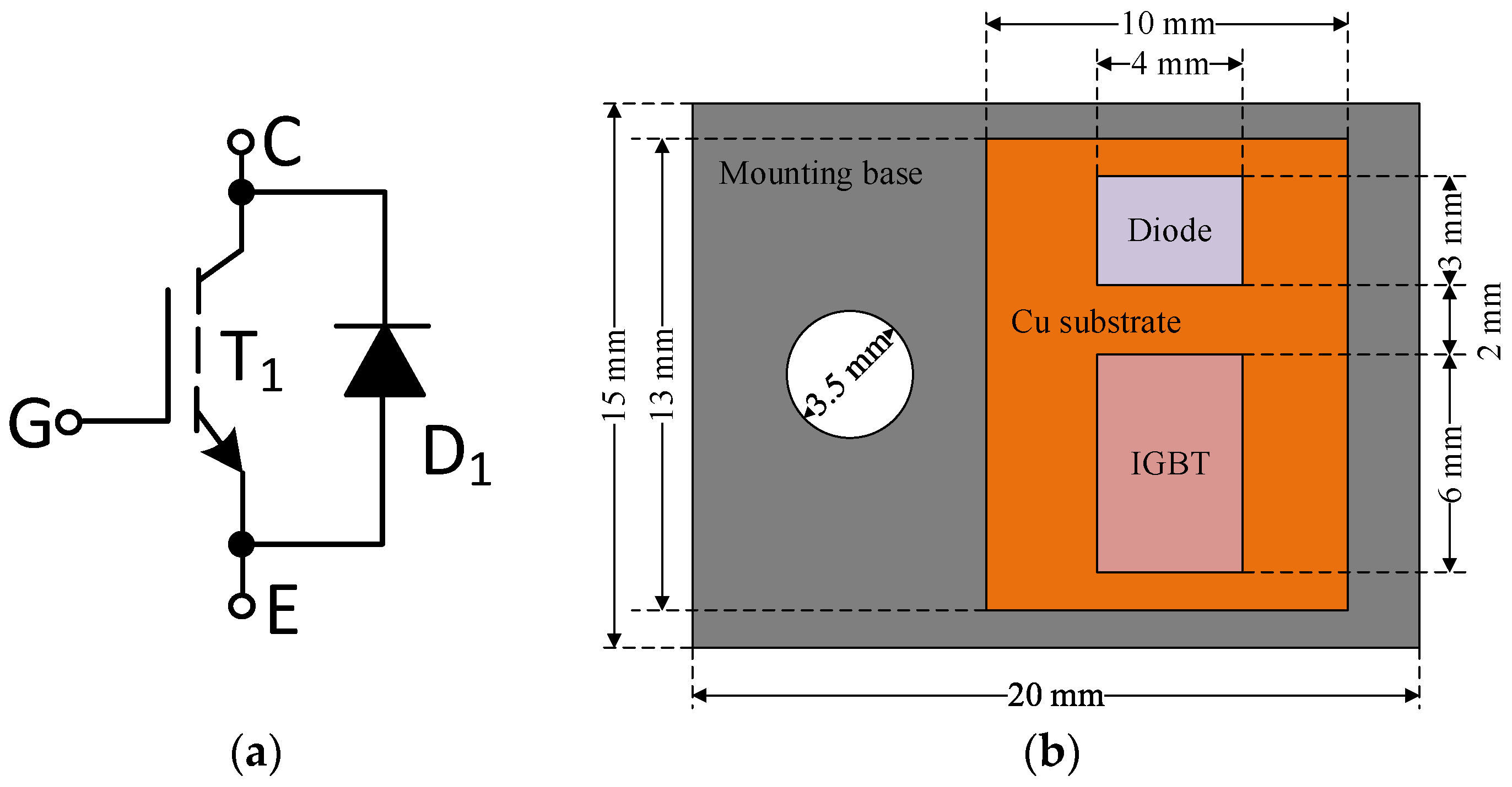
Figure 1 illustrates the schematic diagram of such a device (
Figure 1a) and a simple schematic mounting manner of the mentioned dies in the common case (
Figure 1b). As is visible, diode D
1 is connected between the collector and the emitter of transistor T
1. Both dies are soldered to Cu substrate, which makes it possible to improve heat removal generated in both dies. The area of the IGBT die is twice bigger than the area of the diode die. The distance between these dies is equal to 2 mm. Electrical connections between these dies and between lead frames and the dies are performed using bond wires. The base plate is a part of the device case.
To compute internal temperature of the semiconductor device when the value of power dissipated in this device is fixed, it is indispensable to use a thermal model of this device [
14,
15]. Compact thermal models are most frequently used [
5,
8,
13,
16,
17]. Typically, the network representation of such a model is used to describe thermal properties of semiconductor devices. A compact thermal model of a semiconductor device contains such thermal parameters as thermal resistances
Rth and thermal capacitances
Cth, which are estimated using the measured waveforms of transient thermal impedances
Zth(t). To take into account the influence of the device junction temperature on cooling efficiency, nonlinear thermal models should be used [
18].
In the formulas defining transient thermal impedance of the device, internal temperature
Tj, ambient temperature T
a and dissipated power p exist. Values of temperature
Ta and power p can be measured in an easy way, whereas the value of temperature
Tj cannot be measured directly. The value of this temperature is measured indirectly with the use of optical or electrical methods [
19,
20]. With the use of optical methods, it is possible to measure the temperature of the semiconductor die only when laboratory semiconductor devices are not in the case. In contrast, for commercially made devices, optical methods make it possible only to measure the case temperature
TC [
18], which is lower than the device internal temperature.
On the other hand, indirect electrical methods allow measuring the device internal temperature on the basis of measurements of selected electrical parameters univocally dependent on temperature. Such parameters are called thermo-sensitive parameters [
13,
16,
17,
21,
22,
23]. The literature [
17,
21,
22,
23] describes possibilities of using different thermo-sensitive parameters to measure internal temperature of different semiconductor devices. For IGBTs, the voltage between the gate and the emitter of the transistor operating in the active range, the voltage between the collector and the emitter on the switched-on transistor or the voltage on the forward biased anti-parallel diode is used [
22]. According to the JEDEC standard [
24], the recommended thermo-sensitive parameter is the voltage between the collector and the emitter on the switched-on transistor.
In all the considered measurement methods and in compact thermal models of IGBTs [
5,
17,
21,
22,
23,
25], only one internal temperature of this device is used. This temperature characterises thermal properties of the whole considered device.
An analysis of differences between values of internal temperature of the power Metal Oxide Semiconductor (MOS) transistor obtained with the use of indirect electrical methods, in which voltage on the forward biased p-n junction or threshold voltage of the transistor are thermo-sensitive parameters, is presented in [
23]. The problem of nonlinearity of thermometric characteristics while using threshold voltage as a thermo-sensitive parameter is discussed. On the basis of the results of simulations in the ANSYS software, it is shown that differences in the temperature value on the surface of the semiconductor structure of the area equal to 49 mm
2 could reach even 50 K. On the other hand, based on measurements with the electrical method and both thermo-sensitive parameters, it was observed that differences in the value of the transistor internal temperature are in the range of 4–11 K.
The authors of [
17] analysed the usefulness of selected thermo-sensitive parameters to measure internal temperature of power semiconductor devices. It is shown that the voltage on the forward biased p-n junction, through which current of a small value flows, is the most universal of the considered thermo-sensitive parameters.
Properties of measuring set-ups using different thermo-sensitive parameters of the IGBT are analysed in [
22,
23]. However, the fact that the diode and the transistor are situated in the common case, although they are separate semiconductor structures, is not taken into account [
26].
In the catalogue data of the considered class of IGBTs, the following thermal resistances are given [
26]: maximum thermal resistance junction-to-case of the IGBT (
Rthj-cIGBT), maximum thermal resistance junction-to-case of the diode (
Rthj-cD), typical thermal resistance case-to-sink (
RthCS) and maximum thermal resistance junction-to-ambient (
Rthj-a). In the catalogue data, the waveform of transient thermal impedance junction-to-case of the considered device is also given. However, the producer does not give any information about thermal parameters characterising the heat transfer between the case of the investigated device and the surroundings, because they depend on the applied cooling system of the investigated device.
As shown by the presented literature review, there is a lack of a nonlinear compact thermal model of the IGBT assembled together with the diode in the common case. Additionally, the problem of accurate measurements of internal temperatures of both dies contained in the considered devices is not studied.
In this paper, which is an extended version of the one presented in [
27], two scientific problems are considered. The first problem is the method of effective computations and measurements of internal temperatures of the IGBT and diode dies contained in the common case. To solve this problem, a nonlinear compact thermal model of such devices is proposed. The second problem is the effective method of determining parameters occurring in this model. Such a method is proposed and it uses the results of measurements of self and transfer transient thermal impedances as the input data. Additionally, the influence of the choice of a thermo-sensitive parameter on the results of measurements of the mentioned thermal parameters of the investigated device is considered. Measuring set-ups making it possible to measure thermal parameters of this model with the use of different thermo-sensitive parameters are analysed. The results of measurements of thermal parameters occurring in the thermal model and the measurements performed with the use of the considered thermo-sensitive parameters for a selected IGBT operating at different cooling conditions are compared. These measurements are performed at transients and at the steady state. The results obtained at the steady state are also compared to the results of measurements performed with the use of the optical method. The obtained results and differences in temperatures of both dies included in the common case are discussed. In comparison to the conference paper [
27], this article includes: the extended literature review, the new nonlinear compact thermal model of the investigated device, extended description of used measurement methods, results of measurements of self and transfer transient thermal impedances occurring in the elaborated model and comparison of the results of measurements to the results of computations performed with the use of the elaborated model.
2. Nonlinear Compact Thermal Model of the Investigated Device
In this paper, the IGBT containing two semiconductor dies in the common case: the transistor and the anti-parallel diode [
26] is considered. Since these dies are situated in the common case, internal temperature of each of them depends on self-heating phenomena and mutual thermal couplings between these dies [
13,
28].
To determine the value of internal temperature of each mentioned semiconductor die at the well-known power dissipated in each of them, a thermal model is used [
13,
16,
18,
29,
30]. One of the forms of such a model can be a network representation. In the literature, two typical networks representations of the compact thermal models are described: the Foster network and the Cauer network [
31,
32]. As stated in some papers (e.g., [
31,
32]), the Foster network does not have any physical interpretation, whereas the Cauer network can be obtained as a result of discretisation of the heat transfer equation. The classical form of the mentioned networks makes it possible to compute the device internal temperature with self-heating phenomena only. Additionally, in these networks, linear RC components are used and they do not make it possible to take into account the observed experimentally [
18] dependences of efficiency of heat removal on the device internal temperature.
In this section, the nonlinear compact thermal model of the considered device is proposed. This model makes it possible to compute internal temperature of the IGBT and the diode taking into account self-heating in both devices and mutual thermal coupling between them. In
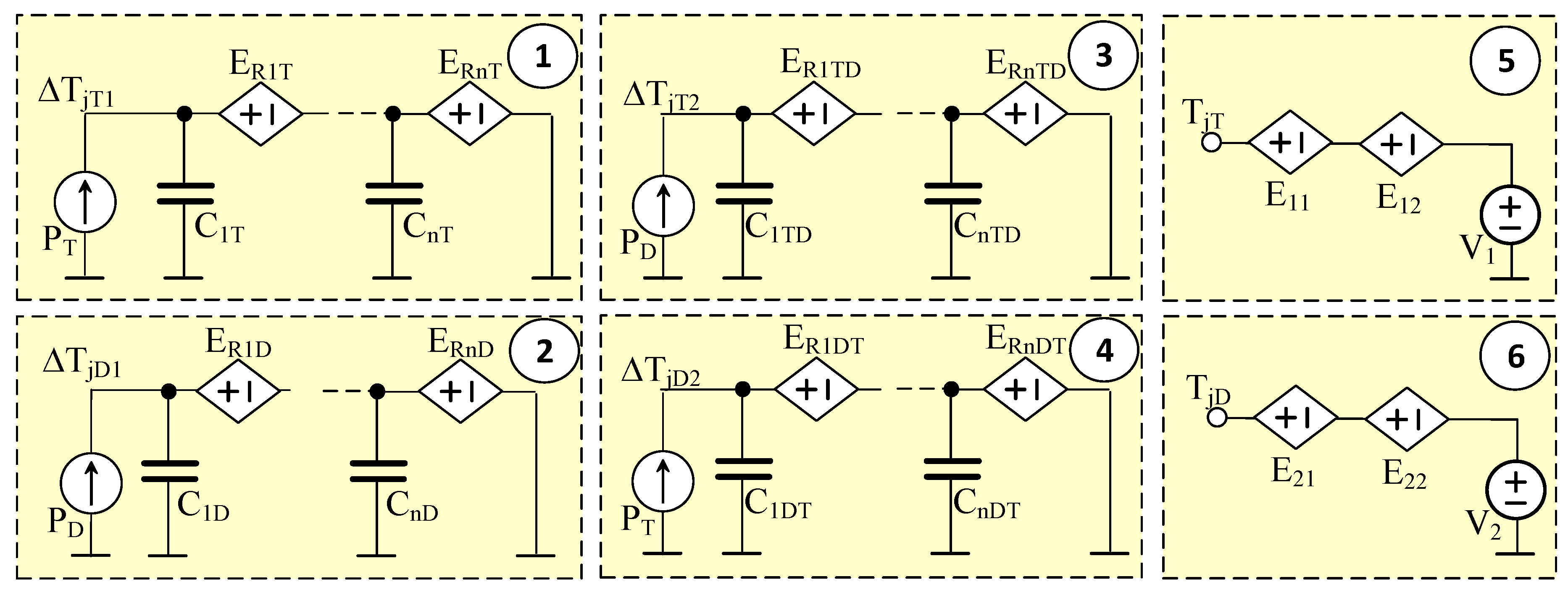
Figure 2, the network representation of the formulated model is shown.
In the proposed thermal model values of internal temperatures of the IGBT (
TjT) and the diode (
TjD) are computed taking into account self-heating phenomena in each of these devices and mutual thermal couplings between them. In the network presented in
Figure 1, six subcircuits (marked with natural numbers from 1 to 6) are visible.
Subcircuits 1 and 2 situated on the left-hand side of the figure are used to compute the value of an excess of internal temperatures of the transistor ΔTjT1 and the diode ΔTjD1 caused by self-heating phenomena in each of these devices. In these subcircuits, current sources represent power dissipated in the transistor (PT) and in the diode (PD). Capacitors C1T, CnT, C1D and CnD model thermal capacitances, whereas controlled voltage sources ER1T, ERnT, ER1D and ERnD represent thermal resistances depending on internal temperature of the dies. The mentioned components model self transient thermal impedances of the transistor ZthT(t) and the diode ZthD(t).
The next two subcircuits (3 and 4) are used to describe mutual thermal couplings between the diode and the transistor. An increase in internal temperatures of these devices is equal to ΔTjT2 and ΔTjD2, respectively. Networks containing capacitors and the controlled voltage sources occurring in the considered subcircuits represent transfer transient thermal impedance between the diode and the transistor ZthTD(t).
In the mentioned subcircuits, the controlled voltage sources describe the dependences of self and transfer thermal resistances occurring in the presented model on internal temperature of the dies included in the modelled semiconductor device. These dependences have the same form. For example, the dependence of self thermal resistance of the transistor is as follows
where
RthT0 denotes the minimum value of the considered thermal resistance,
TJT is the internal temperature of the transistor,
Ta is the ambient temperature and
RthT1 and
TZ are model parameters.
The dependences describing the output voltage of controlled voltage sources
ER1T, …,
ERnT are given by the formula
where
i is the natural number in the range from 1 to
n,
iRiT denotes current flowing through the voltage source
ERiT and
ai is the factor equal to the quotient of the part of thermal resistance occurring in
ith segment of the Cauer network and thermal resistance. The sum of all
ai factors is equal to 1.
In formulas describing self thermal resistance of the diode RthD and transfer thermal resistance between the diode and the transistor RthTD instead of temperature TjT, internal temperature of the diode TjD occurs.
Internal temperatures of the diode
TjD and the transistor
TjT are computed in subcircuits 5 and 6 shown on the right side of
Figure 1. These temperatures are equal to the sum of ambient temperature
Ta represented by voltage sources V
1 and V
2, the output voltages of controlled voltage sources E
11 and E
21 representing self-heating phenomena and the output voltages of controlled voltage sources E
12 and E
22 representing mutual thermal couplings. The output voltage of source E
11 is equal to voltage
ΔTjT1, whereas voltage E
21 is equal to voltage
ΔTjD1. In turn, the output voltages of sources E
12 and E
22 are equal to voltages
ΔTjT2 and
ΔTjD2, respectively.
All the used self and transfer transient thermal impedances take into account all the mechanisms of heat transfer between both dies and the surroundings.
To practically use the formulated thermal model, the values of parameters occurring in it must be known. The values of thermal capacitances and thermal resistances existing in this thermal model are estimated on the basis of the measured waveforms of self transient thermal impedances of the transistor and the diode and transfer transient thermal impedance between these devices. The manner of estimating the parameters of the RC Cauer network is described, e.g., in [
33]. Thermal capacitances occurring in the proposed model are directly obtained using this manner. In turn, values of parameters occurring in Equation (1) and describing self and transfer thermal resistances are obtained by an approximation of the measured dependences of these thermal resistances on internal temperatures of the dies.
The waveforms of the mentioned above transient thermal impedances are measured using indirect electrical methods. These methods are described in the next section.
3. Measurement Methods
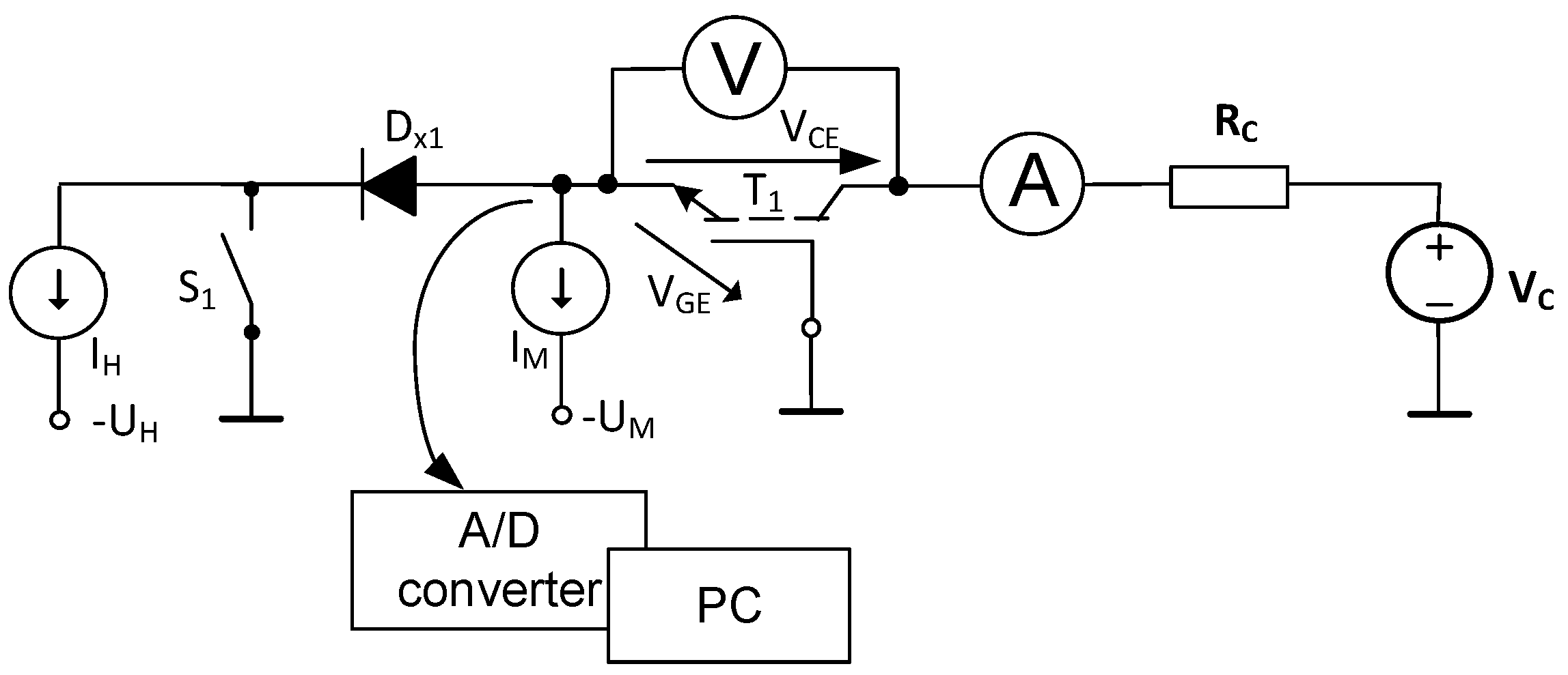
Indirect electrical methods need thermo-sensitive parameters and special measuring set-ups. In
Figure 3, the diagram of the measurement set-up of transient thermal impedance
ZthT(t) using the gate-emitter voltage
VGE as a thermo-sensitive parameter is shown. In turn, in
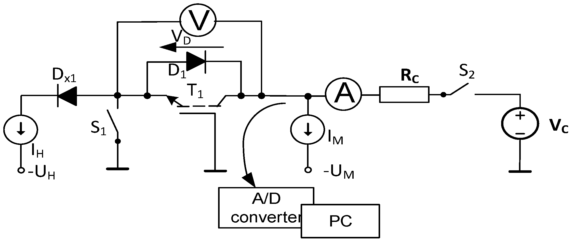
Figure 4, the measurement set-up of transfer transient thermal impedance between the transistor and the diode
ZthTD(t) using voltage on the anti-parallel diode
VD as a thermo-sensitive parameter is presented. Finally,
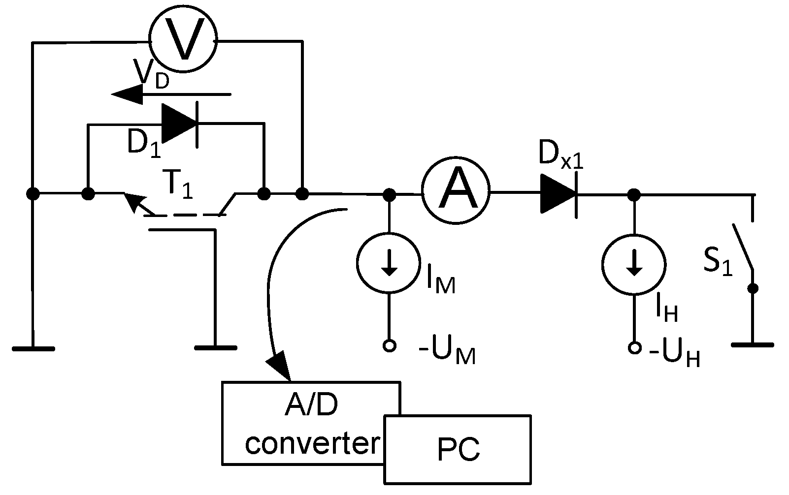
Figure 5 presents the measurement set-up of transient thermal impedance of diode
ZthD(t). In all measurement set-ups, switches are realised using power MOSFETs.
In all considered measuring set-ups, proper transient thermal impedance is determined in three steps. The first step is a calibration of the thermometric characteristic describing the dependence of a thermo-sensitive parameter on temperature TSP(T). The calibration is performed at closed switches S1 and opened switch S2. In this step, through the investigated device flows current IM of a low value. During the calibration the temperature of the transistor is regulated by means of the thermostat, wherein the investigated device is situated. From this characteristic, the slope of the thermometric characteristic is computed or an analytic formula describing the dependence of the device internal temperature on a thermo-sensitive parameter is formulated.
In the second step of measurements, heating power is dissipated in the transistor operating within the active range (
Figure 3 and
Figure 4) or in the forward biased diode (
Figure 5), and its internal temperature increases as a result of self-heating phenomena. In this stage switches S
1 are opened, and switch S
2 is closed. Through the heating device (transistor or diode) flows current
IH. This step ends after obtaining the thermally steady state. At the steady state, the value of a voltage drop of the heating device (
VCE or
VD) is measured. The value of heating power
PH is equal to the product of a voltage drop of the heating device and current
IH.
The third step begins after a change of the state of switches at time t = 0 and consists in measuring the waveform of the thermo-sensitive parameter until the steady state is obtained. Then, through the thermo-sensitive device (transistor or diode) flows current of the same value as during the calibration. The values of thermo-sensitive parameter TSEPH are measured in selected moments in time by means of the analogue-to-digital (A/D) converter and they are recorded in the computer. To stabilise the value of ambient temperature Ta during heating and cooling, the investigated device is situated in the thermostat. The value of this temperature is measured with the use of an electronic thermometer with a thermoresistor.
With the use of the thermometric characteristic
TSP(T) measured during the calibrations and the waveform of the thermo-sensitive parameter
TSEPH(t) measured in the third step of measurements, the waveform of internal temperature
Tj(t) of the thermo-sensitive device is computed. Next, proper transient thermal impedance is computed using the following formula
The value of Zth(t) obtained at the steady state is equal to thermal resistance Rth. If transient thermal impedance of the transistor ZthT(t) is measured, the waveform of temperature TjT(t) is used in Equation (3) and power PH is equal to the product of the collector current and VCE voltage. In turn, for transient thermal impedance of the diode ZthD(t), the waveform of temperature TjD(t) is used in Equation (3) and power PH is equal to the product of the diode current and VD voltage. Finally, for mutual transient thermal impedance between the transistor and the diode ZthTD(t), the waveform of temperature TjD(t) is used in Equation (3) and power PH is equal to the product of the collector current and VCE voltage.
The investigations of the method were performed for the IRG4PC40UD device. For this transistor, thermometric characteristics were measured using the forward voltage of the anti-parallel diode, the gate-emitter voltage and the collector-emitter voltage as thermally sensitive parameters. In these measurements, the value of temperature is measured with the absolute error not higher than ±1 °C and the voltages are measured with the relative error below 0.1%.
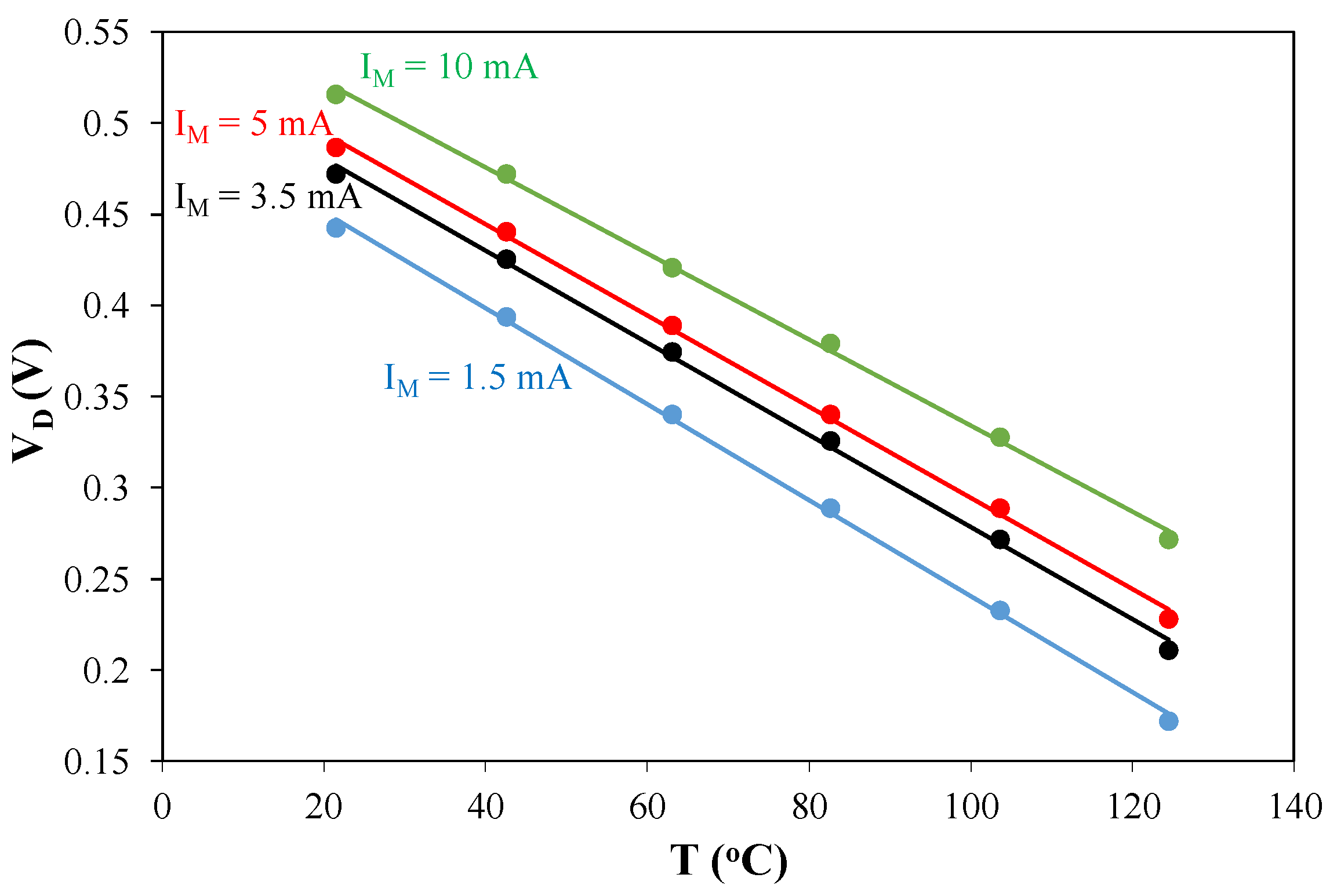
In [
27], it is shown that, for low values of forward current of the anti-parallel diode, its thermometric characteristics are nonlinear. However, there is a range of the value of this current, for which the dependence
VD(T) is linear. It is in the range from several hundred microamperes to several hundred milliamperes.
In
Figure 6, thermometric characteristics of the anti-parallel diode are shown. As can be seen, these characteristics are practically linear and their slope changes from −2.6 to −2.4 mV/K.
In turn,
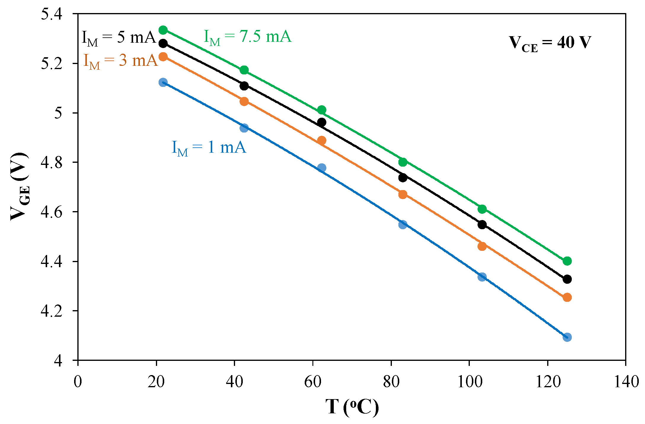
Figure 7 shows thermometric characteristics
VGE(T) measured at selected values of measurement current I
M and
VCE voltage equal to 40 V, which guarantees operation of the investigated transistor in the active mode. As is visible, these characteristics are nonlinear. They can be approximated with the use of the square function. For example, for
IM = 1 mA, this formula has the following form:
As can be noticed, characteristics VGE(T) show considerably higher (almost four times) sensitivity of the thermo-sensitive parameter at changes in temperature than characteristics VD(T). This means that, at the same accuracy of measurements of both voltages, four times higher resolution of measurements of the device internal temperature using VGE voltage as a thermo-sensitive parameter can be obtained.
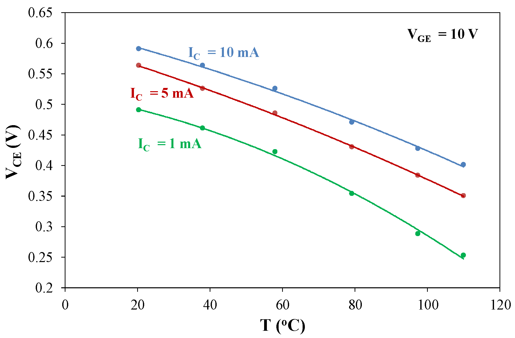
Figure 8 illustrates the dependences
VCE(T) measured at selected values of I
M current. The presented dependences were obtained at V
GE voltage equal to 10 V, which is much higher than the threshold voltage.
As is visible, the dependences VCE(T) are nonlinear for low values of the collector current (IC = 1 mA) and nearly linear for much higher values of this current. The average value of the slope of these dependences belongs to the range from −2.11 mV/K to −2.67 mV/K.
The accuracy of indirect electrical methods of measuring thermal parameters of the IGBT is analysed in [
27,
34]. Based on the considerations presented in the cited papers, the following analytical formula describing the relative error of measurements of thermal resistance
RthT can be obtained.
where Δ
TSEP, Δ
αTSEP, Δ
IH and Δ
VCE denote the absolute errors of measurements of the
TSEP, the slope of the thermometric characteristic, the current I
H and the collector-emitter voltage
VCE at the end of the second step of measurements, respectively.
Next, the value of the
TSEP is measured with the use of the fast A/D converter with the absolute measurement error equal to 2.5 mV. In turn, the error of estimating the slope of the thermometric characteristic is Δ
αTSEP ≤ 20 μV/K [
34]. The difference of the value of
TSEPH(
t = 0) −
TSEPK depends on an increase of internal temperature of the considered transistor while heating it. For example, assuming that the considered increase is equal to 100 K, the slope of the thermometric characteristic
αTSEP amounts to −2 mV/K, and the remaining errors accept the values given above; the minimum value of the error of measurements
RthT amounts to 3.7%. If an increase of temperature is equal to only 20 K, this error increases up to 13.7% [
27]. The obtained values of the measurement error are close to the values of the measurement error of thermal parameters of IGBTs performed with the optical method and computed in [
27,
34].
As shown in [
34], the accuracy of the indirect electrical method of measurements of thermal resistance of the IGBT is the highest when an increase in junction temperature over ambient temperature is the highest and the slope of the thermometric characteristic is the biggest. Analysing the thermometric characteristic shown in
Figure 6,
Figure 7 and
Figure 8, it can be easily observed that the measurement error of
ZthT(t) is the smallest if
VGE voltage is used as a thermo-sensitive parameter.
4. Investigations Results
To verify the usefulness of the proposed thermal model and the measurement method, some measurements and computations were performed. Investigations were performed for the IGBT of the type IRG4PC40UD by International Rectifier operating at different cooling conditions. This transistor is mounted in the TO-247 case and its parameters are described in [
26]. The measurements were performed for this device situated on the aluminium-heat-sink of the dimensions 78 mm × 70 mm × 34 mm and for this transistor operating without any heat-sink.
The next subsections present the results of measurements of self and transfer transient thermal impedances characterising thermal properties of the investigated device and some results of measurements and computations illustrating the non-uniformity of temperature distribution inside the investigated device. The results of measurements obtained at the steady state were compared to the results of measurements obtained with the use of the optical method.
4.1. Thermal Parameters
With the use of the measurement methods described in
Section 3, the measurements of waveforms of transient thermal impedances
ZthT(t),
ZthD(t) and
ZthTD(t) of the investigated device operating at both types of the mentioned cooling conditions were performed.
With the use of the described measurement methods and the measured thermometric characteristics, waveforms of self transient thermal impedances of the transistor
ZthT(t) and the diode
ZthD(t) and transfer transient thermal impedance between the transistor and the diode
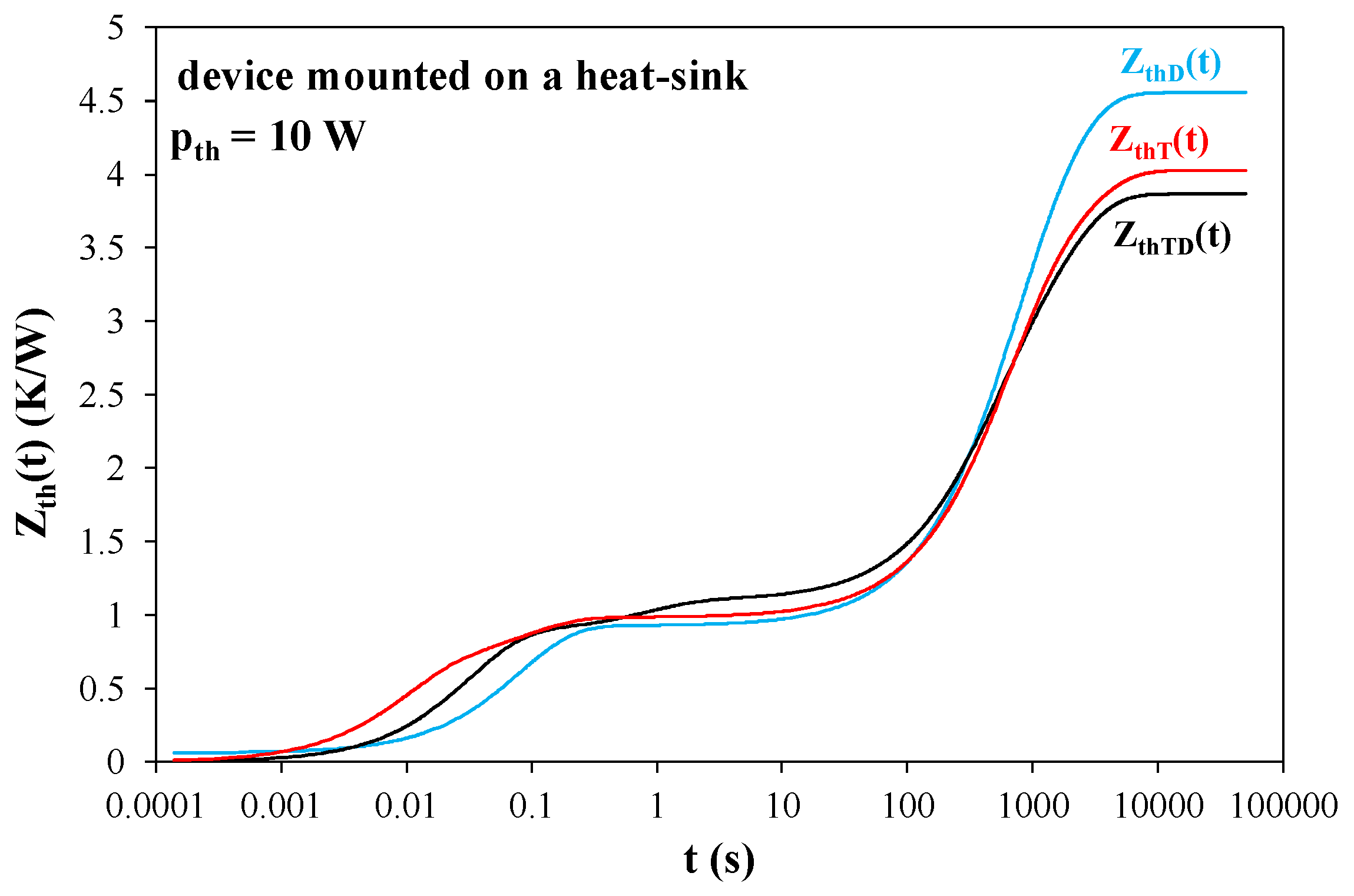
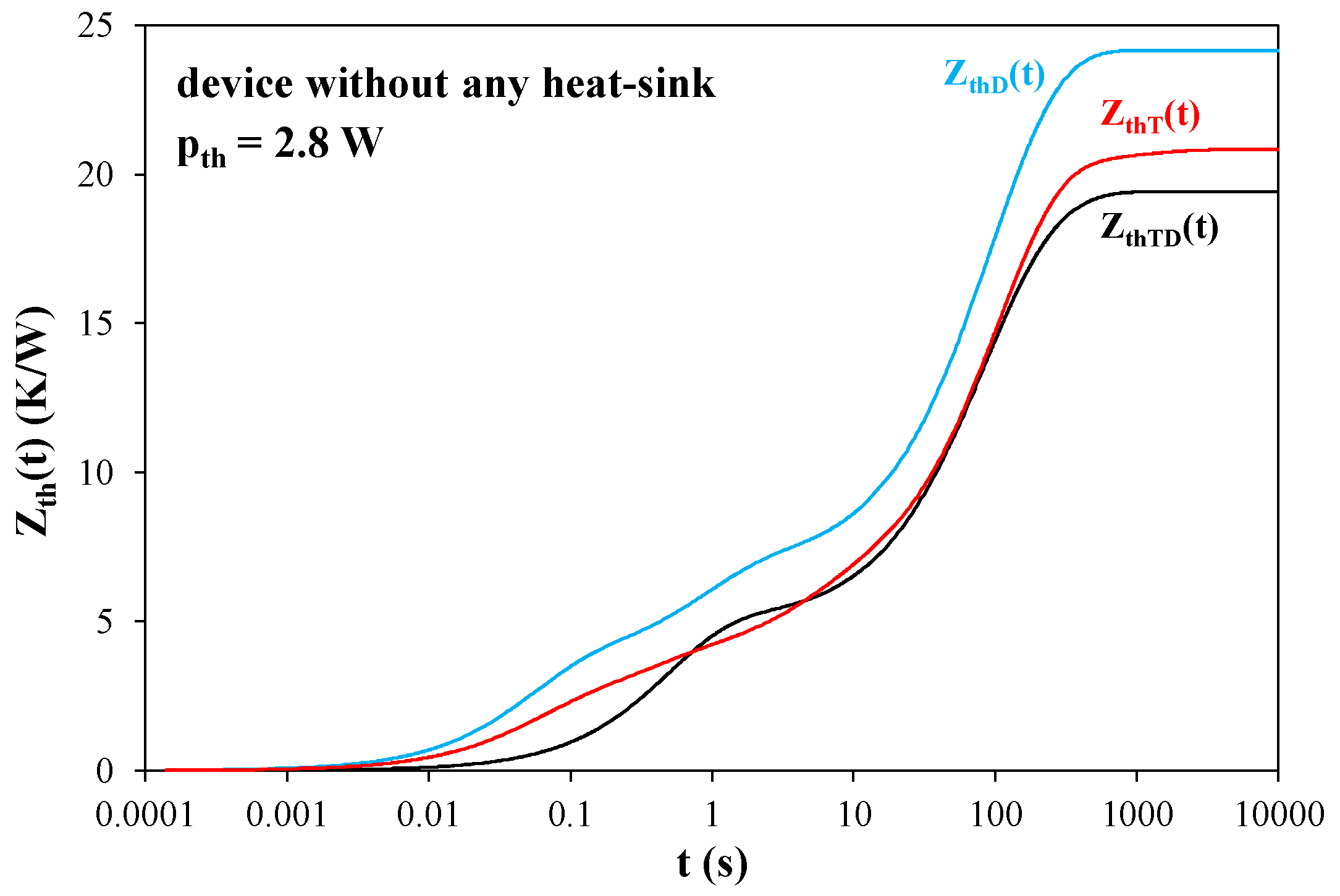
ZthTD(t) were determined. These waveforms are presented in
Figure 9 for the investigated device situated on the heat-sink and in
Figure 10 for the device operating without any heat-sink.
As can be seen, waveforms of all the measured transient thermal impedances at fixed cooling conditions have similar shapes. The highest value of the measured waveforms is obtained for ZthD(t). For the device operating on the heat-sink ZthT(t) is lower by 12% than ZthD(t), whereas for the device operating without any heat-sink the difference between the mentioned transient thermal impedances does not exceed 15%. The lowest values were measured for transfer transient thermal impedance ZthTD(t).
It is proper to notice that waveforms of transient thermal impedances measured for the device situated on the heat-sink visibly differ from these waveforms measured for the transistor operating without any heat-sink. Particularly, one can see considerably longer set-up time of waveforms measured for the transistor situated on the heat-sink and the almost fivefold difference between their values measured at the steady state. Additionally, the thermally steady state is obtained after 200 s for the device without any heat-sink and over 2000 s for this device situated on the heat-sink. It is also proper to pay attention to the fact that, for the transistor situated on the heat-sink, for the first 100 s the measured values of transient thermal impedances do not exceed the catalogue value of thermal resistance between the semiconductor die and the case of the device (1.7 K/W for the diode and 0.77 K/W for the transistor). This means that the heat-sink assures quasi-ideal cooling of the case of the device due to a high value of thermal capacitance of the heat-sink. In turn, for the device operating without any heat-sink, a continuous increase in the value of Zth(t) is visible resulting from small thermal capacitance of the case of the investigated device.
Waveforms of transient thermal impedances presented above were measured at fixed values of power dissipated in the investigated device. However, as has been shown (see, e.g., [
18]), waveforms of transient thermal impedances of the considered transistor visibly change with changes in the value of ambient temperature and internal temperature of the investigated device. For example, changes in the value of thermal resistance at the change in the value of the internal temperature equal to 100 K can exceed even 20%. As results from the measurements conducted by the authors and described in [
18], the dependence of thermal capacitances on internal temperature is omittable, but the dependence of thermal resistance on this temperature is strong. Therefore, in the further part of this section, only internal temperatures of both dies
TjT and
TjD and the case temperature
TC obtained at power dissipation only in the transistor are considered.
4.2. Computed and Measured Values of Internal Temperature
Values of internal temperatures of the dies included in the tested transistor operating in both types of considered cooling conditions are measured using the set-ups described in
Section 3 and the case temperature of this transistor is measured with the use of the pyrometer Optex PT-3S. These temperatures are also computed with the use of the thermal model proposed in
Section 2. The results of these measurements (points) and computations (solid lines) are shown in
Figure 11 and
Figure 12. They were performed at fixed ambient temperature when power was dissipated in the IGBT operating in the active mode. In these figures,
TjT describes the results of computations and measurements obtained with the use of
VGE voltage as a thermo-sensitive parameter, while
TjD corresponds to the measurements in which a thermo-sensitive parameter was voltage on the anti-parallel diode. The results of optical measurements are marked with
TC. In the case of optical measurements, the highest values of temperature on the surface of the case of the investigated transistor are registered.
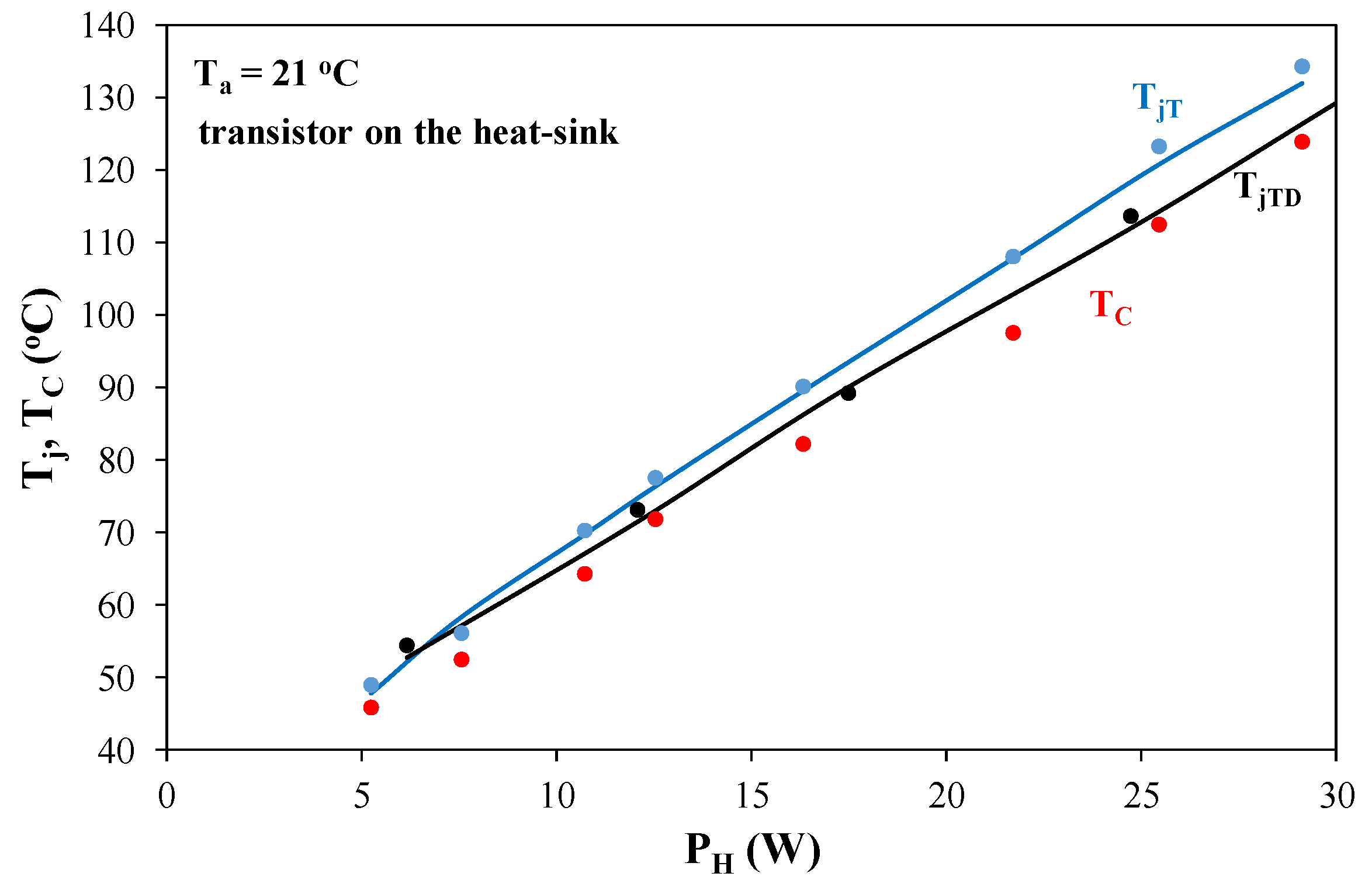
Figure 11 illustrates the measured and computed dependences of internal temperatures of both dies and the case temperature of the investigated transistor situated on the heat-sink on heating power
PH dissipated in this transistor.
As can be observed, all the considered dependences are increasing functions. Differences between values of the considered device increase together with an increase in power, attaining maximally 10 °C between the transistor internal temperature TjT and the case temperature TC. The internal temperature of the diode TjTD is lower than temperature TjT by not more than 7 °C. The results of computations and measurements differ between each other by not more than 2 °C.
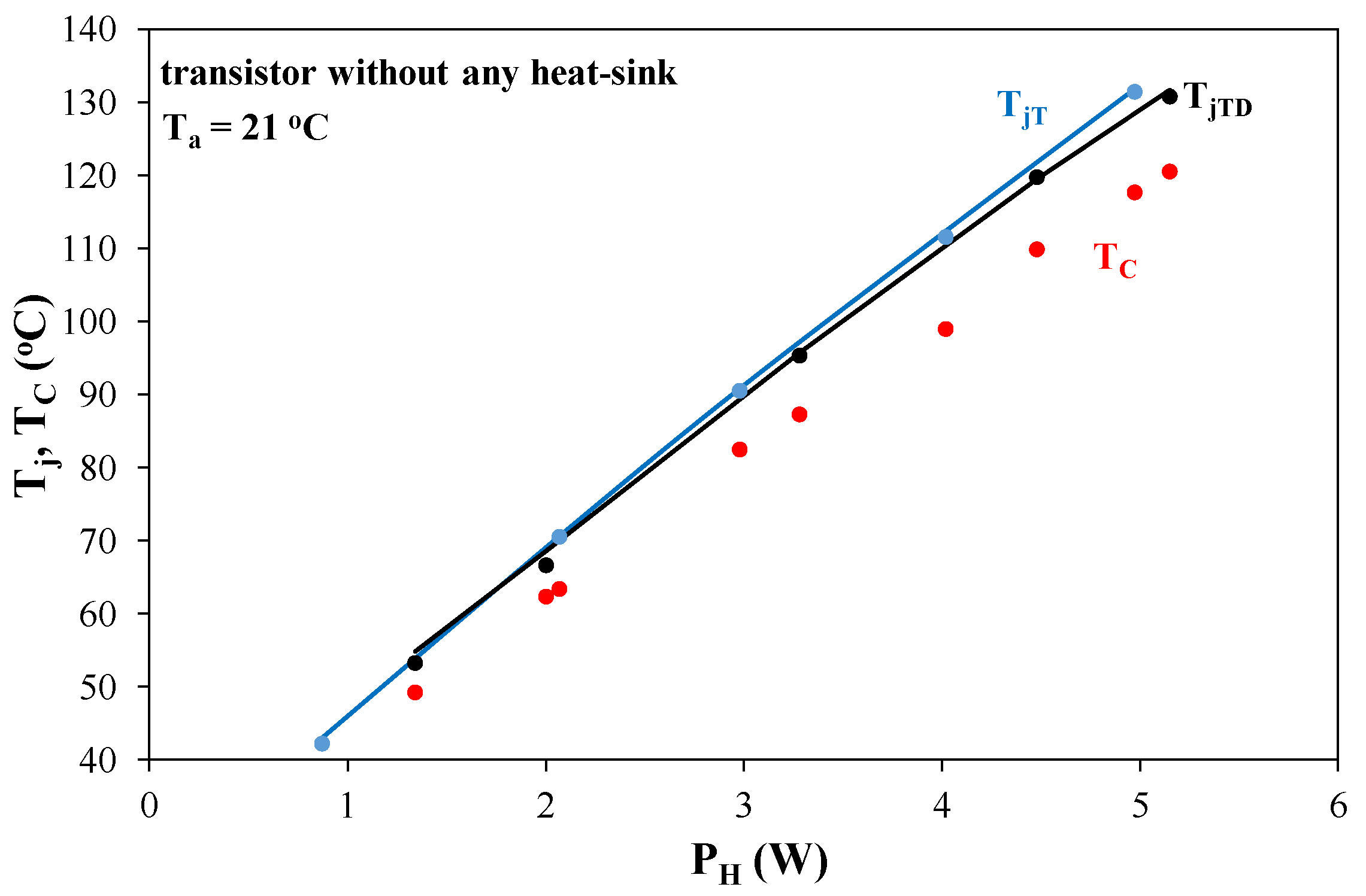
In
Figure 12, the dependences of the internal temperature and the case temperature of the investigated device operating without any heat-sink on heating power dissipated in the transistor are illustrated.
The obtained dependences of temperatures TjT, TjTD and TC on heating power are monotonically increasing functions. Differences between the obtained values of temperatures TjT and TjTD are not high, and they do not exceed 3 K. In turn, the measured values of the case temperature TC are lower than temperature TjT even by 10 °C. The results of computations fit well the results of measurements. Differences between these results do not exceed 2 °C. Such small differences prove the correctness of the proposed thermal model of the considered devices.
As can be observed, good agreement between the results of measurements and modelling is obtained in a wide range of the internal temperature of both dies (
TjT and
TjD) from 40 to >130 °C. The high border of this range is near the maximum allowable value of the internal temperature of this device, which is equal to 150 °C [
26]. This means that the thermal mode proposed by us is usable in the whole range of the allowable internal temperature of the investigated device. Differences between the results of measurements and computations do not exceed the value of the measurement error.
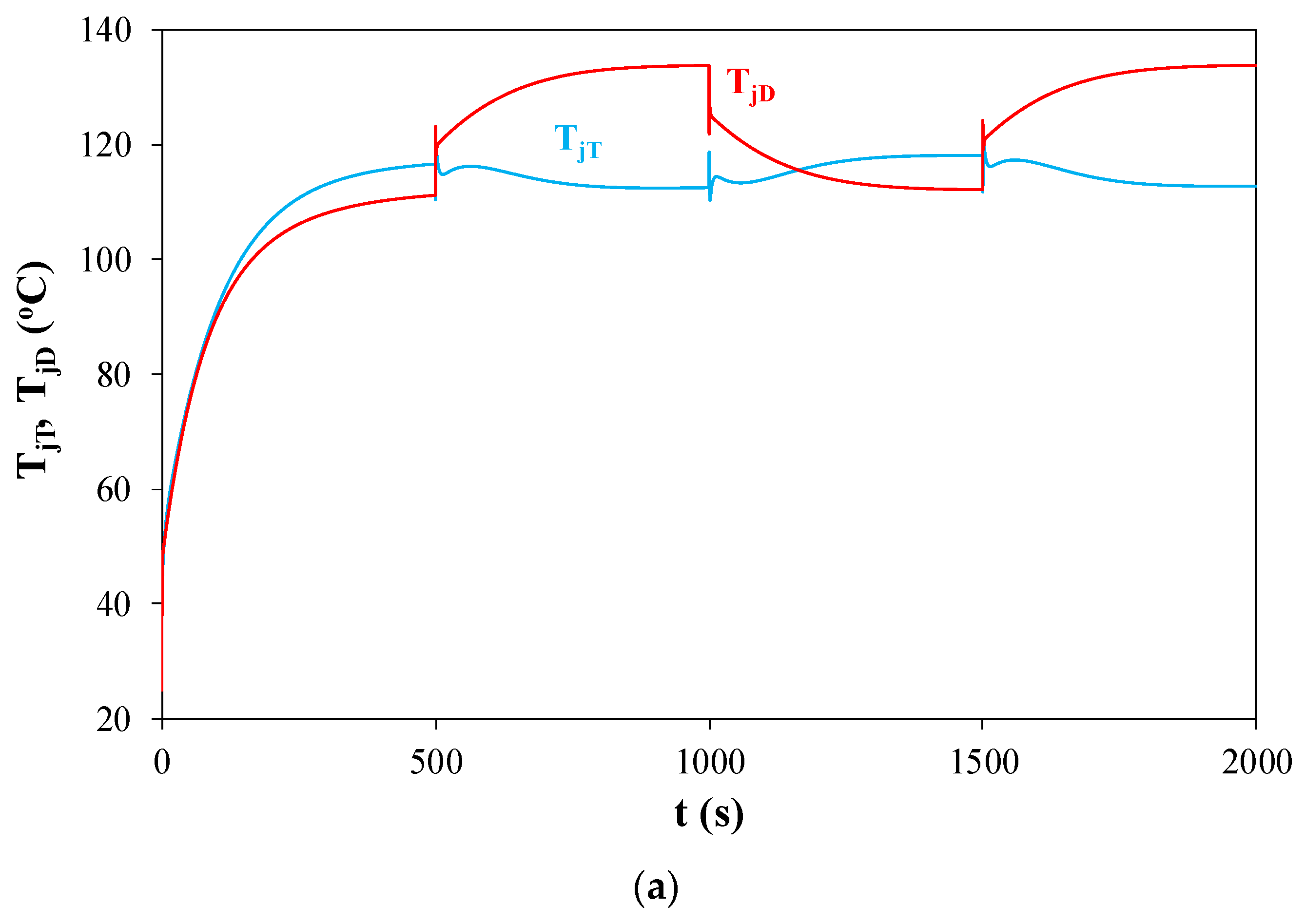
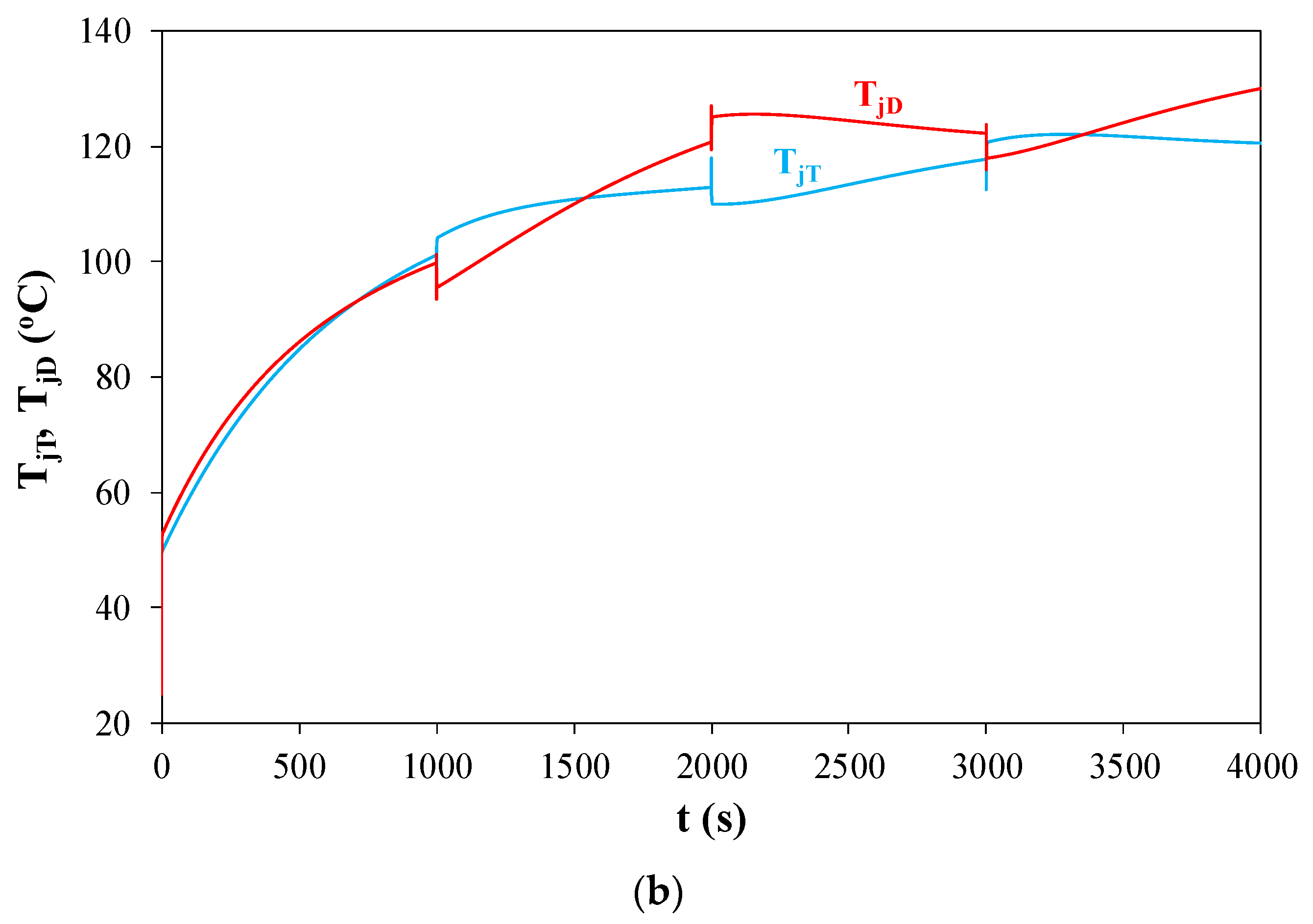
In
Figure 13, the waveforms of internal temperatures
TjT and
TjD computed with the use of the proposed model are shown.
Figure 13a presents the results of investigations performed for the tested device operating without any heat-sink, whereas
Figure 13b presents the results for the device situated on the heat-sink. The computations were performed for rectangular pulses trains of the duty cycle equal to 0.5 of power dissipated alternatively in the IGBT and in the diode. For the investigated device, the power dissipated in the transistor is shifted by half of the period in relation to the power dissipated in the diode. For the device without any heat-sink the amplitude of the dissipated power is equal to 4.5 W and the period is equal to 1000 s, whereas for the device situated on the heat-sink this amplitude amounts to 25 W and the period is 2000 s.
As can be observed, due to mutual thermal couplings, the internal temperature of the IGBT and the diode differ between each other by not more than by 20 °C. For the investigated device operating without any heat-sink for the period of time in which power is dissipated in the diode, temperature TjD is visibly higher than temperature TjT. This is a result of the higher value of RthD than RthT. When power is dissipated in the IGBT, temperature TjT exceeds temperature TjD after about 100 s after switching the power. In this case, the difference TjT − TjD does not exceed 8 °C.
Similar relations between the waveforms TjT(t) and TjD(t) can be observed for the investigated devices situated on the heat-sink. The obtained differences TjD − TjT do not exceed 15 °C.
5. Conclusions
In the paper, the problem of effective modelling and measuring thermal properties of the power semiconductor device containing the IGBT and the diode in the common case is discussed. The nonlinear compact thermal model of these devices is proposed and the manner of estimating parameters of this model is described. This manner uses indirect electrical methods and different thermo-sensitive parameters.
On the basis of the obtained results, it is stated that thermometric characteristics VGE(T) are nonlinear and can be approximated with good accuracy by a square function. In turn, thermometric characteristics VCE(T) are practically linear. The slope of the characteristic VGE(T) is even twice bigger than the slope of the characteristic VCE(T). This means that with the use of voltage VGE it is possible to obtain a lower value of the measurement error of thermal resistance than with the use of voltage VCE.
Using the considered electrical methods, self and transfer transient thermal impedances occurring in the thermal model of the power IGBT were measured for different cooling conditions of the investigated devices. Analysing the obtained results of measurements, it is easy to observe that transient thermal impedances ZthT(t), ZthTD(t) and ZthD(t) visibly differ from one another. Differences between these parameters at the steady state can reach even 15%. This result shows that a thermal model of the IGBT containing dies of the transistor and the diode in the common case should take into account two internal temperatures of this device—one characterising internal temperature of the IGBT and the other internal temperature of the diode. Differences in the values of these temperatures can reach even 20 °C.
The obtained results of measurements of internal temperatures of the IGBT and the diode when power is dissipated in the IGBT only differ slightly between each other. These differences do not exceed 10 °C due to a small difference between thermal resistance of the IGBT and transfer thermal resistance between the IGBT and the diode. Much bigger differences are observed if power is dissipated in the diode. The observed differences in the internal temperature of both dies contained in the investigated device prove that the highest temperature in this device can be observed in the diode. Therefore, it is very important to measure the internal temperature of both dies in order to verify that the investigated device operates in SOA. Additionally, the highest value of the device internal temperature affects its reliability.
The proposed compact thermal model makes it possible to more accurately model thermal properties of the investigated devices. The presented results of measurements and computations prove the usefulness of this model. The high accuracy of the proposed model in a wide range of dissipated power was obtained because the dependences of self and transfer thermal resistances on the device internal temperatures were taken into account. It is proved that the thermal model proposed in this paper is usable in the whole range of the allowable internal temperature of the investigated device.
In the article, only the thermal model of the IGBT co-packed with the diode is proposed. To perform simulations of circuits containing these two components, it is necessary to elaborate an electrothermal model of the considered device, which has to contain a thermal model and an electrical model of this device describing relationships between the device currents and voltages. The authors are currently working on such an electrothermal model.


