Article

CCSDS 131.2-B-1 Transmitter Design on FPGA with Adaptive Coding and Modulation Schemes for Satellite Communications

by
Adrián Lamoral Coines
* and
Víctor P. Gil Jiménez
Signal Theory and Communications Department, University Carlos III Madrid, 28903 Madrid, Spain
*
Author to whom correspondence should be addressed.
Electronics 2021, 10(20), 2476; https://doi.org/10.3390/electronics10202476
Submission received: 8 September 2021 / Revised: 1 October 2021 / Accepted: 4 October 2021 / Published: 12 October 2021
(This article belongs to the Special Issue System-on-Chip (SoC) Design and Its Applications)

Abstract

:
Satellite communications are a well-established research area in which the main innovation of last decade has been the use of multi-carrier modulations and more robust channel coding techniques. However, in recent years, novel advanced signal processing has started being developed for these communications due to the increase in the signal processing capacity of transmitters and receivers. Although signal processing capabilities are increasing, they are still constrained by large limitations because these techniques need to be implemented in real hardware, thus making complexity a matter of critical importance. Therefore, this paper presents the design and implementation of a transmitter with adaptable coding and modulation on a field-programmable-gate-array (FPGA). The main motivation came from the standard CCSDS 131.2-B-1 which recommends that such a novel transmitter which has to date not been implemented in a real system The system was modeled by MATLAB with the purpose of being programmed in VHDL following the AXI-stream protocol between components. Behavioral simulation results were obtained in VIVADO and compared with MATLAB for verification purposes. The transmitter logical circuit was synthesized in a FPGA Zynq Ultrascale RFSoC ZU28DR, showing low resource consumption and correct functioning, leading us to conclude that the deployment of new communication systems in state-of-the-art hardware in satellite communications is justified.

1. Introduction

In the last decade, the amount of data acquired by Earth observation satellites has been steadily increasing due to improvements in the resolution of on-board instruments, which translates into a greater capacity request in downlink data from a wireless communication link [1]. As the number of instruments on board have been increasing, maximization over downlink data rate and the application of bandwidth-efficient modulation schemes stand out as active research lines in satellite communications. In 2012, the Consultative Committee for Space Data Systems (CCSDS) published a recommendation of standard CCSDS 131.2-B-1 [2], which describes a spectrally efficient and high data-rate telemetry transmission scheme based on Serial Concatenated Convolution Codes (SCCC) [3]. Specifically, CCSDS 131.2-B-1 presents a variable and adaptive coding and modulation (VCM/ACM) plan composed of 27 transmission schemes with the goal of adapting communications according to the downlink channel [4]. Until today, CCSDS 131.2-B-1 has been regarded as a relatively new standard, generating little research attention. However, it is strongly endorsed by the European Space Agency (ESA) for next-generation applications in space communications [5].
On the other hand, new space technologies are pushing for a more efficient and faster methodology to design and develop novel communication systems embedded on satellites. An interesting proposal is the implementation of the whole system on chip (SoC). This strategy is quite risky due to the hazardous space environment that can impair the reliability-sensitive communication systems. The Soc paradigm imposes that part of the system (or the whole one) is implemented in software on a micro-processor, while the other part (or even the full system) is described in hardware on a field-programmable gate array (FPGA) [6]. In the case of satellite systems, this is a delicate task because the hostile space environment leaves the embedded software unreliable. In order to create a flexible system which is at the same time reprogrammable, compact and low weight, as well as high-speed, the project Madrid Flight on Chip [7] proposes the implementation of such a system on FPGA hardware.
Adaptive communication methods have been studied for low-Earth-orbit satellites in the literature [8,9]. In [4], an adaptive coding and modulation (ACM) scheme was shown with 27 modes, and later standardized by the Consultative Committee for Space Data Systems (CCSDS) in [2].
This paper proposes the synthesis and verification of the traditional 27 modes system specified in [2] where interconnection takes place using the AXI-stream protocol [10]. To the best of the authors’ knowledge, this is the first demonstration of an adaptive transmitter in the literature based on the CCDS standard. Modern adaptive communication systems usually require high computation power to meet speed requirements and enhance throughput. FPGAs are the most popular platforms for systems that require great performance and flexibility [11,12].
This paper is structured in the following way: firstly, the transmitter structure is detailed. Secondly, the algorithms are written and verified by MATLAB simulations. Once the MATLAB code was developed, the VHDL code was written to achieve a hardware design. Lastly, some behavioral simulations in VIVADO verify the correct RTL implementation of the transmitter.
The main contributions of this paper are:
  • A flexible FPGA design and implementation for an adaptive transmitter for high-speed satellite telemetry following standard CCSDS 131.2-B.1;
  • The optimization of the system design;
  • Validation of the design with a reference model.
The remaining parts of this paper are organized as follows. Section 2 presents the transmitter structure with ACM. Section 3 discusses the flexible and adaptive embedded prototype of the transmitter structure. Section 4 shows the simulation results from VIVADO. Finally, Section 5 states the conclusions drawn from the research.

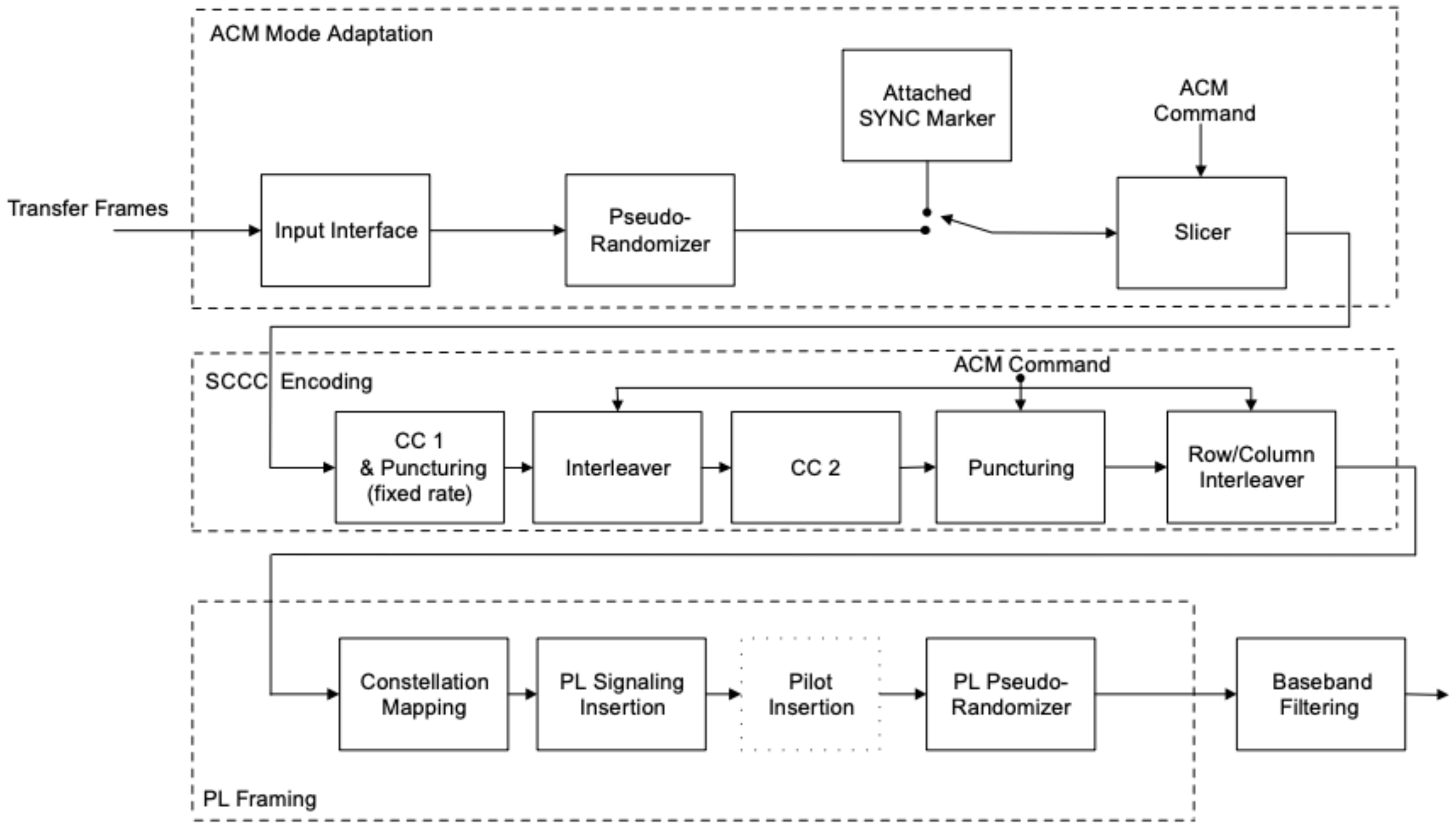
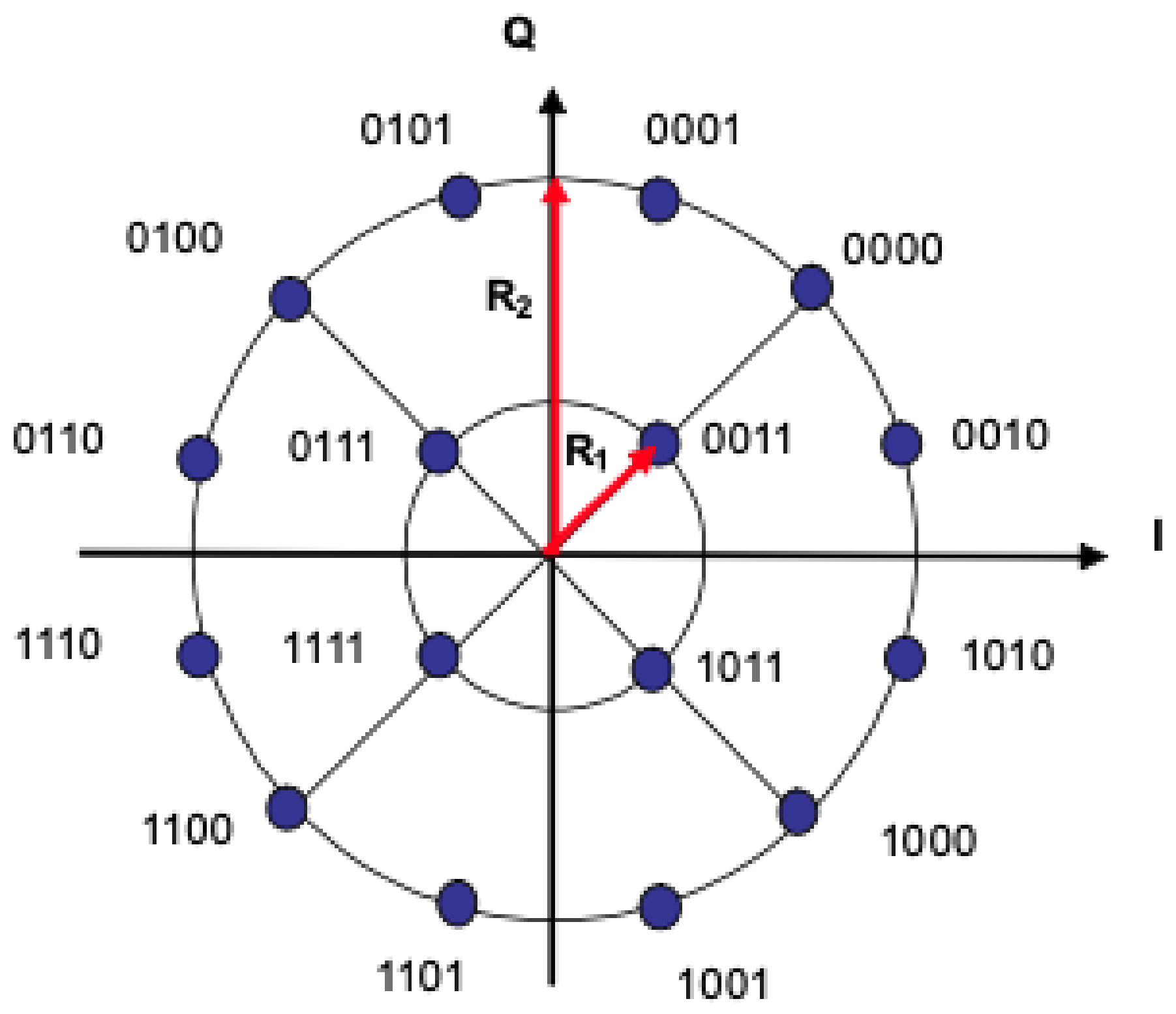
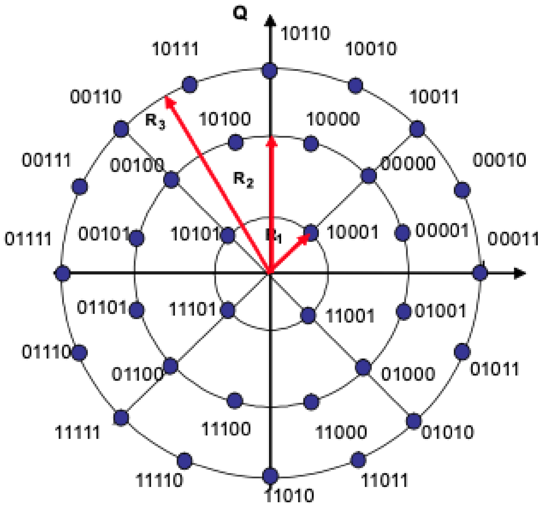
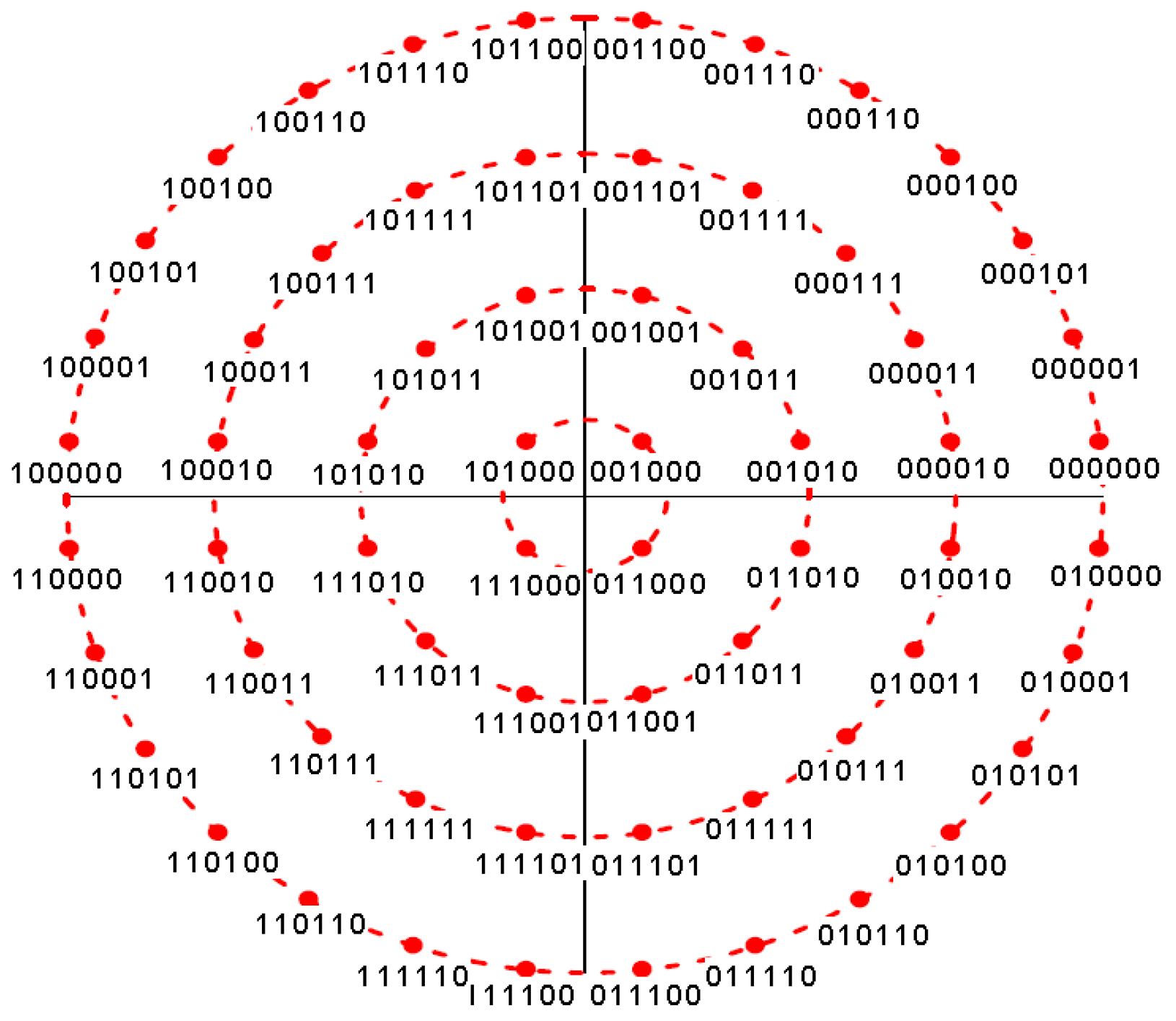
2. High Data Rate Modulator Design Description

The developed ACM transmitter structure is divided into four parts: mode adaptation; serial concatenated convolutional codes; physical layer framing; and baseband filtering. The detailed block diagram is shown in Figure 1. An ACM Command input to a given block will reconfigure its parameters and functionality according to one of the 27 available operational modes [2]. The different modes have a different configuration for the parameters and include different options and blocks in Figure 1. The different modes are used depending on the needs, the channel conditions and the status of the transmitter.
The parameters that can be changed according to the selected ACM format are given in Figure A1 located in the appendix:
  • ACM_format denotes the operational mode for the current frame;
  • m denotes the modulation order of constellation symbols;
  • S s u r denotes the number of surviving bits after CC2 puncturing in each input 300-bit segment of systematic bits;
  • K is the slicer output block length;
  • I is the interleaver block length;
  • S is the total number of transmitted systematic bits;
  • P is the total number of transmitted parity-check bits;
  • N is the row/column interleaver total block size;
  • Δ is the number of deleted parity bits in CC2 puncturing.

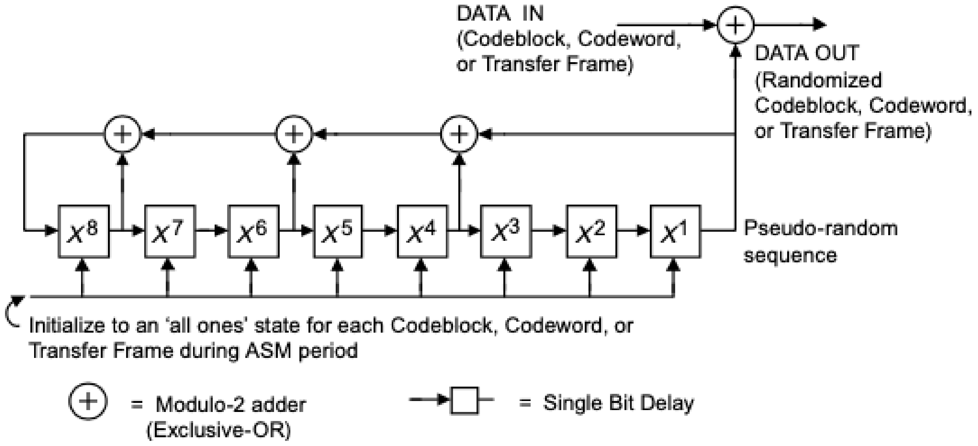
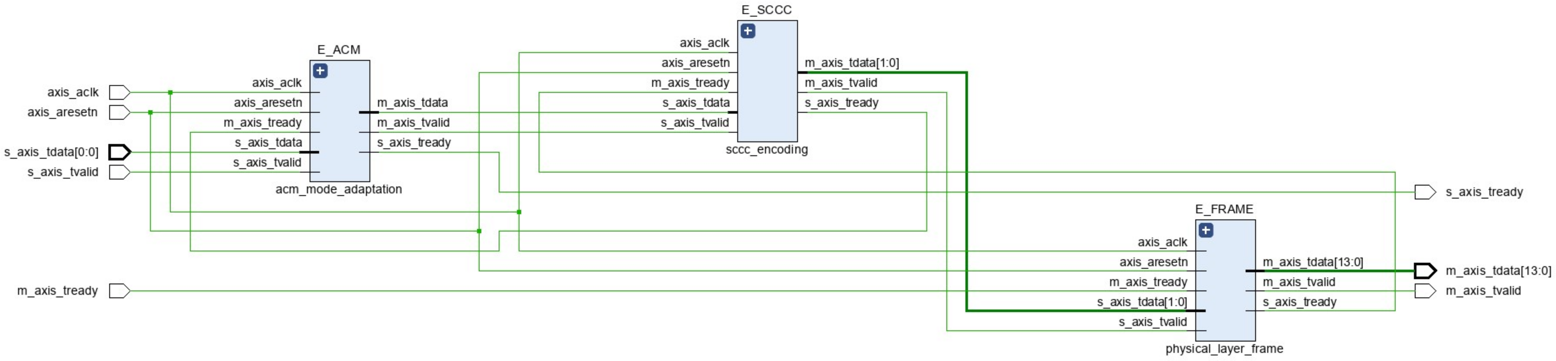
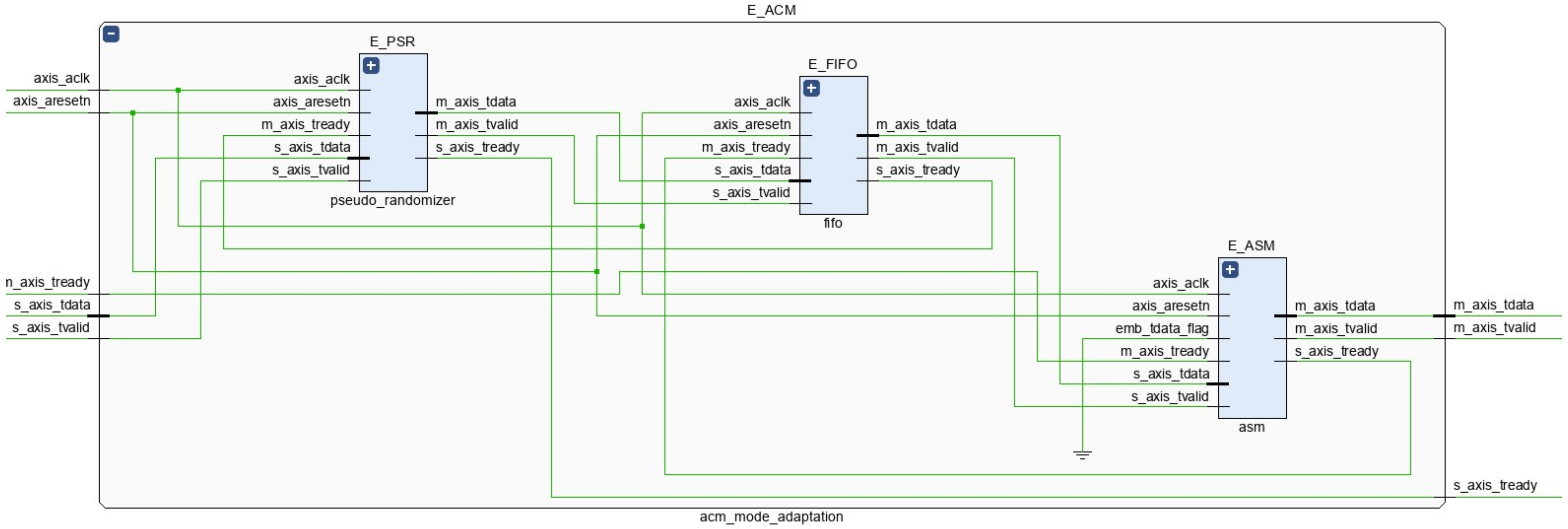
2.1. ACM Mode Adaptation
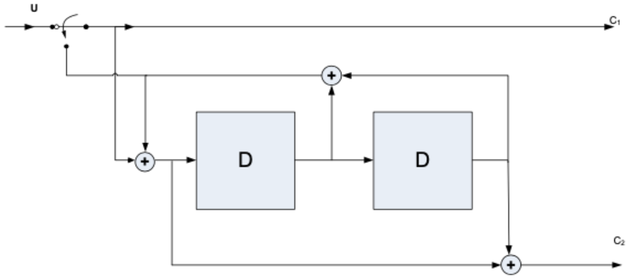
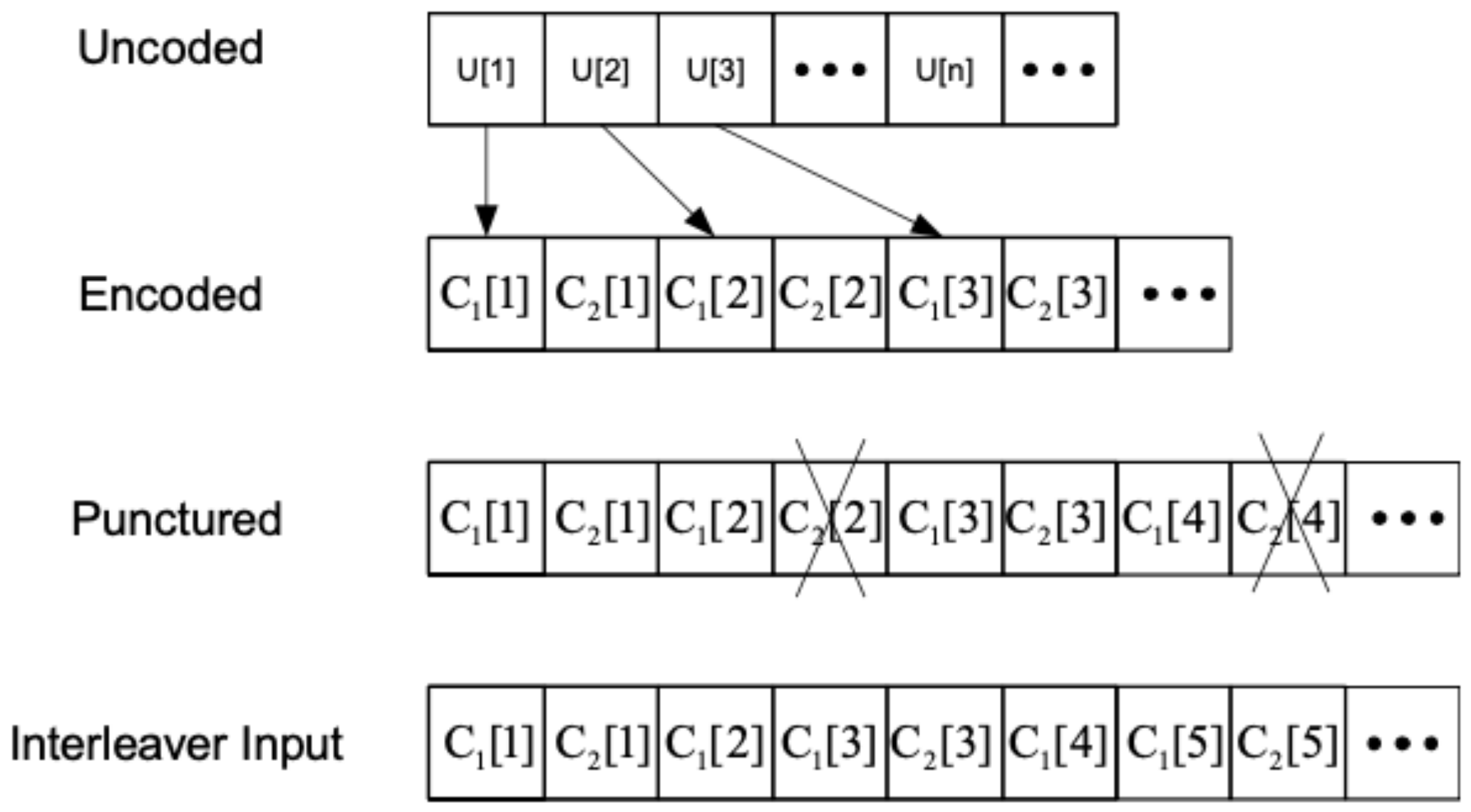
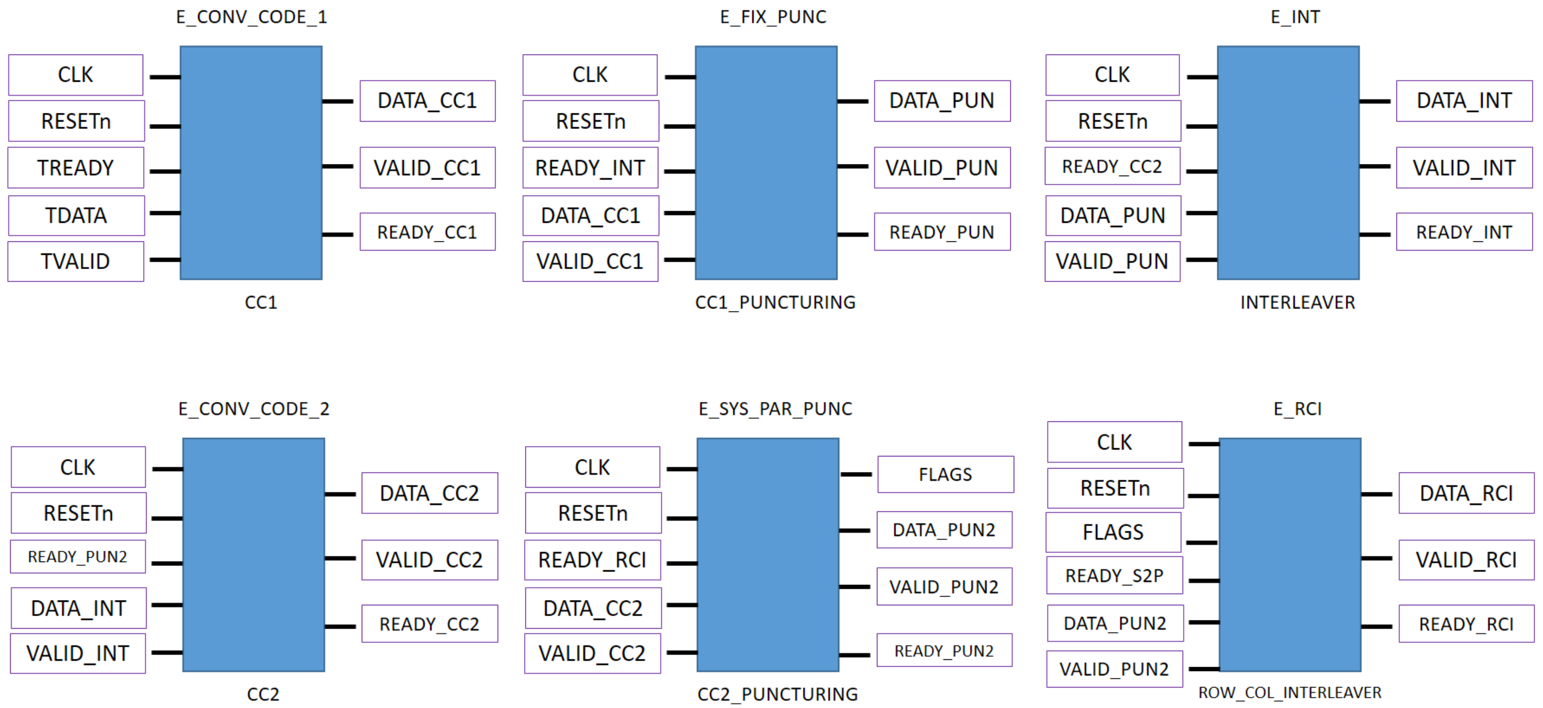
The ACM mode adaptation represents an interface for the incoming stream named “transfer frames”. The input interface maps an electrical signal to bits. The purpose of ACM is to provide the SCCC encoding unit with information blocks of varying length K with an embedded synchronization pattern that will aid the receiver to recover the binary data.
In order for the receiver to work properly, it requires that the incoming signal has sufficient bit transition density and allows the proper synchronization of the decoder. It is important to highlight that this standard is designed for high-speed data telemetry transmission, so usually large amounts of data will be transmitted. The pseudo-randomizer block diagram is shown in Figure 2. All the registers are initialized to all-ones state, then at each clock cycle, we generate a random sequence that repeats itself every 255 bits. Incoming transfer frames are randomized by XOR-ing each incoming bit with each output bit of the pseudo-randomizer. Once the transfer frame was processed, all registers must be re-initialized to the all-ones state.
A synchronization method is necessary to simplify the receiver structure and obtain sufficient performance. It is necessary that the receiver correlates the decoded binary stream with a pattern in order to find the starting index of each embedded randomized data block. Thus, a 32-bit asynchronous synchronization marker (ASM) 0x1ACFFC1D is attached at the end of each transfer frame to create a channel-data-access-unit (CADU).
Then, a stream of CADUs is fed into the slicer, whose main function is to split its continuous input into a sequence of well-defined information blocks of length K in accordance with the selected ACM format. Again, this is specified by the standard in order to simplify the implementation.
Although the ASM block seems to be simple, an efficient implementation as the one proposed in this paper is very important for the main goal of high-speed data transmission. If it is not properly designed, it will introduce several delays that can even generate problems in synchronization.

2.2. SCCC Encoding

There is a need to protect the system with a flexible coding and modulation scheme in order to adapt to different channel conditions. This capability is provided by an SCCC encoder illustrated in Figure 3. The SCCC encoder is designed as a serial turbo code that generates at its output a constant number of 8100 modulation symbols regardless of the information block size K and current ACM format. The reason for this is to allow the efficient implementation of the encoding process and thus reduce its complexity.
As in most systems, the encoder has a fixed rate and the different code rates are obtained by puncturing. CC1 is a rate 1/2 recursive, systematic convolutional code whose structure is shown in Figure 4. In this diagram, the subsequent variables appear:
  • u [ n ] denotes the n-th uncoded input bit;
  • C 1 [ n ] denotes the n-th coded systematic output bit;
  • C 2 [ n ] denotes the n-th coded parity output bit.
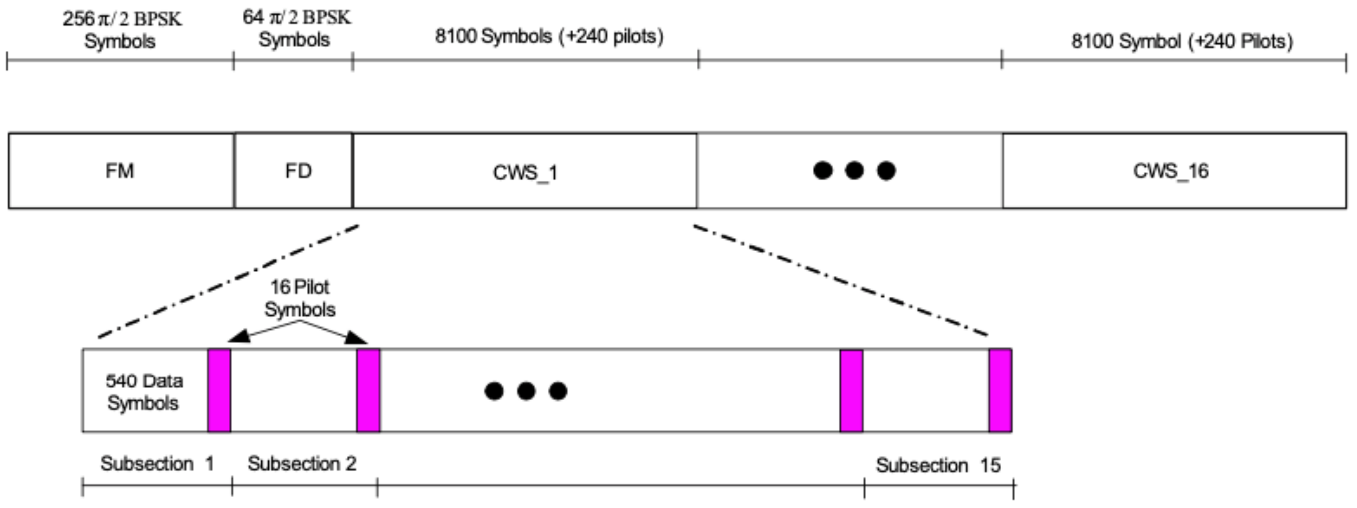
Notation follows that square brackets in u [ n ] denote the n-th vector position or equivalently the n-th clock cycle at which the operation takes place in the logical circuit. Thus, in the first clock rising edge, the input u [ 1 ] yields two output bits: the systematic bit C 1 [ 1 ] and a parity bit C 2 [ 1 ] , etc.
In summary, the convolutional encoder processes the information block of length K; when processing finishes, the switch moves into the upper position to terminate the trellis during an extra 2-bit period. Trellis termination is necessary to reset all registers to a known state, which is all-zeros by default.
To transform the CC1 1/2 rate into 2/3 rate, a fixed-puncturing scheme is used. A CC1 puncturing scheme is only fed with parity output bits from CC1 to be decimated by a factor of 1/2. Meanwhile, all systematic output bits are transmitted bits. This is better illustrated in Figure 5.
As in all the turbo codes, the interleaver is a fundamental block to construct a random code in order to spread out burst errors created by temporal fluctuations in the channel. In this standard, the interleaver implements an ad hoc permutation that could be visualized as a memory block with its size denoted by interleaver length, I. In particular, the memory block is split in such a way that it always keeps 120 rows and a variable width, such as I = 120 × W. Remember that W denotes a variable number of columns in the interleaver memory. The 120 × W memory must be written row by row, from left to right. Once the interleaver memory is filled, its content must be scrambled. For this purpose, a column bit vector with dimensions of 120 × 1 is extracted from a general column denoted by variable c. Thus, each column in the memory will be cyclically shifted by a different parameter denoted by the function β ( c ) . Now, on a second step, each column c is consistently displaced to a new column position within the memory block—a position which is different for each column and specified by the function α ( c ) . When the mixing process finishes, the memory is read row by row, from left to right. The reader may notice that there are only 19 distinct values of I, implying that only 19 unique possible permutation laws exist.
The interleaver parameters change according to the ACM format: these are W (total number of columns); α ( c ) (new column position for each column c); β ( c ) (cyclical shift for each column c). Their values are provided in tables located in [2] ANNEX B. In our implementation, several registers and shifts have been used to obtain an efficient yet reduced block. It is worth noting that this block will be made redundant in order to guarantee proper decoding, so any effort to reduce its complexity will be very useful in the future.
CC2 systematic/parity output lines are fed to two different puncturing algorithms with the aim of enabling a set of variable coding rates. The systematic puncturing algorithm uses the number of survival systematic bits, i.e., S s u r , to specify a puncturing pattern on each 300-bit sequence. The variable S represents the number of systematic bits that are divided into 300-bit sequences to puncture each sequence accordingly. After puncturing, each 300-bit sequence will contain exactly S s u r surviving bits. The parity puncturing algorithms defines a rate-matching algorithm which deletes a total number of Δ parity bits from the total stream of P parity bits. Further details of both algorithms are specified in [2].
The row/column interleaver is a block memory of size N = 8100 × m. The number of rows—8100—is the number of symbols generated from one code block; and the number of columns—m—is the modulation order which varies according to the current ACM format, as explained earlier (see the table in Figure A1). The write/read procedure is illustrated in Figure 6. When reading the row/column interleaver, each row contains m bits that modulate a symbol from the constellation mapping block.

2.3. PL Framing

The input to the PL framing processing is encoded blocks of size N. The modulation order m selects one of the possible constellations with its respective bit-mapping, as displayed in Figure 7, Figure 8, Figure 9, Figure 10 and Figure 11.
In order for the receiver to work properly, it will have to be synchronized to the RF-signal as well as perform channel and frequency offset estimation to compensate for impairments. Thus, a distributed pilot pattern is used for carrier and phase synchronization purposes. Concretely, a total of 240 pilot symbols are distributed within each block of 8100 data symbols, as represented in Figure 12. A codeword section is divided into 15 subsections, where each is composed of a 540 data symbols block and 16 pilot symbols with equal in-phase and quadrature components: I = Q = 1 2 .
Thus, PL signaling insertion creates a 320-symbol header which is divided into 256 frame marker symbols and 64 frame descriptor symbols, as shown in Figure 12. The frame marker is generated by a gold sequence which is used for the start of frame detection and synchronization. The frame descriptor is coded by a linear block code and contains information about the ACM format and pilot presence within the transmitted frame. Algorithm details for generating the frame marker and frame descriptor are defined in [2].
Physical layer pseudo-randomizer aids the telemetry link to facilitate the receiver acquisition, bit synchronization, and code synchronization. The pseudo-randomization process is applied to both data symbols and pilot symbols in the frame to prevent sending symbols in a predictive way due to pilot insertion. Frame header symbols are not randomized. The details of the randomization process are described in ANNEX C of [2].

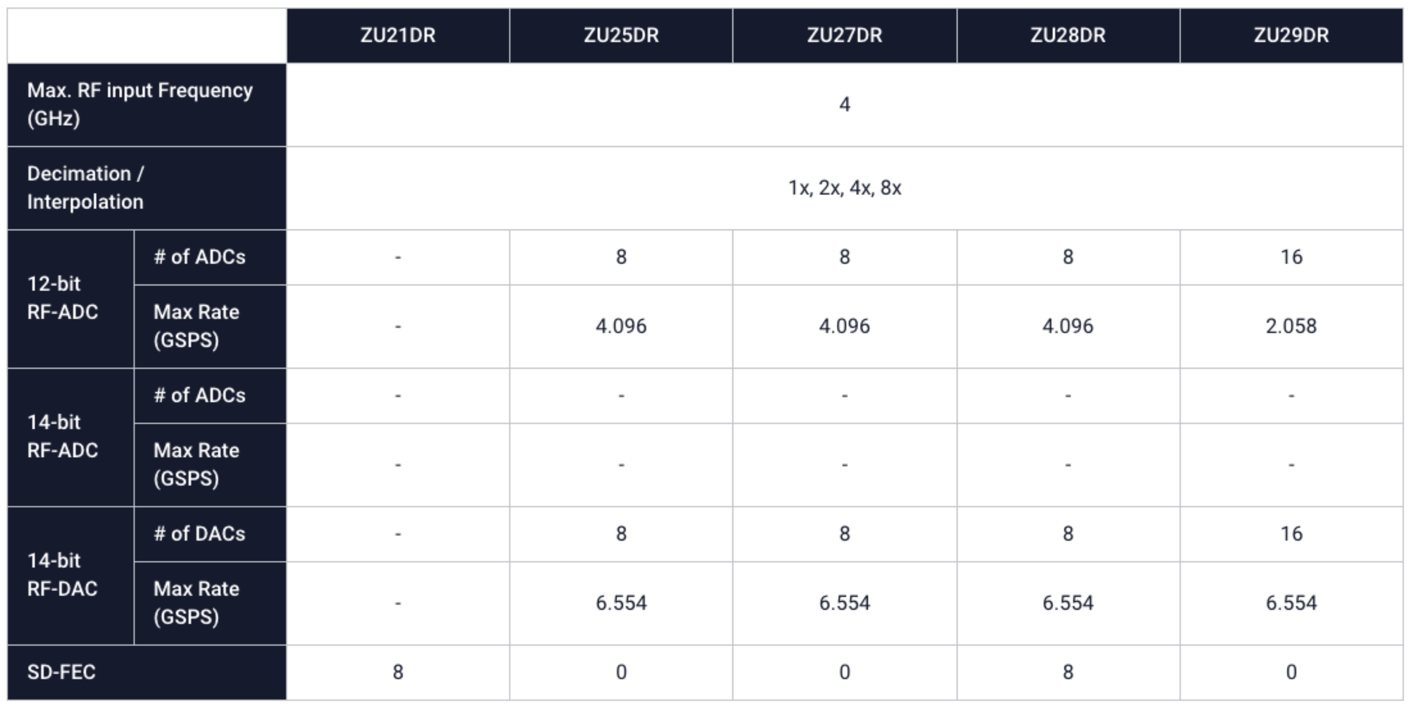
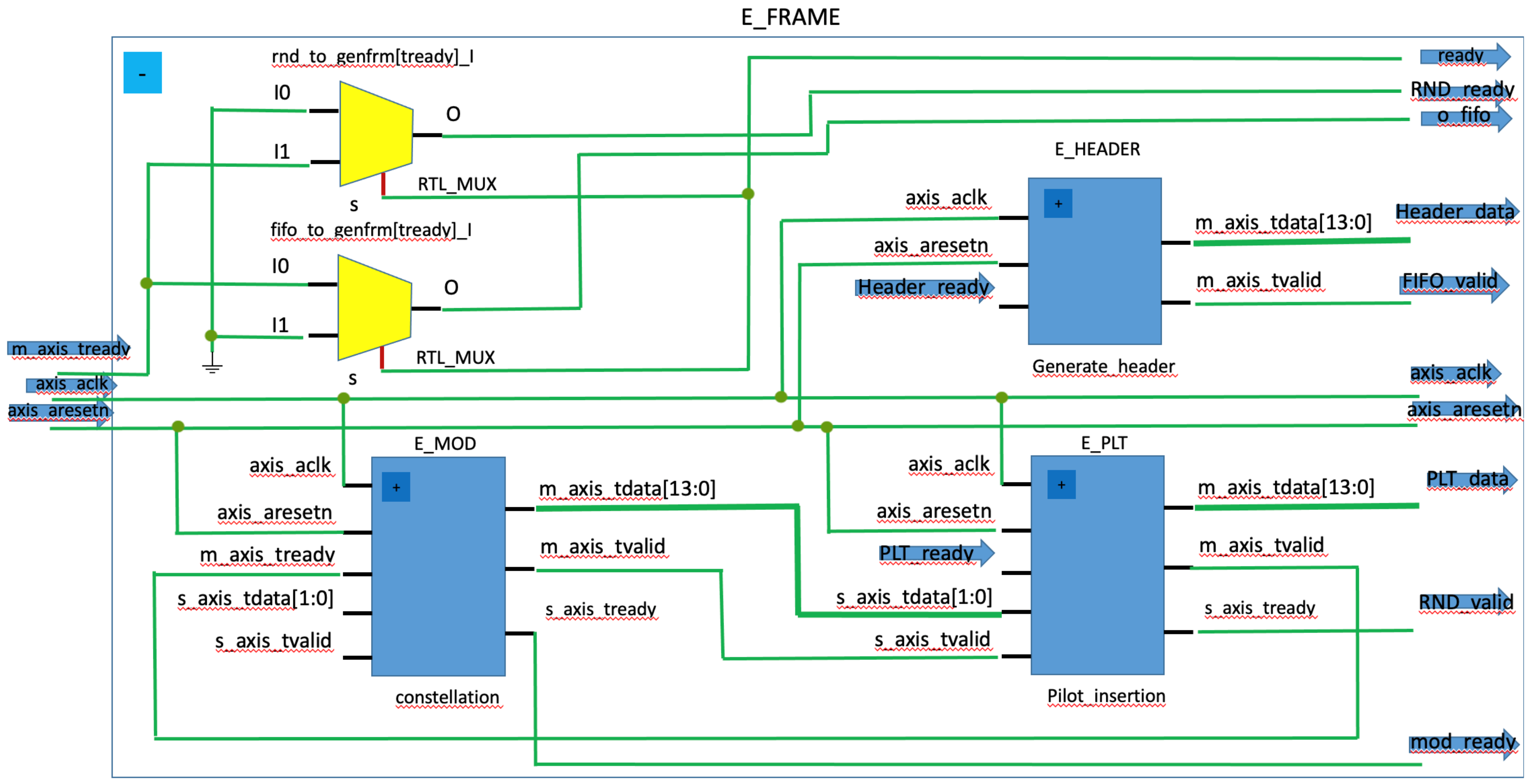
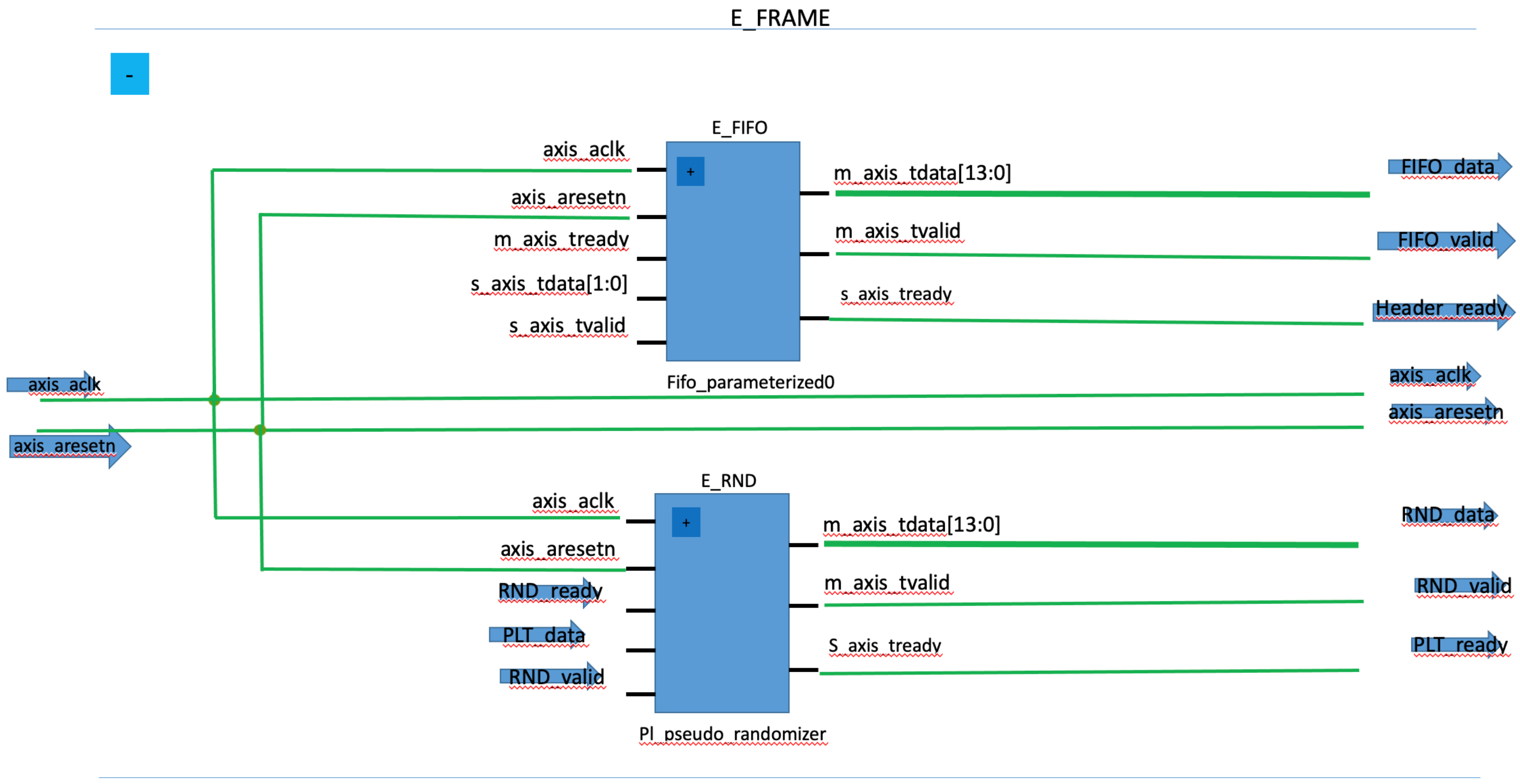
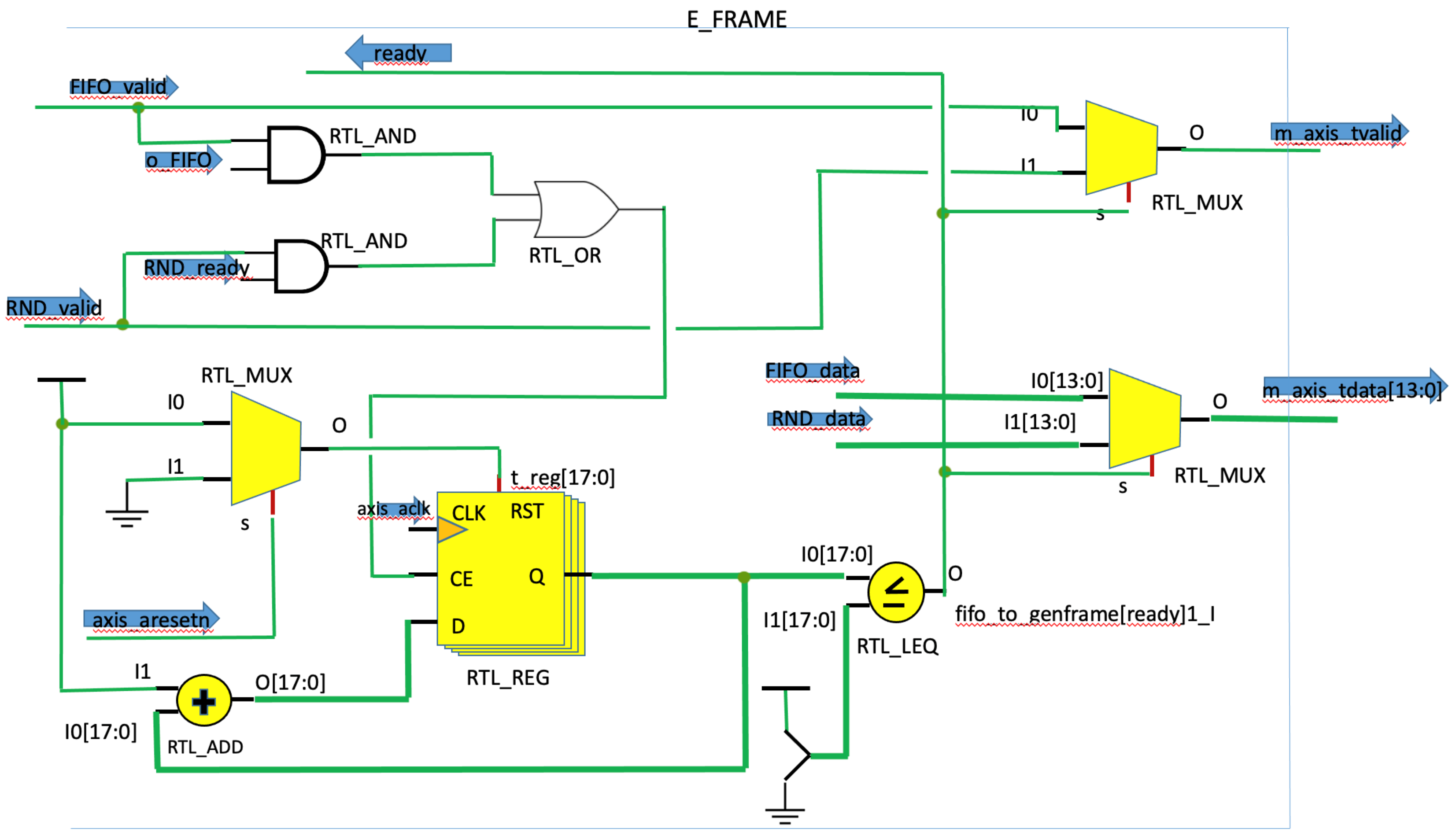
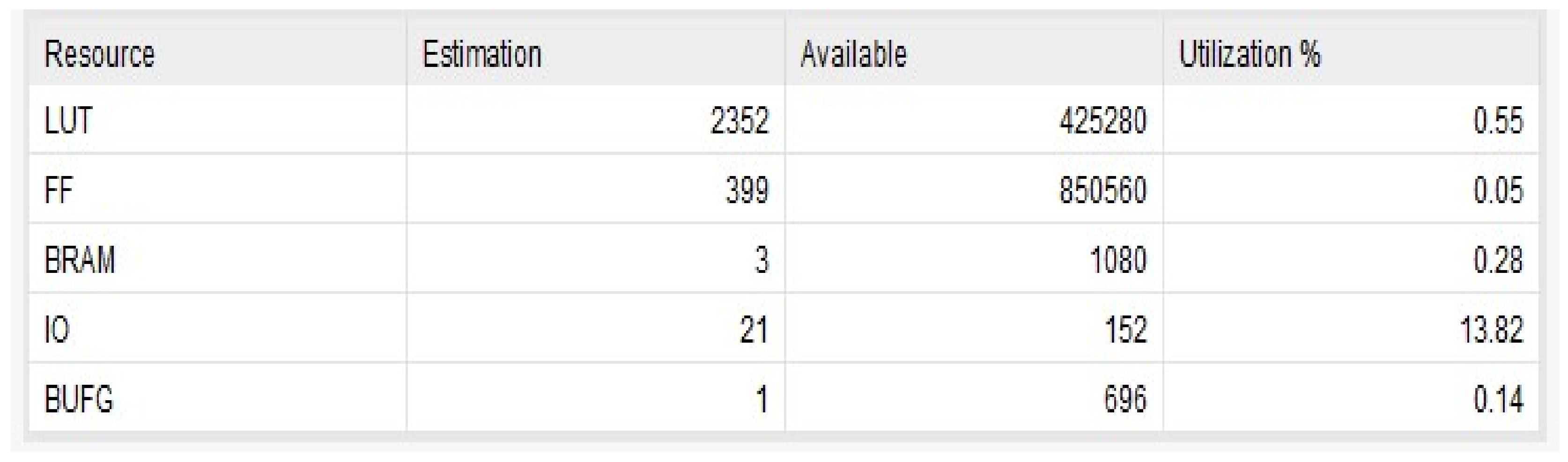
3. Flexible and Adaptive Embedded Prototype
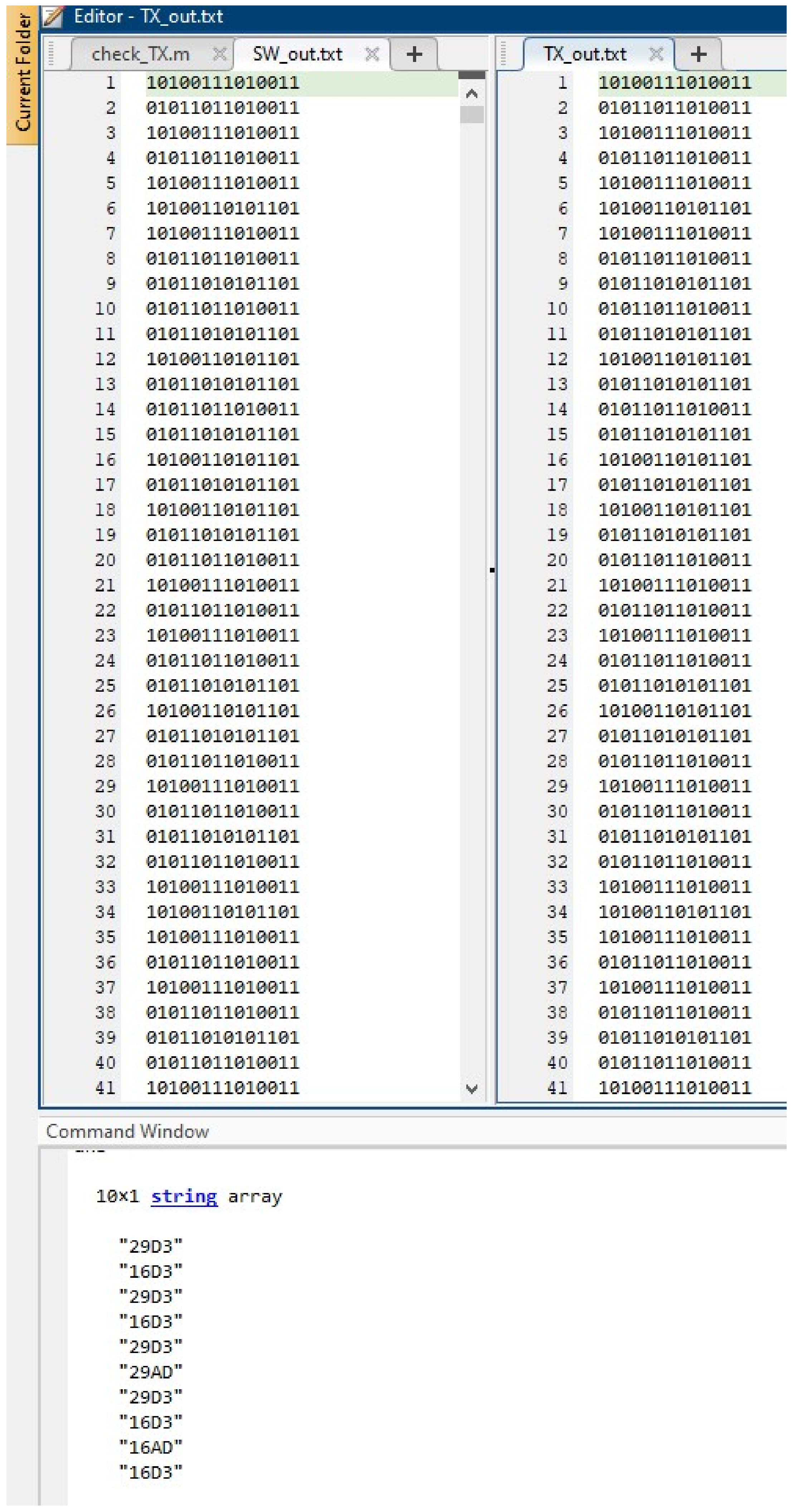
Space applications, such as satellite communications, are critical and often need to be very robust to provide radiation tolerance and high reliability. To this end, the redundancy of the main blocks is carried out. In addition, since the real-time-operating-system (RTOS) is embedded in the FPGA software, this only leave us with the FPGA fabric (logical hardware) to implement the whole data link system. Moreover, the data link is critical and highly resource demanding. As a consequence, an FPGA with enough RF-chains must be considered for this application. The Xilinx company sells a family of FPGA models called Zynq Ultrascale +RFSoC [6] whose main direct-RF chain features are shown in Figure 13.
Our choice is the model ZUDR28 since it includes soft-decision forward-error-correction (SD-FEC), which may be valuable to implement the SCCC-decoder at the receiver side.
In order to illustrate the design, several RTL schematics obtained from Vivado software are shown in Figure 14, Figure 15, Figure 16, Figure 17, Figure 18 and Figure 19. In these schematics, the reader may notice the use of AXI-stream signals [13] to interconnect the different components pairing a component’s master/output port with the slave/input port of the downstream component. Figure 15 reveals a new FIFO component in the structure. The reason is to store the output from the pseudo-randomizer while the ASM module is not ready due to the transmission of the 32-bit ASM pattern. As explained before, this is a key detail to ensure efficient implementation and prevent troublesome delays in the whole chain.
The structure of the SCCC encoding module in Figure 16 suffered slight modifications in order to accelerate the design and make it more efficient. When the inner convolutional code (CC2) outputs its systematic and parity bits in a 2-bit wide bus, this is directly fed to the SYS_PAR_PUNC unit. This is performed in order to be conservative with the AXI-stream protocol and prevent serial-parallel and parallel-serial conversions. The SYS_PAR_PUNC unit uses a finite state machine (FSM) to apply different puncturing patterns accordingly. In addition, it also provides a flag to indicate whether the output contains a systematic or parity bit, which is helpful for the row/column interleaver. Finally, an extra serial-to-parallel module is needed to transform the 1-bit stream output from the row/column interleaver into to a bus of wide m (modulation) order. It is worth nothing that the pipeline implementation allows us to optimize the data stream and obtain the maximum data rate.
The physical layer frame generation structure is a plot in Figure 17, Figure 18 and Figure 19. Considering the fact that t d a t a buses in this region must contain complex numbers, a fixed-point numeric format was employed for the real and imaginary parts, which are concatenated in the t d a t a buses. For example, if ACM format = 1, the word length is 7 bits in fixed-point data, and as a result, t d a t a buses are 14 bits wide, the first 7 bits corresponding to the real part and the following 7 bits corresponding to the imaginary part. Additionally, one must take into account that the frame header generation only needs knowledge of the current ACM format, since it does not have a slave AXI-stream port and generates the header when the reset is released. This implies that the header symbols must be saved in an FIFO until the processing propagation delay has passed, so data symbols for the PL frame start to generate. Finally, additional logic includes a counter that helps read the PL frame in the correct order, starting first with the header and later with the codeword sections, composed of data + pilot symbols. This final structure is responsible for the final maximum data rate.

4. Results

In this section, simulation results from the FPGA design are discussed.
A stimulus is necessary to test the hardware inferred in VHDL code. Using MATLAB, a contiguous random sequence of bits was stored in an input text file. Then, a testbench was coded in VHDL to read the input generated by MATLAB, apply the stimulus to the logical design, and save the output in another TXT file named “TX_out.txt”. It is important to mention that the VHDL testbench feeds the input to the transmitter using a slave AXI-stream interface and fetches the output with the help of a master AXI-stream [10]. To verify whether results are correct, one needs to have an available software-output reference stored within another TXT file named “SW_out.txt”. This is obtained by modeling the system in MATLAB. Therefore, the two TXT output files containing the software and hardware outputs are compared in Figure 20. Here, each 14-bit pattern encodes a complex symbol from the physical layer frame in fixed-point format. Since both outputs are identical, this justifies that the system is working as expected.
To further illustrate the system behavior, a snapshot of 8 usec from a timing diagram is presented in Figure 21. A timing diagram shows the transitions of all digital signals in the hardware at any time; nevertheless, in Figure 21, we only include the input/output signals of interest to the whole design. These signals are explained below.
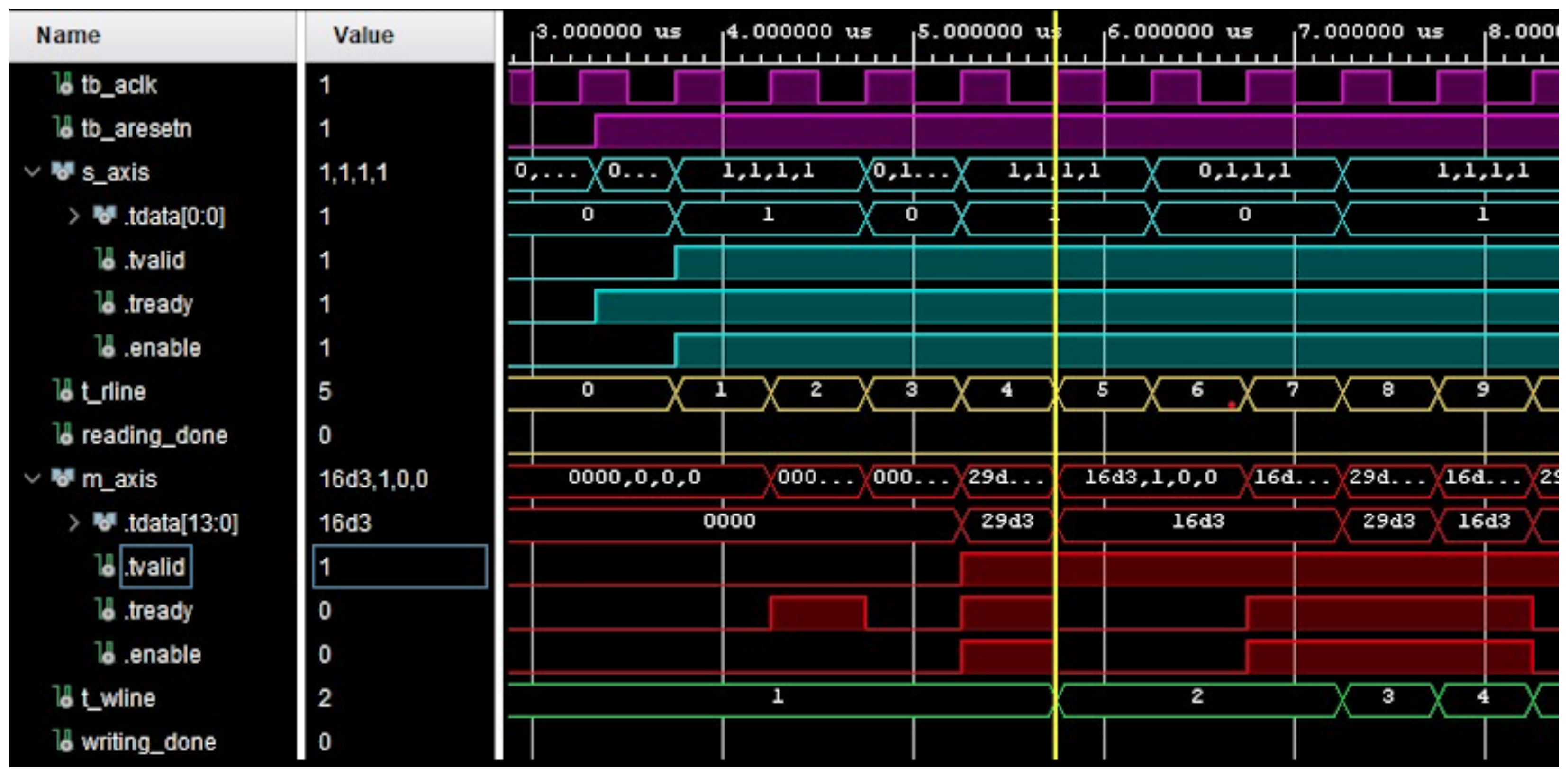
  • tb_aclk (IN) 2 MHz input clock;
  • tb_aresetn (IN) synchronous active-low reset;
  • s_axis.tdata (IN) contains input data to feed into the device.
  • s_axis.tvalid (IN) if ’1’ then the s_axis.tdata signal is considered valid;
  • s_axis.tready (OUT) is set to ’1’ when the device is ready to process the data.
  • s_axis.enable (IN) = s_axis.tvalid and s_axis.tready, signals a valid transfer of data to the device;
  • t_rline timer to count the number of lines read from the input file;
  • reading_done set to ’1’ when the input file has been read;
  • m_axis.tdata (OUT) contains output data generated by the device;
  • m_axis.tvalid (OUT) is set to ’1’ when the input data m_axis.tdata signal is considered valid;
  • m_axis.tready (IN) if ’1’, then the next device paired to the master interface is waiting to receive data;
  • m_axis.enable (OUT) = m_axis.tvalid and m_axis.tready, indicates correct data transfer through the master interface;
  • t_wline timer to count the number of lines written in output file;
  • writing_done set to ’1’ when all output data have been captured in output TXT file.
One might notice how input data in s _ a x i s . t d a t a are always valid since the transmitter is ready on every clock cycle. The signal m _ a x i s . t r e a d y is randomly generated within the testbench with the unique purpose of making the behavioral simulation more random to identify any possible bug. As stated in the AXI4-stream protocol, whenever there is a valid output datum in the master interface, i.e., m _ a x i s . t v a l i d = 1 , the control logic must not change the signal m _ a x i s . t v a l i d until the downstream component samples m _ a x i s . t d a t a . This behavior is crucial for data transfer to properly work, otherwise data could be overwritten and lost forever. This is the reason why the signal m _ a x i s . t d a t a in Figure 21 stretches over many clock cycles just until m _ a x i s . e n a b l e transitions back to ’1’. In a similar way, the counter t _ r l i n e increases whenever s _ a x i s . e n a b l e = 1 and t _ w l i n e increases when m _ a x i s . e n a b l e = 1 .
Finally, a resource utilization chart obtained by synthesis simulation is presented in Figure 22. An FPGA uses a series of building blocks to create any digital electronic circuit within itself by using configuration logic blocks. These logic blocks are the elemental building blocks of any digital system within an FGPA. Each block may contain some of the next components: look-up table (LUT), flip-flop (FF), block RAM (BRAM ), input/output pins (IO) and buffers (BUFG). Regarding Figure 22, the current transmitter design requires 21 IO lines which account for the physical layer frame output encoded by a fixed-point format employing 14 for the word length and also several control signals from the AXI-stream interfaces. Apart from this, the total use of digital components is below 1% of the total number of available components. Thus, it is safe to state that the current design is resource efficient, which is desirable since additional resources are available to allocate extra applications within the system on chip. Lastly but no less significantly, the design allows system redundancy which is crucial since backup systems are needed to fulfill the requirements of modern space communications systems in case of failure.

5. Conclusions

Throughout this paper, it was shown that an adaptive transmitter structure which meets high-performance requirements could be effectively implemented on real hardware. The possibility to use advanced re-programmable hardware was justified by the low impact on allocated hardware resources synthesized in VIVADO. It is important to mention that the standard does not specify any interconnection between the described functional modules. Then, we decided to implement AXI-stream interfaces in our model in order to optimize the serial data flow. This decision simplifies the model because the number of FIFO buffers needed is lower. Finally, the agreement between software simulations carried out by MATLAB and hardware simulations obtained from VIVADO verify the correct coding and design of the whole adaptable transmitter.
Further research can be carried out from this project. For example, timing simulations and power consumption were not analyzed. In the current study the transmitter block was synthesized, and a future study will be based on the implementation and real in-laboratory testing of the whole module. Another likely research line is the development of the receiver in the same FPGA technology, which is mandatory to enable this adaptive communication system.

Author Contributions

Conceptualization, A.L.C. and V.P.G.J.; Implementation: A.L.C.; formal analysis, A.L.C.; writing—original draft preparation, A.L.C.; writing—review and editing, V.P.G.J.; supervision, V.P.G.J. All authors have read and agreed to the published version of the manuscript.

Funding

The research was funded by Projects IRENE (PID2020-115323RB-C33) (MINECO/AEI/FEDER, UE) and MFOC (Madrid Flight on Chip—Innovation Cooperative Projects Comunidad of Madrid—HUBS 2018/Madrid Flight on Chip).

Conflicts of Interest

The authors declare no conflict of interest.

Appendix A

Figure A1. Variable managed parameters for 27 selected ACM formats.
Electronics 10 02476 g0a1

References

  1. Goldsmith, A. Wireless Communications; Cambridge University Press: Cambridge, UK, 2005. [Google Scholar]
  2. Flexible Advanced Coding and Modulation Scheme for High Rate Telemetry Applications. CCSDS 131.2-B-1. 2012. Available online: https://public.ccsds.org/Pubs/131x2b1e1.pdf (accessed on 10 August 2021).
  3. Benedetto, S.; Divsalar, D.; Montorsi, G.; Pollara, F. Serial concatenation of interleaved codes: Performance analysis, design, and iterative decoding. IEEE Trans. Inf. Theory 1998, 44, 909–926. [Google Scholar] [CrossRef]
  4. Benedetto, S.; Garello, R.; Montorsi, G.; Berrou, C.; Douillard, C.; Giancristofaro, D.; Ginesi, A.; Giugno, L.; Luise, M. MHOMS: High-speed ACM modem for satellite applications. IEEE Wirel. Commun. 2005, 12, 66–77. [Google Scholar] [CrossRef]
  5. Ugolini, A.; Montorsi, G.; Colavolpe, G. Next Generation High-Rate Telemetry. IEEE J. Sel. Areas Commun. 2018, 36, 327–337. [Google Scholar] [CrossRef]
  6. Xilinx, D. UltraScale Architecture and Product Data Sheet: Overview. Available online: https://www.xilinx.com/support/documentation/data_sheets/ds890-ultrascale-overview.pdf (accessed on 10 August 2021).
  7. Madrid Flight on Chip. 2019. Available online: https://flightonchip.es/ (accessed on 1 August 2021).
  8. Wertz, P.; Hespeler, B.; Kiessling, M.; Hagmanns, F.J. Next generation high data rate downlink subsystems based on a flexible APSK modulator applying SCCC encoding. In Proceedings of the 2016 International Workshop on Tracking, Telemetry and Command Systems for Space Applications (TTC), IEEE, Noordwijk, The Netherlands, 9–16 September 2016; pp. 1–7. [Google Scholar]
  9. Meoni, G.; Cassettari, R.; Bertolucci, M.; Marino, A.; Davalle, D.; Trafeli, M.; Fanucci, L. CCSDS 131.2-B-1 telemetry transmitter: A VHDL IP core and a validation architecture on board RTG4 FPGA. Acta Astronaut. 2020, 176, 484–493. [Google Scholar] [CrossRef]
  10. ARM. AMBA AXI-Stream Protocol Specification. Available online: https://developer.arm.com/documentation/ihi0051/latest (accessed on 2 August 2021).
  11. Louliej, A.; Jabrane, Y.; Jiménez, V.P.G.; Guilloud, F. Dimensioning an FPGA for Real-Time Implementation of State of the Art Neural Network-Based HPA Predistorter. Electronics 2021, 10, 1538. [Google Scholar] [CrossRef]
  12. Louliej, A.; Jabrane, Y.; Gil Jiménez, V.P.; García Armada, A. Practical Guidelines for Approaching the Implementation of Neural Networks on FPGA for PAPR Reduction in Vehicular Networks. Sensors 2019, 19, 116. [Google Scholar] [CrossRef] [PubMed] [Green Version]
  13. Caba, J.; Rincón, F.; Barba, J.; de la Torre, J.A.; López, J.C. FPGA-Based Solution for On-Board Verification of Hardware Modules Using HLS. Electronics 2020, 9, 2024. [Google Scholar] [CrossRef]
Figure 1. Functional block diagram.
Electronics 10 02476 g001
Figure 2. Pseudo-randomizer architecture.
Electronics 10 02476 g002
Figure 3. Serial turbo code architecture.
Electronics 10 02476 g003
Figure 4. Convolutional code block diagram for CC1 and CC2.
Electronics 10 02476 g004
Figure 5. CC1 parity decimation puncturing scheme.
Electronics 10 02476 g005
Figure 6. Bit-interleaving scheme.
Electronics 10 02476 g006
Figure 7. QPSK.
Figure 7. QPSK.
Electronics 10 02476 g007
Figure 8. 8-PSK.
Figure 8. 8-PSK.
Electronics 10 02476 g008
Figure 9. 16-APSK.
Figure 9. 16-APSK.
Electronics 10 02476 g009
Figure 10. 32-APSK.
Figure 10. 32-APSK.
Electronics 10 02476 g010
Figure 11. 64-APSK.
Figure 11. 64-APSK.
Electronics 10 02476 g011
Figure 12. Physical layer frame structure.
Electronics 10 02476 g012
Figure 13. RFSoC features’ comparison table.
Electronics 10 02476 g013
Figure 14. Transmitter RTL block diagram.
Electronics 10 02476 g014
Figure 15. ACM mode adaptation RTL block diagram.
Electronics 10 02476 g015
Figure 16. SCCC encoder block diagram. The S2P block is serial to the parallel block.
Electronics 10 02476 g016
Figure 17. Part I—physical layer frame RTL block diagram.
Electronics 10 02476 g017
Figure 18. PART II—physical layer frame RTL block diagram.
Electronics 10 02476 g018
Figure 19. PART III—physical layer frame RTL block diagram.
Electronics 10 02476 g019
Figure 20. MATLAB output for the first 41 symbols of a PL frame.
Electronics 10 02476 g020
Figure 21. Timing diagram for the first 8 output bits after initialization.
Electronics 10 02476 g021
Figure 22. Resources used in the implementation.
Electronics 10 02476 g022
Publisher’s Note: MDPI stays neutral with regard to jurisdictional claims in published maps and institutional affiliations.

