Abstract
A high-speed programmable frequency divider for a Ka-band phase-locked loop (PLL)-type frequency synthesizer system is presented and fabricated in 90 nm CMOS technology. It consists mainly of a divided-by-8/9 dual-modulus prescaler (DMP) and pulse swallow counters. An active-inductor-based source-coupled logic (SCL) D flip-flop (DFF) and the “OR” gate are used in the DMP in order to promote its locking range and operation frequency. The measured operation frequency range of the improved programmable frequency divider covers from 6 to 20 GHz with a low phase noise of less than −136 dBc/Hz at a 1 MHz offset of output signals, an optimum sensitivity of −27 dBm at 15 GHz, and a low power consumption of 9.1 mW.
1. Introduction
Phase-locked loop (PLL)-type frequency synthesizers are widely used to generate local frequency signals in RF transceivers. Programmable frequency dividers are indispensable in PLL-type frequency synthesizers [1,2,3]. Important specifications, such as a wide operation frequency range, low phase noise, and low power consumption are significant to programmable frequency dividers [4,5,6].
Frequency dividers on the basis of a fixed-modulus divider chain are introduced to frequency synthesizers to achieve a higher operating frequency and a wider frequency range. Nevertheless, the frequency divider is not able to work with any different frequency division ratio because the frequency division ratio is fixed by the PLL system in this case [7,8,9]. The programmable frequency dividers on the foundation of a chain of n divide-by-2/3 cells are the additional methods utilized to obtain a higher operating frequency and a wider operation frequency range. However, division ratios lower than 2n cannot be obtained in this topology [10]. Furthermore, higher power consumption will be consumed in the divide-by-2/3-cells-based programmable frequency divider when the current-mode logic (CML)-based latches are employed in the D flip-flop (DFF) of divide-by-2/3 cells [11]. Hence, a suitable, programmable frequency divider based on a dual-modulus prescaler (DMP) and pulse swallow (PS) counters with a higher operating frequency and a wider operation frequency range seems particularly advantageous [12,13].
This paper presents an improved programmable frequency divider for a Ka-band PLL-type frequency synthesizer in a 90 nm CMOS process. An active-inductor-based source-coupled logic (SCL) DFF topology is used in the synchronous divided-by-4/5 circuit of the programmable frequency divider to promote its locking range and operation frequency. Experimental results demonstrate expected properties of proposed circuits. Compared to conventional frequency dividers with a fixed frequency division and the other high-speed frequency divider with higher power consumption, the improved programmable frequency divider shows features such as a higher operating frequency, a wider operation frequency range, a more variable frequency division ratio, and lower power consumption. The key circuit techniques are discussed in Section 2. The experimental results are exhibited and summarized in Section 3. At last, some conclusions are given in Section 4.
2. Circuit Design
The architecture of the Ka-band PLL-type frequency synthesizer system containing the programmable frequency dividers based on pulse swallow counter topology is shown in Figure 1, where the programmable frequency dividers consist of a divide-by-N/N + 1 DMP and pulse swallow (PS) counters made up of a pulse counter of counter-P and a swallow counter of counter-S. Some active-inductor-based SCL DFF topologies are used in the synchronous divided-by-4/5 circuit of the DMP to promote the locking range and operation frequency.
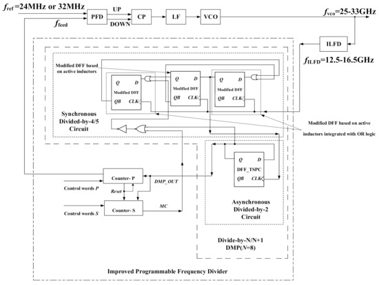
Figure 1.
Block diagram of the Ka-band PLL and the improved programmable frequency divider.
As denoted in Figure 2, the values of P and S are set to counter-P and counter-S, respectively, when they begin to count. The DMP divides the high frequency input signal by N + 1 until counter-S counts up to S. At this point, it switches over and starts to divide-by N until counter-P counts up to P. Then, two counters will be reset and the DMP will switch back to divide by N + 1 simultaneously [14,15]. The total division ratio of the downscaling circuit is:
M = (N + 1)S + N(P − S) = NP + S,

Figure 2.
Working principle illustration for the frequency division ratio of the improved programmable frequency divider.
Figure 1 shows that the frequency range of the output signal of the VCO is from 25 GHz to 33 GHz, and therefore that of the injection-locked frequency divider (ILFD) is from 12.5 to 16.5 GHz in the Ka-band PLL. As the circuit of the following stage of the ILFD, the operation frequency range of the programmable frequency divider in the Ka-band PLL should cover the frequency range of the ILFD’s output signal [2,9]. Because there are two optional reference frequency sources of 24 MHz and 32 MHz for the Ka-band PLL, the corresponding variation ranges of the frequency division ratio, M, of the proposed programmable frequency divider are 250–688 and 390–516, respectively. Considering the versatility and portability of the proposed circuit, the improved programmable frequency divider achieves a frequency range from 6 to 20 GHz. Consequently, the value of n is 8, the numerical variation range of M is 250–700, the numerical variation range of P is 30–87, and the numerical variation range of S is 0–7.
2.1. Dual-Modulus Prescaler
As revealed in Figure 1, the divide-by-8/9 DMP consists mainly of a synchronous divided-by-4/5 circuit and an asynchronous divided-by-2 circuit.
Since the synchronous divided-by-4/5 circuit works at the highest frequency in the divide-by-8/9 DMP, it should have features such as a wider operation frequency range, higher speed, lower consumption, and lower phase noise [16]. To promote the locking range and operation frequency, some techniques are adopted to optimize the circuit’s performance.
As revealed in Figure 3, the active inductors realized by transistors M1–M4 and M11–M14 are merged to extend the bandwidth of the latch in the source-coupled logic (SCL) DFFs and then increase the operation frequency of the synchronous divided-by-4/5 circuit. As shown in Figure 4, OR gates are also integrated into DFFs to restrain additional gate delays.
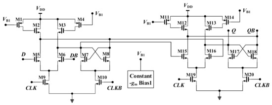
Figure 3.
Schematic of the modified DFF based on active inductors.
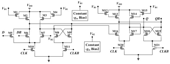
Figure 4.
Schematic of the modified DFF based on active inductors integrated with “OR” logic.
The active inductor’s impedance can be expressed as [17]:
where R means the controllable resistor realized by transistors M1 (M11) and M4 (M14); gm represents the transconductance parasitic gate–source capacitance of transistors M2 (M12) and M3 (M13); and Cgs denotes the parasitic gate–source capacitance of these transistors. The active inductor can be regarded as an inductor, Ls, in series with a resistor, Rs. The inductance of the active inductor can eliminate the effects of the M2 (M12) and M3 (M13) transistors’ parasitic gate–source capacitances. Therefore, the operating frequency and bandwidth of the latches will be promoted.
Z ≈ Rs + Ls·s = 1/gm + (Cgs·R/gm) · s,
A reasonable value of Ls is also related to the involved bias voltage. As exhibited in Figure 3 and Figure 4, constant-gm bias circuits are used in the DFFs mentioned above to generate bias voltage. In contrast to the bias voltage based on a network of resistors, constant-gm bias circuits are able to provide more stable output voltages [18,19].
It is shown in Figure 5 that the asynchronous divided-by-2 circuit in the DMP is implemented with true single-phase-clocked (TSPC) DFFs to achieve higher input sensitivity and lower power consumption.
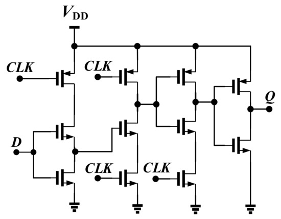
Figure 5.
Schematic diagram of a TSPC DFF (DFF1) for an asynchronous divider.
Figure 6 shows the simulated input sensitivity curves of the proposed programmable frequency divider and its counterpart without active-inductor-based SCL DFFs. Obviously, the proposed programmable frequency divider has a larger operation frequency range and a better input sensitivity character than the counterpart without active inductors. The active-inductor-based SCL DFFs promote the locking range and operation frequency of the programmable frequency divider effectively.
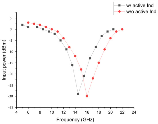
Figure 6.
Simulated input sensitivity curves with and without active-inductor-based SCL DFFs.
Figure 7 exhibits a comparison of simulated time delay between the asynchronous divide-by-2 circuit based on the TSPC DFF shown in Figure 5 and its counterpart based on a conventional transmission gate DFF. As presented in Figure 7, the TSPC-DFF-based asynchronous divider is more suitable for the improved programmable frequency divider since the TSPC-DFF-based asynchronous divider has a smaller time delay than the conventional transmission-gate-DFF-based asynchronous divider.
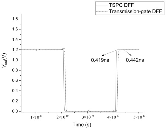
Figure 7.
Simulated time delay of asynchronous divide-by-2 circuits based on different kinds of DFFs.
2.2. Pulse Swallow Counters
The block diagram of the PS counters is presented in Figure 8a. The working principle of the swallow counter is roughly the same as that of the pulse counter. Either of the two subtractor-based counters will reset and restart counting again if they reduce to 0 [20]. Transistor-level implementation of the TSPC DFFs in the PS counters is illustrated in Figure 8b,c. Some logic gates are embedded into the TSPC DFFs to make them adapt to a higher operation frequency.
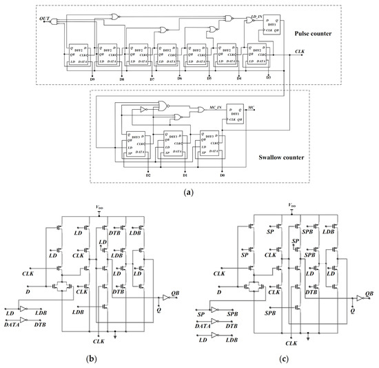
Figure 8.
Diagrams: (a) block diagram of the PS counters; (b) schematic diagram of DFF2 in counter-P; and (c) schematic diagram of DFF3 in counter-S.
3. Experimental Results
The improved programmable frequency divider was fabricated in 90 nm CMOS technology with a 1.2 V power supply, with a die area of 0.165 mm2 including the pads. The microphotograph of the programmable frequency divider chip is shown in Figure 9.
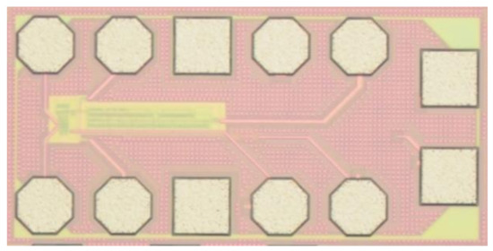
Figure 9.
Chip microphotograph of the programmable frequency divider.
Figure 10a demonstrates the measured, improved programmable frequency divider’s output waveform of 18.52 MHz with an input signal of 12 GHz when the total frequency division ratio is set as 648. The measured output voltage swing (VPk-Pk) on an external 50 Ω load is about 450 mV. Meanwhile, Figure 10b shows the measured, improved programmable frequency divider’s output waveform of 32.32 MHz with an input signal of 19 GHz when the total frequency division ratio is set as 588. The measured output VPk-Pk on an external 50 Ω load is about 380 mV. It can be seen from the experimental results exhibited in Figure 10 that the operation frequency range of the improved programmable frequency divider covers the frequency range of the output signal of the ILFD in the Ka-band PLL. Figure 11 reveals the measured phase noises at a 1 MHz offset of output signals of the programmable frequency divider at different input signals and division rates kept at a low level of less than −136 dBc/Hz. Figure 12 indicates that the measured input sensitivity of the programmable frequency divider is very high, given that the minimum input power is only −27 dBm at 15 GHz.
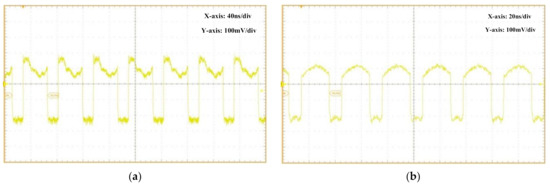
Figure 10.
Measured output waveforms of the improved programmable frequency divider: (a) fin = 12 GHz, n = 648; (b) fin = 19 GHz, n = 588.
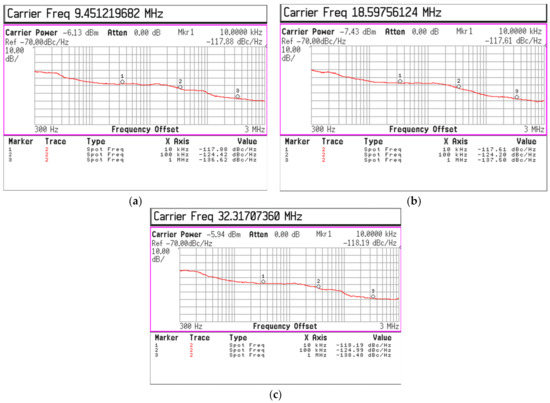
Figure 11.
Measured phase noise of the improved programmable integer divider’s output signal: (a) fin = 6.2 GHz, n = 656, and fout = 9.452 MHz; (b) fin = 11.3 GHz, n = 608, and fout = 18.597 MHz; and (c) fin = 19 GHz, n = 588, and fout = 32.32 MHz.
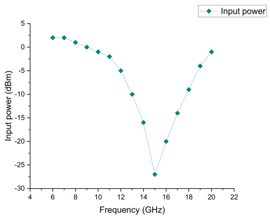
Figure 12.
Measured simulated input sensitivity curves of the programmable frequency divider.
The experimental results above verify the active-inductor-based SCL DFFs can promote the operation frequency range of the programmable frequency divider effectively. Table 1 compares the performance of the improved programmable frequency divider to some other prior published scientific papers. It can be seen that the improved programmable frequency divider attains a wider operation frequency range with lower power consumption and lower phase noise.

Table 1.
Performance summary and comparison to other works.
4. Conclusions
An improved programmable frequency divider is fabricated in a 90 nm CMOS technology. An active-inductor-based SCL DFF topology is introduced to the synchronous divided-by-4/5 circuit of the programmable frequency divider to promote the operation frequency range and operation frequency. The chip area of the programmable frequency divider is 0.165 mm2. The operation frequency range of the improved programmable frequency divider covers from 6 to 20 GHz with a low power consumption of 9.1 mW. All the phase noises at a 1 MHz offset of output signals of the programmable frequency divider at different input signals and division rates were kept at a low level of less than −136 dBc/Hz. The input sensitivity of the programmable frequency divider is as low as −27 dBm at 15 GHz. Experimental results demonstrate that the improved programmable frequency divider is suitable for Ka-band PLL applications in an RF receiver system.
Author Contributions
Conceptualization and methodology, L.T. and K.C.; writing—original draft preparation, L.T. and K.C.; writing—review and editing, L.T. and Y.Z.; visualization, L.T.; supervision, X.T.; project administration, L.T.; funding acquisition, L.T., C.Z. and X.T. All authors have read and agreed to the published version of the manuscript.
Funding
This work is supported by the National Natural Science Foundation of China (No. 61674036 and 61774037) and the National Key Research and Development Program of China (No. 2018YFB2202200).
Conflicts of Interest
The authors declare no conflict of interest.
References
- Wang, J.; Wang, Z.; Xu, J.; Wu, Y.; Tian, M.; Lei, X.; Ma, L.; Tang, L. A multi-band CMOS PLL-based frequency synthesizer for DRM/DRM+/DAB systems. Analog Integr. Circuits Signal Process. 2014, 80, 293–304. [Google Scholar] [CrossRef]
- Huang, Z.; Luong, H.C. An 82–107.6-GHz Integer-N ADPLL Employing a DCO with Split Transformer and Dual-Path Switched-Capacitor Ladder and a Clock-Skew-Sampling Delta–Sigma TDC. IEEE J. Solid-State Circuit 2019, 54, 358–367. [Google Scholar] [CrossRef]
- Huang, S.; Liu, S.; Hu, J.; Wang, R.; Zhu, Z. A 12-GHz Wideband Fractional-N PLL with Robust VCO in 65-nm CMOS. IEEE Microw. Wirel. Compon. Lett. 2019, 29, 397–399. [Google Scholar] [CrossRef]
- Delden, M.v.; Pohl, N.; Aufinger, K.; Musch, T. A 94 GHz programmable frequency divider with inductive peaking for wideband and highly stable frequency synthesizers. In Proceedings of the 2017 12th European Microwave Integrated Circuits Conference (EuMIC), Nuremberg, Germany, 8–10 October 2017; pp. 9–12. [Google Scholar]
- Issakov, V.; Trotta, S. Low-power dual-modulus frequency divider by 4/5 up to 13-GHz in 0.13 μm CMOS. In Proceedings of the 2017 IEEE International Conference on Microwaves, Antennas, Communications and Electronic Systems (COMCAS), Tel-Aviv, Israel, 13–15 November 2017; pp. 1–4. [Google Scholar]
- Purohit, S.; Nirmal, U. A Novel 8.4 GHz, High Speed and Low Power Design of Programmable Divider in 180nm CMOS Technology. In Proceedings of the 2019 2nd International Conference on Intelligent Communication and Computational Techniques (ICCT), Jaipur, India, 28–29 September 2019; pp. 192–195. [Google Scholar]
- Wu, W.; Staszewski, R.B.; Long, J.R. A 56.4-to-63.4 GHz Multi-Rate All-Digital Fractional-N PLL for FMCW Radar Applications in 65 nm CMOS. IEEE J. Solid-State Circuit 2014, 49, 1081–1096. [Google Scholar] [CrossRef]
- Hussein, A.I.; Vasadi, S.; Paramesh, J. A 50–66-GHz Phase-Domain Digital Frequency Synthesizer with Low Phase Noise and Low Fractional Spurs. IEEE J. Solid-State Circuit 2017, 52, 3329–3347. [Google Scholar] [CrossRef]
- Abedi, R.; Kananizadeh, R.; Momeni, O.; Heydari, P. A CMOS V-Band PLL with a Harmonic Positive Feedback VCO Leveraging Operation in Triode Region for Phase-Noise Improvement. IEEE Trans. Circuits Syst. I-Regul. Pap. 2019, 66, 1818–1830. [Google Scholar] [CrossRef]
- Vaucher, C.S.; Ferencic, I.; Locher, M.; Sedvallson, S.; Voegeli, U.; Wang, Z. A family of low-power truly modular programmable dividers in standard 0.35-μm CMOS technology. IEEE J. Solid-State Circuit 2000, 35, 1039–1045. [Google Scholar] [CrossRef]
- Jin, J.; Liu, X.; Mo, T.; Zhou, J. Quantization Noise Suppression in Fractional-N PLLs Utilizing Glitch-Free Phase Switching Multi-Modulus Frequency Divider. IEEE Trans. Circuits Syst. I-Regul. Pap. 2012, 59, 926–937. [Google Scholar] [CrossRef]
- Ping-Yuan, D.; Jean-Fu, K. A 5-GHz CMOS Frequency Synthesizer with an Injection-Locked Frequency Divider and Differential Switched Capacitors. IEEE Trans. Circuits Syst. I-Regul. Pap. 2009, 56, 320–326. [Google Scholar] [CrossRef]
- Fan, X.; Tang, L.; Wang, Y.; Yu, L.; Yuan, L.; Yang, Z.; Wang, Z. A 1 V 0.18 μm fully integrated integer-N frequency synthesizer for 2.4 GHz wireless sensor network applications. Analog Integr. Circuits Signal Process. 2014, 82, 251–264. [Google Scholar] [CrossRef]
- Shin, J.; Shin, H. A 1.9–3.8 GHz ΔΣ Fractional-N PLL Frequency Synthesizer with Fast Auto-Calibration of Loop Bandwidth and VCO Frequency. IEEE J. Solid-State Circuit 2012, 47, 665–675. [Google Scholar] [CrossRef]
- Hati, M.K.; Bhattacharyya, T.K. A novel pulse swallow based frequency divider circuit for a phase-locked loops. Analog Integr. Circuits Signal Process. 2017, 92, 55–69. [Google Scholar] [CrossRef]
- Haiyong, S.; Zhiqun, L. A 5-GHz programmable frequency divider in 0.18-μm CMOS technology. J. Semicond. 2010, 31, 055004. [Google Scholar] [CrossRef]
- Zhang, C.; Wang, X.; Fang, J.; Zhang, Y.; Tang, L. A CMOS fully differential ring VCO with active inductors and I/Q outputs. Microw. Opt. Technol. Lett. 2018, 61, 937–942. [Google Scholar] [CrossRef]
- Shen, Y.; Zhang, R. Constant-gm Bias Circuit without Off-Chip Components. In Proceedings of the 13th IEEE International Conference on Solid-State and Integrated Circuit Technology (ICSICT), Hangzhou, China, 25–28 October 2016; pp. 1309–1311. [Google Scholar]
- Talebbeydokhti, N.; Hanumolu, P.K.; Kurahashi, P.; Un-Ku, M. Constant transconductance bias circuit with an on-chip resistor. In Proceedings of the 2006 IEEE International Symposium on Circuits and Systems, Kos, Greece, 21–24 May 2006; pp. 2857–2860. [Google Scholar]
- Zhiqiang, G.; Yuanxu, X.; Peng, S.; Enyi, Y.; Yongshuang, H. A programmable high-speed pulse swallow divide-by-N frequency divider for PLL frequency synthesizer. In Proceedings of the 2010 International Conference on Computer Application and System Modeling (ICCASM 2010), Taiyuan, China, 22–24 October 2010; pp. V6-315–V6-318. [Google Scholar]
- Gu, Q.J.; Gao, Z. A CMOS High Speed Multi-Modulus Divider With Retiming for Jitter Suppression. IEEE Microw. Wirel. Compon. Lett. 2013, 23, 554–556. [Google Scholar] [CrossRef]
- Ergintav, A.; Herzel, F.; Borngraeber, J.; Ng, H.J.; Kissinger, D. Low-power and low-noise programmable frequency dividers in a 130 nm SiGe BiCMOS technology. In Proceedings of the 2017 15th IEEE International New Circuits and Systems Conference (NEWCAS), Strasbourg, France, 25–28 June 2017; pp. 105–108. [Google Scholar]
- Lin, Y.; Huang, W.; Lu, C.; Wang, Y. Wide-Locking-Range Multi-Phase-Outputs Regenerative Frequency Dividers Using Even-Harmonic Mixers and CML Loop Dividers. IEEE Trans. Microw. Theory Tech. 2014, 62, 3065–3075. [Google Scholar] [CrossRef]
- Wang, Y.; Wang, Y.; Wu, Z.; Quan, Z.; Liou, J.J. A Programmable Frequency Divider with a Full Modulus Range and 50% Output Duty Cycle. IEEE Access 2020, 8, 102032–102039. [Google Scholar] [CrossRef]
- Kim, N.; Rabaey, J.M. A 3–10mW, 3.1–10.6GHz integer-N QPLL with reference spur reduction technique for UWB-based cognitive radios. In Proceedings of the 2015 IEEE Radio Frequency Integrated Circuits Symposium (RFIC), Phoenix, AZ, USA, 17–19 May 2015; pp. 67–70. [Google Scholar]
Publisher’s Note: MDPI stays neutral with regard to jurisdictional claims in published maps and institutional affiliations. |
© 2021 by the authors. Licensee MDPI, Basel, Switzerland. This article is an open access article distributed under the terms and conditions of the Creative Commons Attribution (CC BY) license (https://creativecommons.org/licenses/by/4.0/).


