Abstract
The second-harmonic input impedance plays a critical role on the performance of GaN power amplifiers. In a recent paper, a drain efficiency enhancement for a continuous-mode power amplifiers was reported to be achieved using active broadband second-harmonic injection at the PA input. In this paper, the strategy for selecting the second-harmonic input impedance and the necessity for using active injection in such broadband PAs are discussed in detail. Additionally, the methodology for designing an embedded broadband diplexer in the input matching network is reported. Finally, the importance of the phase of the second-harmonic signal injected is demonstrated for both CW and modulated signals using both simulation and measurement, respectively. The effectiveness of the CW and modulated active second-harmonic injection methodology presented here are validated by previously reported measurements that demonstrated an average drain efficiency improvement of 9.4% from 1.3 to 2.4 GHz for CW signals and of 9.7% at 2 GHz for a frequency-modulated 30 MHz chirp radar signal.
1. Introduction
There is growing interest in realizing highly efficient power amplifiers (PA) for radar applications using GaN technology. Benefiting from its high mobility and high breakdown voltage, compound material-based Gallium Nitride (GaN) PAs offer promising opportunities for realizing high-performance radar systems. For radar applications, high-efficiency broadband PAs are needed. Waveform-engineering based continuous mode PAs, such as class J [1,2], clockwise-loaded class-J (CLCJ) [3], continuous class F [4,5], and class F [6,7], have been studied extensively for broadening the operating bandwidth. The majority of continuous mode research focused more on the waveform engineering at the drain current source reference plane (CSRF). On the other side, the input second-harmonic source impedance has not attracted much attention from an efficiency perspective.
Recently, various studies have drawn attention to the correlation between the input second-harmonic source impedance and the drain efficiency especially for GaN-based PAs [8,9,10,11,12,13]. The load-pull based analyses in these references have demonstrated that the drain efficiency is sensitive to not only the load impedance but also the source impedance . For a given output matching network (OMN), which places the second-harmonic load impedance close to a short (e.g., class-J, continuous class-F, or CLCJ), an efficiency-extrema region can be observed along the edge of the Smith Chart for the input second-harmonic impedance . The gate to source capacitance (Cgs) is shown in [9] to induce an input voltage distortion that explains this behavior. Operating the PA in the minimum-efficiency region of can cause a drastic drain efficiency drop due to the distorted intrinsic loadline. It is also found that the maximum-efficiency and minimum-efficiency regions of are usually adjacent. As a consequence, it is challenging to design the input matching network (IMN) such that approach the maximum-efficiency region while avoiding the adjacent minimum-efficiency region as the frequency varies. Hence, an extremely precise agreement between the simulation and measurement is then required for IMN design. When it comes to broadband IMN design, however, the discrepancy between the simulation and measurement is often more obvious due to the use of high-order filters to simultaneously control the fundamental and second-harmonic impedances. Furthermore, the ideal trajectory for maximum efficiency is often non-Foster, which poses even more challenges to broadband IMN design.
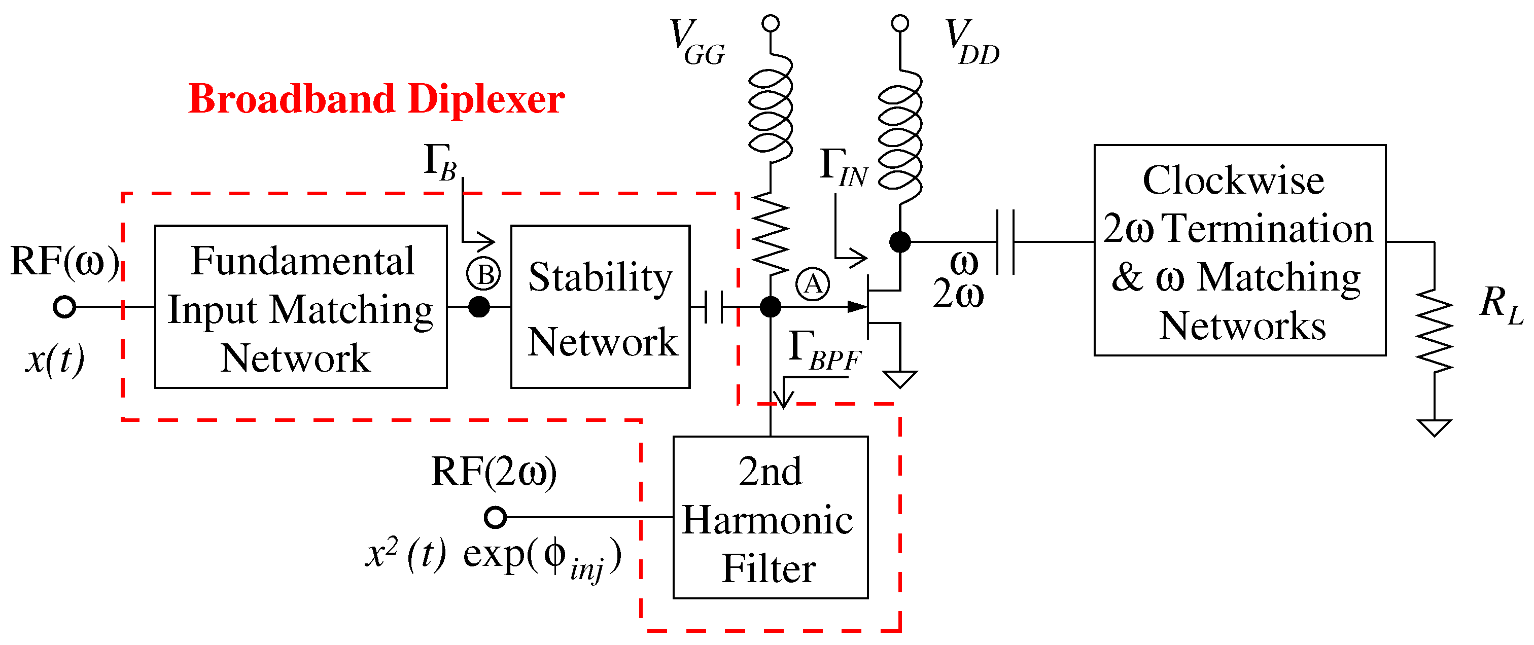
In this paper, an assisted input second-harmonic injection allows the designer to place the close to the maximum-efficiency region while providing the capability of compensating for a possible simulation–measurement discrepancy. The input second-harmonic injection was discussed in a few papers that directly injected the fundamental and second-harmonic signal at the transistor’s gate using a lossy external combiner without a physical IMN or filter [14,15,16]. On the contrary, the input circuit designed in this work is configured as an embedded broadband diplexer. Figure 1 presents a circuit system implementation of a broadband PA with a broadband fundamental IMN and a broadband bandpass second-harmonic filter. The fundamental signal goes through the broadband IMN, which simultaneously reflects the second-harmonic signal applied at the transistor’s gate. The CW or modulated second-harmonic signal is directly injected from a separate port through a broadband bandpass filter (BPF).
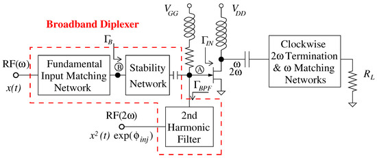
Figure 1.
Circuit blocks for the clockwise loaded class-J PA wih input second-harmonic injection using a broadband diplexer.
This paper is organized as follows. The source-pull simulations and the broadband diplexer design technique will be discussed in detail in Section 2. Section 3 reports the measured results obtained using both CW and chirp radar signals. A conclusion summarizing the contributions is given in Section 4.
2. Broadband Input Network Design Using Input Second-Harmonic Injection
The second-harmonic source-pull simulation results will be first presented. The source-pull simulation setup includes:
- A CREE 15 Watts GaN HEMT transistor (CGH27015) model is used.
- As reported in [3], the transistor gate bias is set at −3 V with a frequency-agile drain supply voltage ranging from 23 to 31.6 V.
- The broadband output matching network of the clockwise-loaded class-J PA reported in [3] is used.
- No physical IMN is used for the simulated source-pull efficiency contours.
- To account for the mismatch in the absence of the IMN, the input one-tone source fundamental power levels were calculated based on constant 40.3 dBm maximum output power and power gain. At 1.9, 2, and 2.1 GHz, the fundamental input power are 25.0, 26.4, and 26.7 dBm, respectively.
- The amplitude and phase of the second-harmonic source reflection coefficient are both swept.
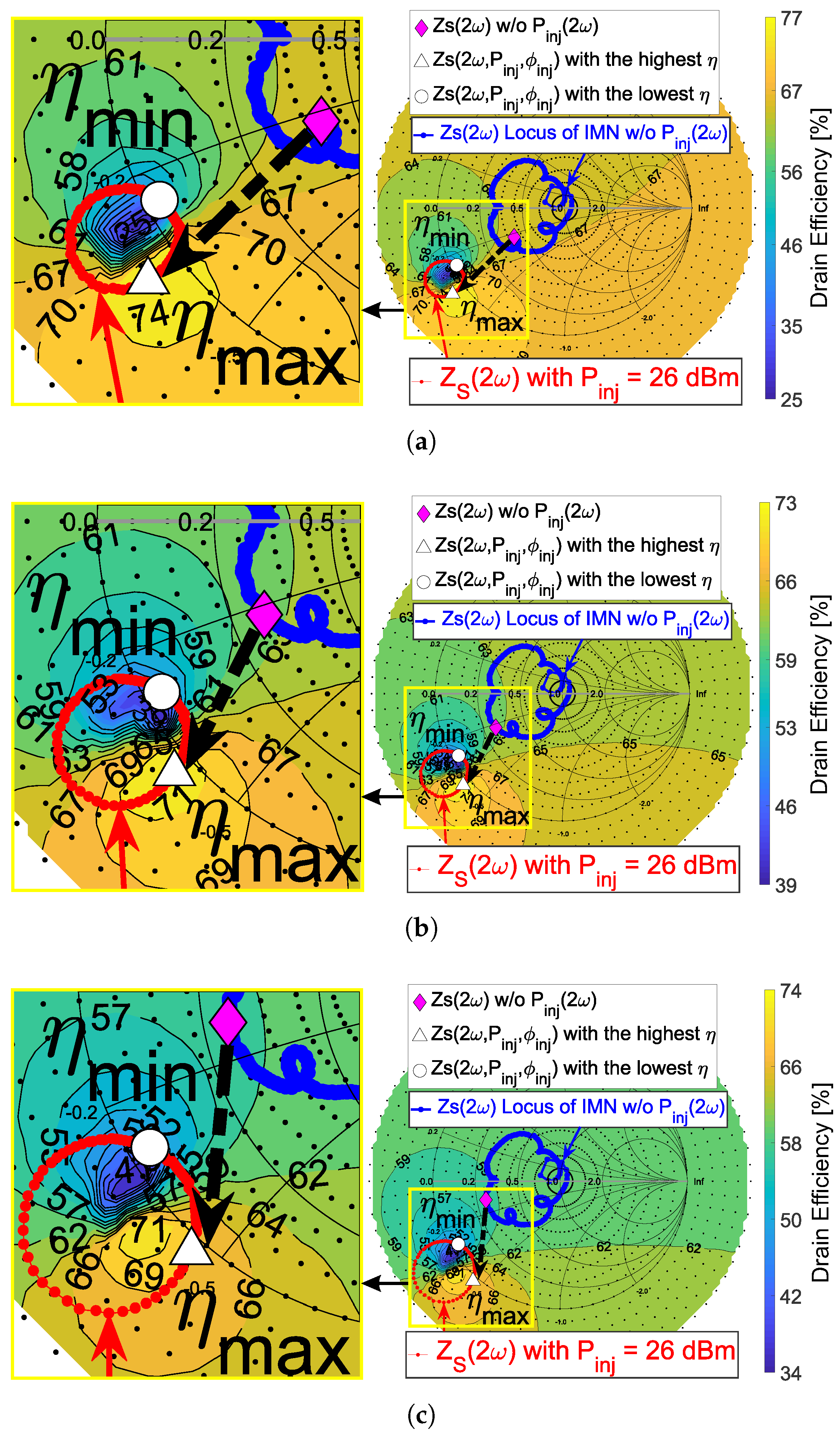
Figure 2 shows the simulated drain-efficiency source-pull contours for at 1.9, 2.0, and 2.1 GHz using the output matching network designed in [3]. The areas with different colors represent different drain efficiencies.
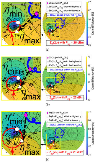
Figure 2.
Simulated drain efficiency source-pull results of the second-harmonic source impedance with constant output power of 40.3 dBm when (a) 1.9 GHz, (b) 2 GHz, and (c) 2.1 GHz. The blue line is the locus at the transistor’s gate package reference plane (PRP) without input second-harmonic injection. The rhombic markers in magenta indicate the of the final IMN at each frequency without input second-harmonic injection. The red dots give the location of the for the specified injected second-harmonic power when the phase of the input second-harmonic signal injection is varied from 0 to . The black dashed arrows indicate the optimal tuning realized by the second-harmonic injection.
The amplitude of was varied from 0 to 1.5 with step size of 0.1. The phase of was varied from 0 to 360 degrees with a step size of 5 degrees. It can be observed that the frequency-dependent maximum-efficiency (in light yellow) and minimum-efficiency (in blue) areas are adjacent to each others along the edge of the Smith chart. Although most of the inside of the Smith chart can yield efficiency above 50%, the maximum-efficiency region above 70% in Figure 2a–c is more desirable. However, it seems impractical to pursue maximum-efficiency regions due to the following reasons:
- The input matching network cannot simultaneously satisfy optimal fundamental conjugate matching and precise second-harmonic control for the broadband design. The second harmonic is often sacrificed and thus uncontrollable.
- The maximum-efficiency and minimum-efficiency regions are too close to each other. It is too risky to pursue optimal because could accidentally fall into the efficiency-minimum region by slight design or fabrication errors.
- The trajectory of the optimal reflection coefficient for the second harmonic is found to rotate anti-clockwise with increasing frequency while following the edge of the Smith Chart, as shown in Figure 3. This indicates that no passive network can be used to realize this non-Foster trajectory.
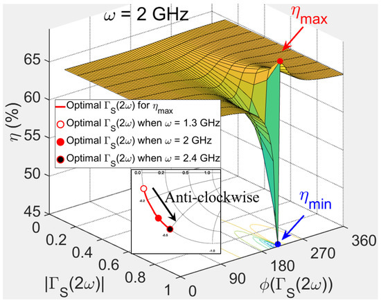 Figure 3. The subfigure shows an anti-clockwise trajectory of optimal input second-harmonic reflection coefficients, which can obtain optimal drain efficiency () from 1.3 to 2.4 GHz. A three-dimensional drain efficiency figure demonstrates its strong dependency to input second-harmonic reflection coefficients.
The above reasons justify the need for the input second-harmonic signal injection.
Based on the source-pull results in Figure 2, the input circuit is designed to place the locus at the PRP (blue line in Figure 2) much closer to the efficiency-extremum regions while remaining in a relatively safe region as indicated. The blue line represents the locus of the designed IMN without injecting an input second-harmonic signal and with varying from 1.3 to 2.4 GHz. The rhombic markers in magenta give for at 1.9, 2.0, and 2.1 GHz.
Given that the reflection coefficients at 1.9, 2.0, and 2.1 GHz are relatively close to the frequency-dependent efficiency-extremum areas, it is still possible that could partially enter the minimum-efficiency regions due to circuit fabrication tolerances, the transistor model accuracy, and fluctuations in device characteristics, which all typically contribute to the discrepancy between the simulation and measurement. Relocating to approach the maximum-efficiency region can be realized by injecting a second-harmonic signal at the gate via a broadband bandpass filter, as shown in Figure 4.
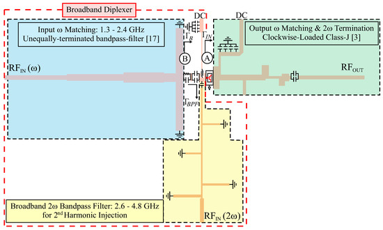
Figure 4.
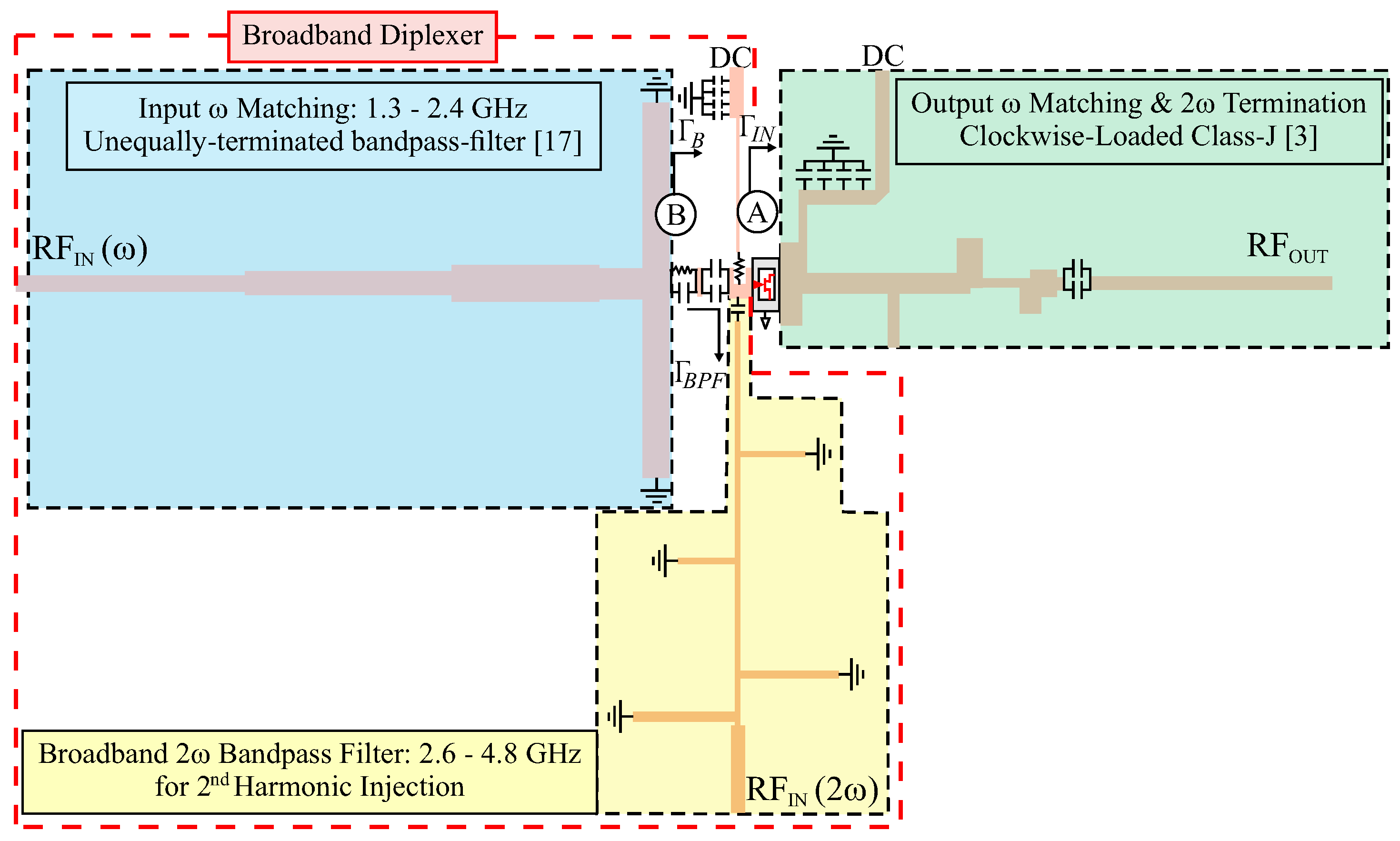
Input and output circuit schematic of the broadband clockwise-loaded class-J (CLCJ) PA.
The input circuit can be divided into three sub-circuits, as shown in Figure 4:
- A bias-tee and stability network;
- A broadband bandpass filter connecting to port for injecting the second-harmonic signal;
- A broadband IMN connecting to port for injecting the fundamental signal.
The input reflection coefficient at the transistor’s gate PRP and de-embeded input reflection coefficient are demonstrated at node A and B in Figure 1, respectively.
For the input circuit design, the stability RC network and bias tee in Figure 4 are optimized such that the impedance (associated with ) provides a constant real part that can be well-fitted with a series RLC circuit. This RLC circuit facilitates the design of the fundamental broadband matching using the unequally terminated bandpass-filter prototype method [17]. Next, the broadband bandpass filter shown in Figure 4 is realized with four short-circuited shunt stubs.
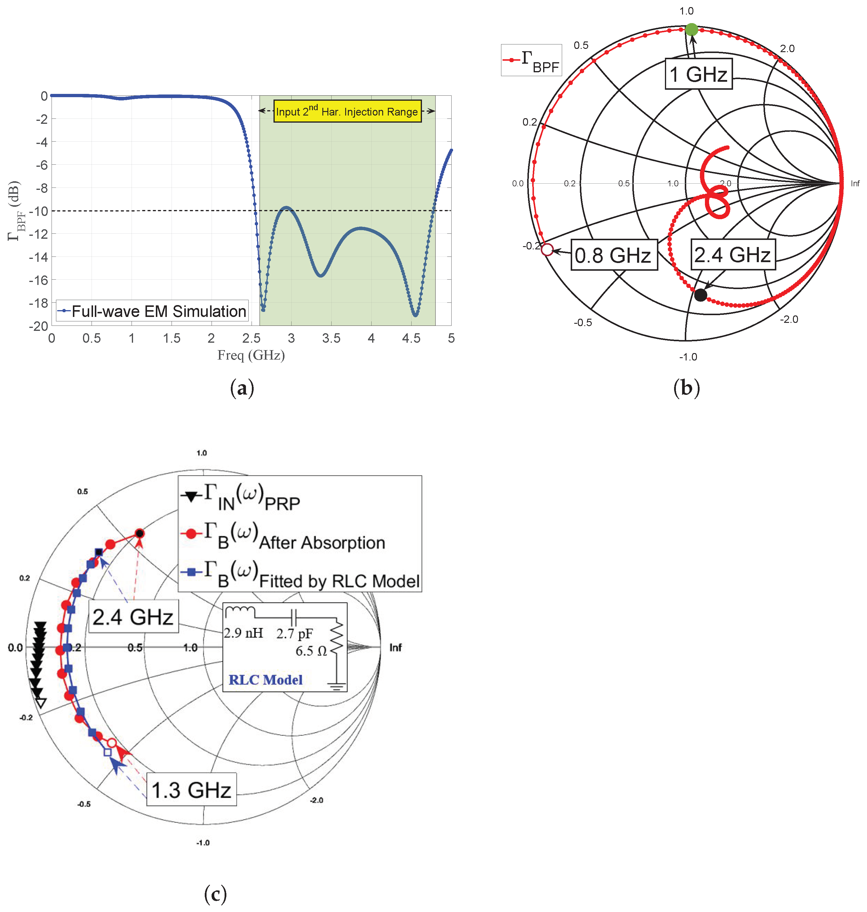
Figure 5a,b show the reflection coefficient of the designed filter. The synthesized is moving along the Smith chart edge from 1.3 to 2.4 GHz in the stop band to block the fundamental signal appearing at node A in Figure 1. From 2.6 to 4.8 GHz, the is designed to be lower than −10 dB for passing through the second-harmonic signal. accounts for the transistor input cascaded with the aforementioned stability, bias-tee, and second-harmonic BPF networks. It can be observed in Figure 5c that (red line with circles) is reasonably well-fitted by an RLC circuit (blue line with squares) from 1.3 to 2.4 GHz. Finally, for simplicity, a low-order broadband IMN is selected to minimize any possible discrepancy between the simulation and measurement due to fabrication errors.
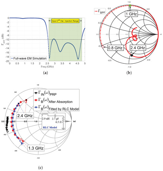
Figure 5.
The design of the IMN diplexer with a broadband bandpass/bandstop filter for the input fundamental and second-harmonic signals, respectively, with: (a) the amplitude of designed from 0 to 5 GHz, (b) designed from 0.8 to 4.8 GHz, and (c) , and the RLC model fitted as part of the input wideband matching network.
Using the designed input circuit as stated above, the amplitude and phase of the injected second-harmonic CW signal are swept at port to approach the maximum-efficiency area. The red dot circles in Figure 2a–c give, for each frequency from 1.9 to 2.1 GHz, the location of the source impedance for the specified injected second-harmonic power dBm when the phase of the injected input second-harmonic signal is varied from 0 to in the simulation. It is observed that the input power of the injected signal can be selected such that the red dots pass through the maximum-efficiency region. The white triangles and circles indicate the active source impedances that yield the highest and lowest drain efficiencies, respectively.
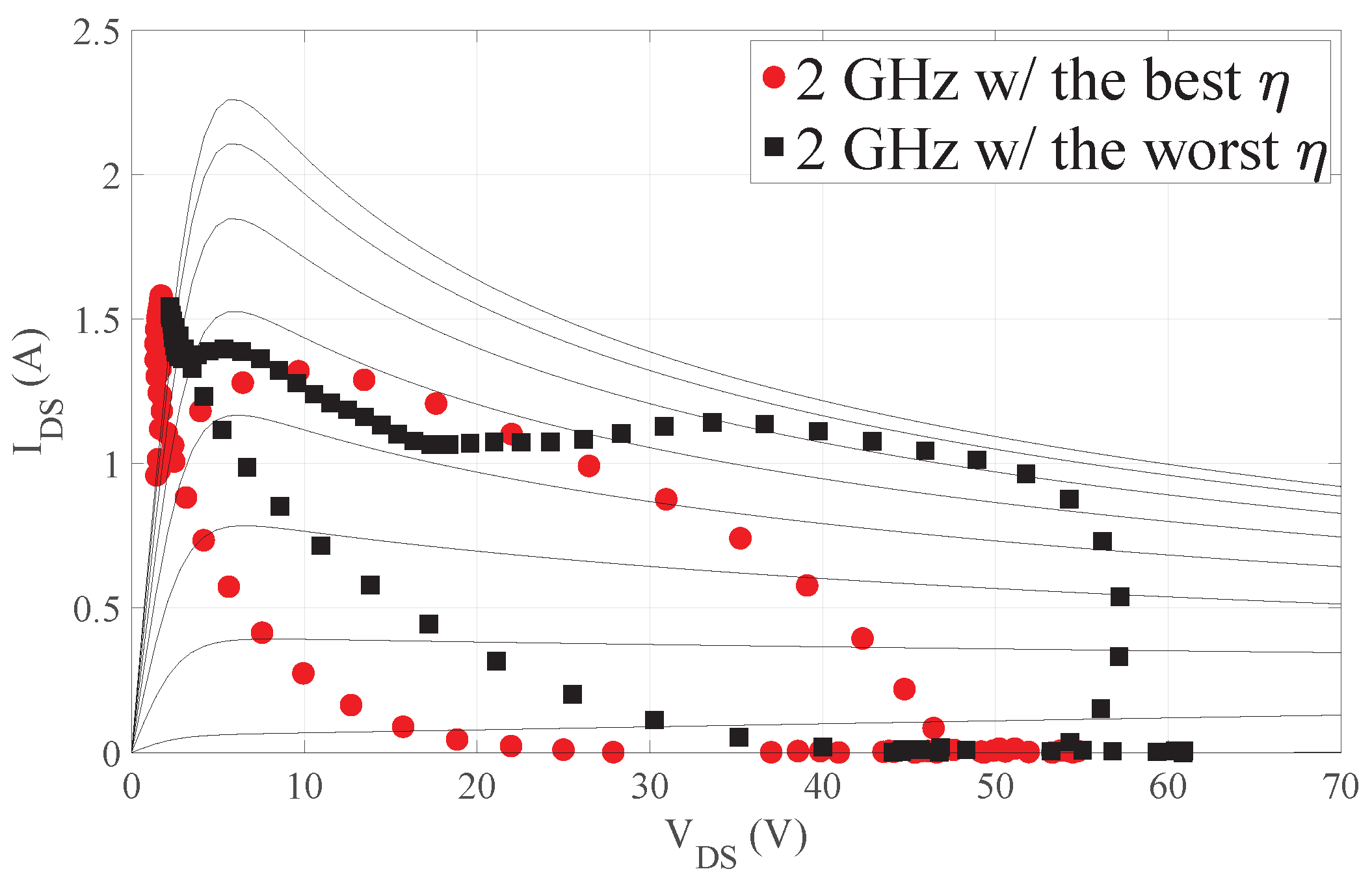
Figure 6 shows the intrinsic loadlines at 2 GHz associated with the best (red) and worst (black) drain efficiencies with the corresponding active source impedances represented by the white triangles and circles in Figure 2. As is verified in Figure 6, the second-harmonic signal injected at the transistor’s gate is effectively tuning the intrinsic drain loadline at the CSRF. These simulations validate the low-power second-harmonic injection technique at the gate, which will be used experimentally in Section 3 to further optimize the drain efficiency. Note that in previously reported works [18,19,20,21], the second-harmonic signal was injected at the drain of the packaged transistor. The advantage of the broadband injection scheme proposed here is that less power is required since the second-harmonic signal is injected at the gate of the packaged transistor using an embedded broadband diplexer.
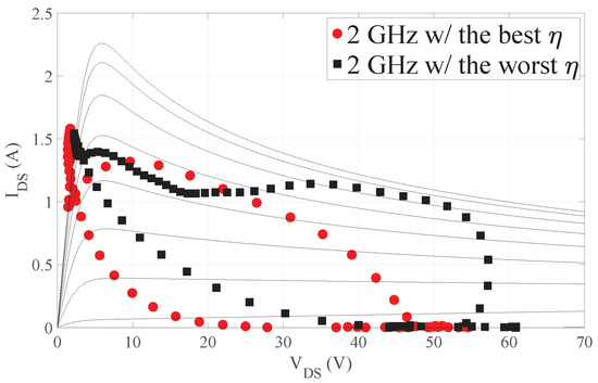
Figure 6.
Comparison of the 2 GHz simulated intrinsic loadlines of the clockwise-loaded class-J PA with 21 dBm second-harmonic injection for the phases yielding the best (red) and worst (black) efficiencies.
3. Experimental Validation Using CW and Modulated Signals
The experimental results are presented in this section. The frequency-agile broadband clockwise-loaded class-J PA circuit and measurement setup were reported in [3]. The fabricated CLCJ PA is shown in Figure 4.
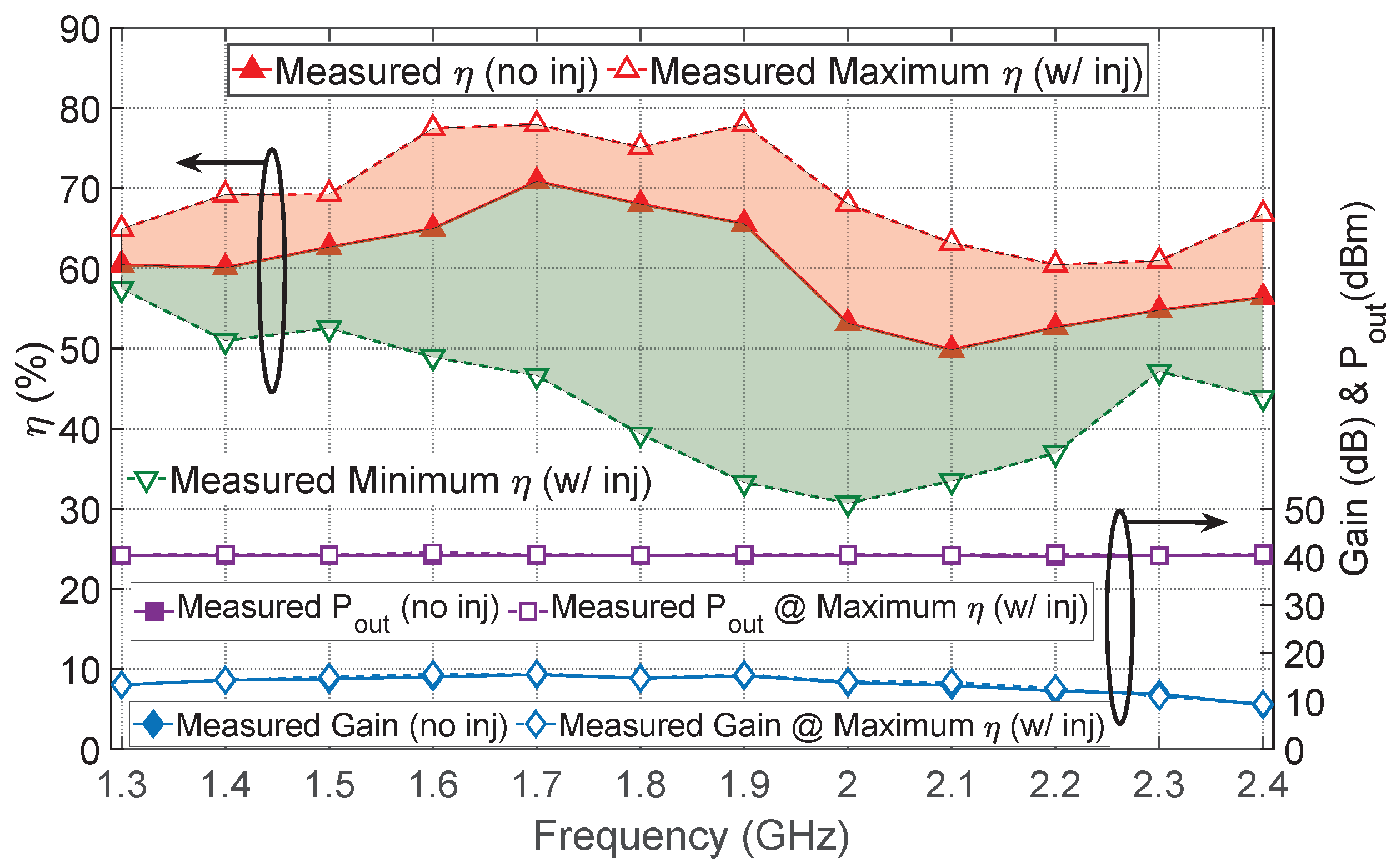
This frequency-agile PA measured with a fundamental CW signal from 1.3 to 2.4 GHz exhibits a constant power (40.3 dBm) throughout the entire fundamental bandwidth, as shown in Figure 7. It should be noted that the fundamental input power is adjusted to obtain constant output power (40.3 dBm) without input second-harmonic injection. Its measured drain efficiency is also well-controlled without using input second-harmonic injection as the drain efficiency remains between 60% and 70% from 1.3 to 1.9 GHz, as shown in Figure 7 (red filled triangles). However, a sharp decrease in efficiency can be observed between 2 and 2.1 GHz due to the discrepancy between the simulated and fabricated circuits, as discussed in Section 2.

Figure 7.
Simulation and CW measurement results before and after second-harmonic injection using the clockwise-loaded class-J theory with low gain compression.
An input second-harmonic signal can then be injected at port RF() to actively approach the maximum efficiency region. To determine the optimal phase and amplitude on the second-harmonic required at the input RF(), the input second-harmonic power is swept from 21 to 26 dBm and the phase from −180 to 180 by steps of 20. Both the maximum and minimum efficiencies under the second-harmonic injection are plotted in Figure 7.
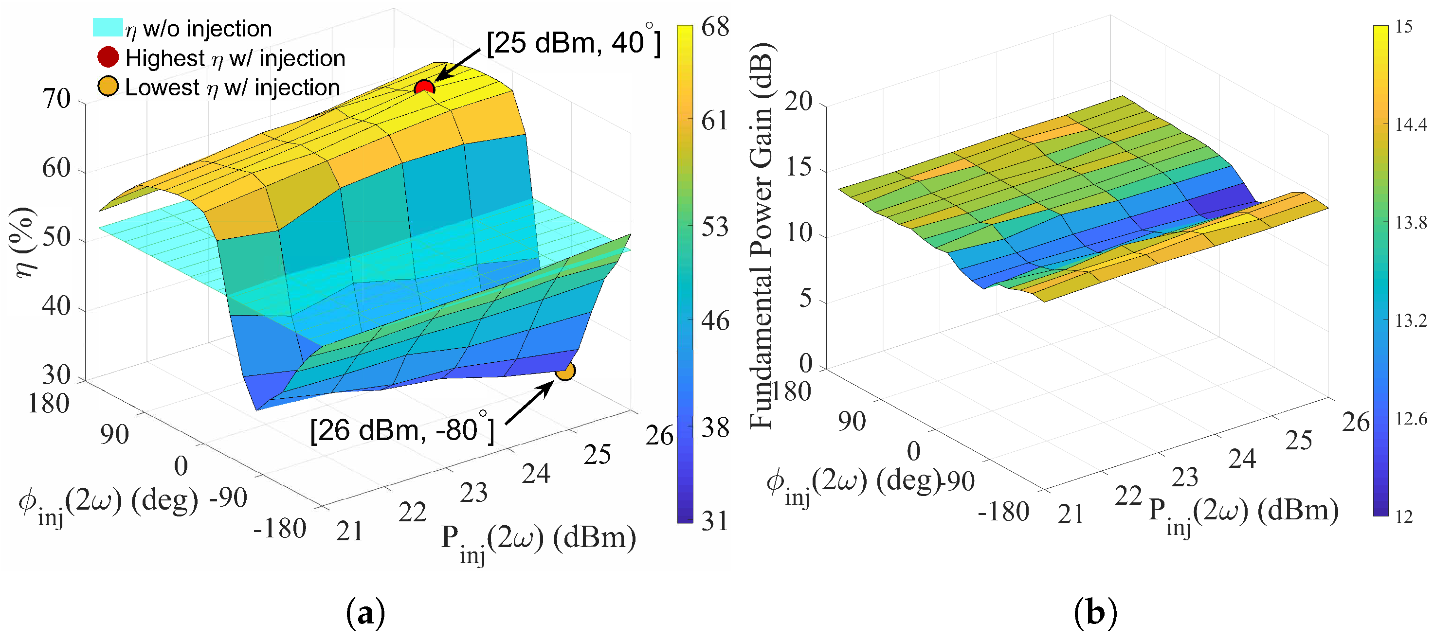
As an example, the dependence of the drain efficiency and fundamental power gain at 2 GHz upon the phase and incident power of the second-harmonic signal injected at port is presented in the three-dimentional plot shown in Figure 8.
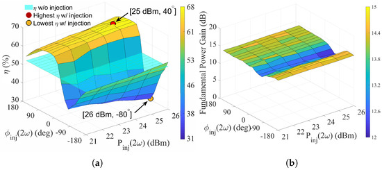
Figure 8.
Measured (a) drain efficiency and (b) fundamental power gain with input CW second-harmonic injection at 4 GHz.
The measured drain efficiency is observed at 2.0 GHz to vary from 31% to 68% as the phase varies within the range of injected second-harmonic power considered. The minimum and maximum efficiencies occur when (P, ) are (26 dBm, −80) and (25 dBm, 40), respectively. It should be noted that the maximum efficiency along (yellow region in Figure 8a) is weakly dependent on the amplitude of the injected input second-harmonic signal. It is more sensitive to the phase of injected input second-harmonic signal. The variation range of the measured drain efficiency is comparable to the variation range of the simulated drain efficiency (39% to 73%) obtained in Figure 2b.
The power and phase sweeps for the input second-harmonic applied at port RF are performed from 1.3 to 2.4 GHz in steps of 0.1 GHz to determine the required optimal second-harmonic injection yielding the highest efficiency. The resulting optimal efficiency under input second-harmonic injection is plotted in Figure 7 using white-filled red triangles. The red-shaded area in Figure 7 highlights the improvements in drain efficiency resulting from the input second-harmonic injection. The measured drain efficiencies are improved from 53% to 68% and 50% to 63% at 2 and 2.1 GHz, respectively. An average of 9.36% in drain efficiency improvement can be achieved from 1.3 to 2.4 GHz.
Finally, measurements using a frequency-modulated chirp radar signal are reported to further validate the practicality of the proposed technique. A 30 MHz fundamental chirp radar signal is injected at port RF simultaneously with a 60 MHz time-synchronized second-harmonic chirp signal injected at port RF with a constant phase offset , as indicated in Figure 1. The power of the injected fundamental and second-harmonic signals are 26.5 dBm and 21 dBm, respectively, while the phase offset is swept from −150 to 180 degrees in steps of 30 degrees.
The power-added efficiency (PAE) is redefined, as shown in Equation (1), to include the injected input second-harmonic power:
where is the efficiency (50%) of a class-A driver PA.
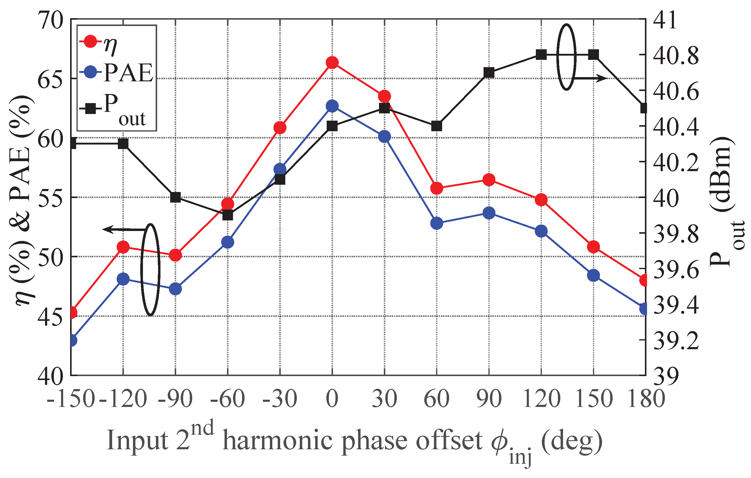
Figure 9 shows that the drain efficiency and PAE defined in Equation (1) are very sensitive to the input second-harmonic phase offset even when its power level is relatively low (21 dBm) compared to the incident power of the fundamental signal (26.5 dBm). Under the above measuring conditions, the drain efficiency varies from 45% to 66.3% with only 0.7 dB of output power variation. Thus, the low-power second-harmonic injection at the gate offers a viable option to assist the IMN in better tracking the maximum-efficiency region.
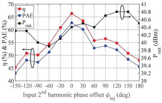
Figure 9.
Measured drain efficiency, PAE, and output power using 30 MHz fundamental chirp signal while injecting a 60 MHz time-synchronized second-harmonic chirp signal at 2 GHz.
Table 1 summarizes the measurement results with CW and modulated chirp radar signals before and after the input second-harmonic injection. The results reported in Table 1 are also compared to previous reports in the literature. In contrast to these reports, broadband operation is demonstrated for the first time with our approach where the diplexer is embedded in the input matching circuit. Note that this is also the first time that the second-harmonic injection is reported using modulated signals (60 MHz bandwidth). An improvement in drain efficiency of 9.7 % is demonstrated for the 30 MHz chirp radar signal used in this work.

Table 1.
Measurements with and without input second-harmonic injection.
4. Conclusions
Broadband efficiency enhancements using input second-harmonic injection is experimentally verified in this article for the first time for both CW and modulated signals when using an embedded broadband diplexer design. The second-harmonic signal is injected through the embedded broadband bandpass filter at the gate of the packaged transistor to further enhance the efficiency via the tuning of the intrinsic output loadlines of the transistor. The effectiveness of the CW and modulated active second-harmonic injection methodology presented in this paper are validated by the improvements in the efficiency experimentally reported in [3]. At 2 GHz, it can be observed that the drain efficiency improves by 15% for CW signals and 9.7% for a frequency-modulated 30 MHz chirp signal. Significant efficiency improvements of 9.4% (from 59.9% to 69.3% in average) can be observed in the frequency range from 1.3 to 2.4 GHz when using harmonic injection. For broadband power amplifier design, the input second-harmonic injection technique is demonstrated in this paper to be a good candidate to (1) realize the non-Foster (anti-clockwise) and active (outside the Smitch Chart) trajectory required for the optimal second-harmonic reflection coefficient and (2) compensate for the inevitable discrepancies between the simulation and measurement, especially for a high-order broadband input matching network.
Author Contributions
Conceptualization, H.-C.C., P.R. and C.L.; methodology, H.-C.C. and P.R.; software, H.-C.C., Y.H., J.I.M.-L. and C.L.; validation, H.-C.C., Y.H. and J.I.M.-L.; formal analysis, H.-C.C.; investigation, H.-C.C.; resources, P.R.; data curation, H.-C.C., Y.H. and J.I.M.-L.; writing—original draft preparation, H.-C.C.; writing—review and editing, P.R. and J.I.M.-L.; visualization, H.-C.C., Y.H., J.I.M.-L. and C.L.; supervision, P.R.; project administration, P.R.; funding acquisition, P.R. All authors have read and agreed to the published version of the manuscript.
Funding
This research was funded by National Science Foundation grant number 1711278.
Data Availability Statement
Part of the data presented in this study are available in [3].
Acknowledgments
Jose I. Martinez-Lopez gratefully acknowledges financial support from the Programa de Apoyos para la Superación del Personal Académico de la UNAM (DGAPA-PASPA).
Conflicts of Interest
The authors declare no conflict of interest.
References
- Cripps, S.C.; Tasker, P.J.; Clarke, A.L.; Lees, J.; Benedikt, J. On the continuity of high efficiency modes in linear RF power amplifiers. IEEE Microw. Wirel. Compon. Lett. 2009, 19, 665–667. [Google Scholar] [CrossRef]
- Wright, P.; Lees, J.; Benedikt, J.; Tasker, P.J.; Cripps, S.C. A Methodology for Realizing High Efficiency Class-J in a Linear and Broadband PA. IEEE Trans. Microw. Theory Tech. 2009, 57, 3196–3204. [Google Scholar] [CrossRef]
- Chang, H.C.; Roblin, P.; Hahn, Y.; Martinez-Lopez, J.I.; Liang, C.; Rawat, K. Frequency-Agile Class-J Power Amplifier With Clockwise Fundamental- and Second-Harmonic Loads. IEEE Trans. Microw. Theory Tech. 2020, 68, 3184–3196. [Google Scholar] [CrossRef]
- Carrubba, V.; Clarke, A.L.; Akmal, M.; Lees, J.; Benedikt, J.; Tasker, P.J.; Cripps, S.C. On the Extension of the Continuous Class-F Mode Power Amplifier. IEEE Trans. Microw. Theory Tech. 2011, 59, 1294–1303. [Google Scholar] [CrossRef]
- Aggrawal, E.; Rawat, K.; Roblin, P. Investigating continuous class-F power amplifier using nonlinear embedding mode. IEEE Microw. Wirel. Compon. Lett. 2017, 27, 593–595. [Google Scholar] [CrossRef]
- Moon, J.; Jee, S.; Kim, J.; Kim, J.; Kim, B. Behaviors of class-F and class-F−1 amplifiers. IEEE Microw. Wirel. Compon. Lett. 2012, 60, 1937–1951. [Google Scholar] [CrossRef]
- Chen, K.; Peroulis, D. Design of Broadband Highly Efficient Harmonic-Tuned Power Amplifier Using In-Band Continuous Class-F−1/F Mode Transferring. IEEE Trans. Microw. Theory Tech. 2012, 60, 4107–4116. [Google Scholar] [CrossRef]
- Alizadeh, A.; Medi, A. Investigation of a Class-J Mode Power Amplifier in Presence of a Second-Harmonic Voltage at the Gate Node of the Transistor. IEEE Trans. Microw. Theory Tech. 2017, 65, 3024–3033. [Google Scholar] [CrossRef]
- Sharma, T.; Srinidhi, E.R.; Darraji, R.; Holmes, D.G.; Staudinger, J.; Jones, J.K.; Ghannouchi, F.M. High-Efficiency Input and Output Harmonically Engineered Power Amplifiers. IEEE Trans. Microw. Theory Tech. 2018, 66, 1002–1014. [Google Scholar] [CrossRef]
- Sharma, T.; Holmes, D.G.; Darraji, R.; Srinidhi, E.R.; Staudinger, J.; Jones, J.K.; Ghannouchi, F.M. On the Second-Harmonic Null in Design Space of Power Amplifiers. IEEE Microw. Wirel. Compon. Lett. 2018, 28, 600–602. [Google Scholar] [CrossRef]
- Sharma, T.; Shukla, S.; Holmes, D.G.; Darraji, R.; Jones, J.K.; Ghannouchi, F.M. Input Harmonic Sensitivity in High-Efficiency GaN Power Amplifiers. In Proceedings of the 2018 IEEE/MTT-S International Microwave Symposium-IMS, Philadelphia, PA, USA, 10–15 June 2018; pp. 461–464. [Google Scholar]
- Dhar, S.K.; Sharma, T.; Darraji, R.; Holmes, D.G.; Illath, S.V.; Mallette, V.; Ghannouchi, F.M. Investigation of Input–Output Waveform Engineered Continuous Inverse Class F Power Amplifiers. IEEE Trans. Microw. Theory Tech. 2019, 67, 3547–3561. [Google Scholar] [CrossRef]
- Dhar, S.K.; Sharma, T.; Zhu, N.; Darraji, R.; Mclaren, R.; Holmes, D.G.; Mallette, V.; Ghannouchi, F.M. Input-Harmonic-Controlled Broadband Continuous Class-F Power Amplifiers for Sub-6-GHz 5G Applications. IEEE Trans. Microw. Theory Tech. 2020, 68, 3120–3133. [Google Scholar] [CrossRef]
- Ramadan, A.; Martin, A.; Nebus, J.-M.; Bouysse, P.; Lapierre, L.; Villemazet, J.F.; Forestier, S. Efficiency enhancement of GaN power HEMTs by controlling gate-source voltage waveform shape. In Proceedings of the 2009 European Microwave Integrated Circuits Conference (EuMIC), Rome, Italy, 28–29 September 2009. [Google Scholar]
- Ramadan, A.; Martin, A.; Nebus, J.M.; Bouysse, P.; Lapierre, L.; Villemazet, J.F.; Forestier, S. Experimental study on effect of second-harmonic injection at input of classes F and F−1 GaN power amplifiers. IET Electron. Lett. 2010, 46, 570–572. [Google Scholar] [CrossRef] [Green Version]
- Haynes, M.; Cripps, S.C.; Benedikt, J.; Tasker, P.J. PAE improvement using 2nd harmonic source injection at X-band. In Proceedings of the 2012 Workshop on Integrated Nonlinear Microwave and Millimetre-wave Circuits, Dublin, Ireland, 3–4 September 2012; pp. 1–3. [Google Scholar]
- Gowrish, B.; Rawat, K.; Basu, A.; Koul, S.K. Broadband matching network using band-pass filter with device parasitic absorption. In Proceedings of the 82nd ARFTG Microwave Measurement Conference, Columbus, OH, USA, 18–21 November 2013; pp. 1–4. [Google Scholar]
- Dani, A.; Roberg, M.; Popovic, Z. PA Efficiency and Linearity Enhancement Using External Harmonic Injection. IEEE Trans. Microw. Theory Tech. 2012, 60, 4097–4106. [Google Scholar] [CrossRef]
- AlMuhaisen, A.; Lees, J.; Cripps, S.C.; Tasker, P.J.; Benedikt, J. Wide Band High-Efficiency Power Amplifier Design. In Proceedings of the IEEE 6th European Microw. Integrated Circuits Conference, Manchester, UK, 10–12 October 2011; pp. 1–4. [Google Scholar]
- Latha, Y.M.A.; Rawat, K.; Helaoui, M.; Ghannouchi, F.M. Broadband continuous mode power amplifier with on-board harmonic injection. IET Microw. Antennas Propag. 2019, 13, 1402–1407. [Google Scholar] [CrossRef]
- Pazhouhesh, P.; Kitchen, J. A Broadband Class AB Power Amplifier with Second Harmonic Injection. In Proceedings of the IEEE 14th Dallas Circuits and Systems Conference (DCAS), Dallas, TX, USA, 15–16 November 2020; pp. 1–5. [Google Scholar]
Publisher’s Note: MDPI stays neutral with regard to jurisdictional claims in published maps and institutional affiliations. |
© 2021 by the authors. Licensee MDPI, Basel, Switzerland. This article is an open access article distributed under the terms and conditions of the Creative Commons Attribution (CC BY) license (https://creativecommons.org/licenses/by/4.0/).

