Article

Understanding the Performance Characteristics of Computational Storage Drives: A Case Study with SmartSSD

1
Department of Computer Science and Engineering, Seoul National University, Seoul 08826, Korea
2
Department of Game Design and Development, Sangmyung University, Seoul 08826, Korea
*
Author to whom correspondence should be addressed.
Electronics 2021, 10(21), 2617; https://doi.org/10.3390/electronics10212617
Submission received: 11 October 2021 / Revised: 23 October 2021 / Accepted: 25 October 2021 / Published: 26 October 2021
(This article belongs to the Section Semiconductor Devices)

Abstract

:
The emerging computational storage drives (CSDs) provide new opportunities by moving data computation closer to the storage. Performing computation within storage drives enables data pre/post-processing without expensive data transfers. Moreover, large amounts of data can be processed in parallel thanks to the nature of the field-programmable gate array (FPGA) included in CSDs. In a CSD, there are several implementation techniques that support parallel processing, each of which provides a different degree of parallelism. However, without sufficient understanding of the parallel processing techniques of CSD, it can lead to overhead due to misuse rather than benefiting from task offloading. Thus, to exploit the best performance of CSDs, it is important to properly adjust the degree of parallelism of each implementation technique. In this paper, we focus on the study of the differences in CSD performance according to various combinations of parallel processing techniques. To investigate the performance differences, we implement and offload the data verification algorithm to the CSD and analyze the performance and resource utilization. The experimental results show that implementing the data verification algorithm with a sufficient understanding of CSD’s parallel processing techniques can improve the performance by up to 20 times. Moreover, even with the same degree of parallelism, the performance can differ by 59% depending on the combination of implementation techniques. These results imply that proper orchestration of different implementation techniques leads to better performance and efficient resource utilization.

1. Introduction

Computational storage drives (CSDs) are attracting attention from both industry and academia because they provide data processing functionality inside the device where the data reside. CSDs can process large amounts of data without moving data from the storage device to the host, making host resources, such as CPU and memory, available for other tasks. In recent years, different vendors commercialized computational storage with different functionalities. For example, special-purpose CSDs provided by AHA [1], Intel QuickAssist [2], or Microsoft Corsica [3] are available on the market. Meanwhile, general-purpose CSDs, which provide a customizable and programmable platform, are also now becoming commercially available by Samsung [4] and ScaleFlux [5].
The structure of such a CSD can exist in various architectures, as investigated by SNIA [6]. Among them, Samsung SmartSSD® (SmartSSD® is a registered trademark of Samsung Electronics). adopts the architecture in which the field-programmable gate array (FPGA), the SSD controller, the RAM, and the storage media all exist in the device, as shown in Figure 1a. This structure is particularly suitable for tasks that require processing before or after the data are stored on storage media. Examples of data processing include data (de)compression, encryption, decryption, and verification for detecting errors. SmartSSD®, provided by Samsung, very recently introduced general-purpose CSD, which supports a high degree of parallelism because the device contains an FPGA accelerator. Hence, data can be processed before or after being stored in the device without involving the host CPU or memory.
There are several recent studies to accelerate data processing by taking advantage of CSD’s near-storage processing capabilities. Chapman et al. [7] explored big data processing acceleration by offloading SQL query processing functionalities of Spark SQL. They used Samsung SmartSSD® to investigate the performance of executing the data filtering process within the storage device. Lee et al. [8] introduced Samsung SmartSSD® platform details and the performance projection model. They presented preliminary performance results of SmartSSD® in data analytic workloads based on the projection model introduced in the article. Cao et al. [9] developed a system that dispatches scan operations of the relational database into the storage device. They modified Alibaba’s proprietary relational database to allow table scan operations to be performed within the CSDs provided by ScaleFlux [5].
Existing studies have focused on reducing the amount of data movement from the storage device by offloading tasks such as data filtering operations [7,9,10]. Since CSDs have recently become commercially available, related studies have mainly been focused on reducing the amount of data movement and overlooked the implementation techniques for maximizing the performance of CSD itself. The performance of data processing on CSD varies depending on the combinations of parallel processing techniques provided by CSD. For example, CSD misuse without sufficient understanding can result in only 5% utilization of performance, as shown in Figure 2. To achieve the best performance from a CSD and efficient use of given resources, it is important to understand and utilize the various parallel processing technique provided by the CSD. In this study, we focused on investigating the differences in performance of the CSD depending on the various combinations of parallel processing techniques.
There are several implementation techniques for performing parallel processing within the CSD [11,12,13,14], and the combination of each technique affects the performance and resource utilization. Since the CSD resources are limited, it is necessary to understand the difference between each technique for efficient use. To this end, we conducted a case study that provides data verification functionality using the cyclic redundancy check (CRC) algorithm on the SmartSSD®. Under various combinations of each technique configuration, we investigated and analyzed the impact of each technique on performance and resource utilization.
CSDs support several implementation techniques that allow a single task to run simultaneously with a high degree of parallelism. One of them is loop unrolling [12,13], which allows independent operations in the loop to be executed in parallel. To properly utilize the loop unrolling functionality, another parallel processing technique, array partitioning [11], should be applied together. Array partitioning divides a contiguous data area allocated as an array into several individual data areas. Another technique for parallelism is creating multiple instances of a computing unit [14]. The workload is offloaded on the CSD in the form of a computing unit, and multiple instances of the computing unit can be created at the compile time by specifying the number of computing units to be executed concurrently. Because there is a difference in the degree of parallelism supported by each technique, the combination of each technique leads to a difference in performance and resource utilization.
As a case study, we implemented and offloaded the data verification algorithm on Samsung SmartSSD® [4], which is the industry’s first customizable, programmable CSD. We performed empirical experiments under various combinations of each implementation technique that support parallel processing with Samsung SmartSSD® (For this study, we received pre-commercialized products from Samsung). Specifically, we performed experiments on seven possible implementation combinations with the same degree of parallelism and compared them to the performance of implementation without applying the parallel processing technique. The normalized data verification time between implementation with and without applying the parallel processing technique is shown in Figure 2. The experimental result shows that the data verification time improved by up to 20 times by implementing the proper combination of parallel processing techniques. In order to fully utilize the performance of CSD, it is essential to understand and properly apply the parallel processing techniques provided by CSD. Between implementations with parallel processing techniques, performance is varied by up to 59% depending on the combination. Moreover, resource utilization in the CSD (e.g., LUT, FF, BRAM, etc.) differs by 20%.
In summary, this paper makes the following contributions.
  • We implement the data verification algorithm on Samsung SmartSSD® with various combinations of parallel processing.
  • We analyze the performance of the Samsung SmartSSD® in terms of resource utilization, power consumption, and execution time with various combinations of parallel processing techniques.
  • The experimental results imply that a well-combined degree of parallelism between different implementation techniques is important in terms of performance and resource utilization.
The rest of this paper is organized as follows:
Section 2 describes the background.
Section 3 discusses related work.
Section 4 presents the design and implementation for the case study in detail.
Section 5 shows the experimental results with various combinations of techniques.
Section 6 summarizes our study.
Section 7 concludes this paper.

2. Background

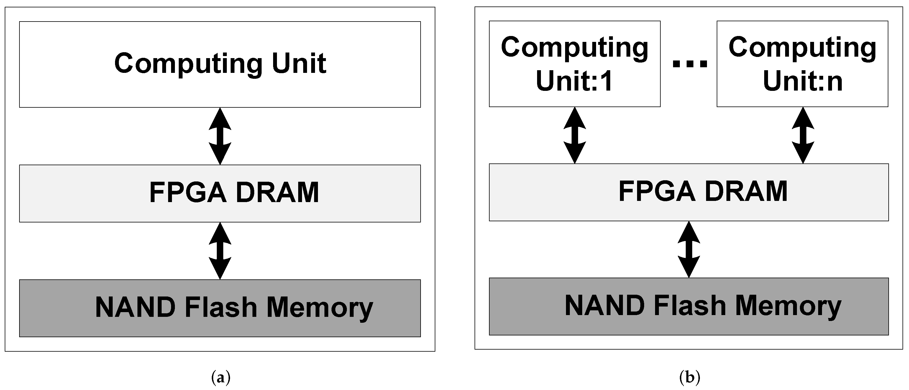
2.1. Architecture of SmartSSD®

Figure 1 shows the hardware architecture of the CSD with respect to the SmartSSD® platform from Samsung [15,16]. The CSD that we used in this study is shown in Figure 1a. For in-storage computation ability, the SmartSSD® platform consists of a Xilinx field programmable gate array (FPGA), which has 8 GB DRAM [17,18] and 1 TB NAND flash memory [19], as a form factor of a PCIe device. The FPGA contains 8 GB DRAM, a buffer space for data transferred between the host memory and the NAND flash memory to enable data processing within the storage device. For example, when compression is performed before storing host memory data to NAND flash memory by exploiting the processing ability of SmartSSD®, the target data are stored in DRAM included in the FPGA to perform compression. When the data transfer between the host memory and the NAND flash memory does not require any intermediate processing (i.e., in-storage processing using FPGA is not involved during data transfer), SmartSSD® operates the same as a commodity SSD (i.e., Samsung PM1733).
Data transfer between the host memory, the FPGA, and the NAND flash memory is performed by a PCIe switch inside the SmartSSD®, as shown in Figure 1b. The SmartSSD® platform provides two different data transfer modes: normal and peer-to-peer (P2P) mode. When data are transferred between the host memory and the NAND flash memory, the PCIe switch operates as a normal mode, whereas the PCIe switch operates as a P2P mode to transfer data between the NAND flash memory and the FPGA DRAM. The application implements in-storage processing functionality with the assistance of the Xilinx OpenCL framework [20] to control P2P communication and manipulate data in the P2P mode.

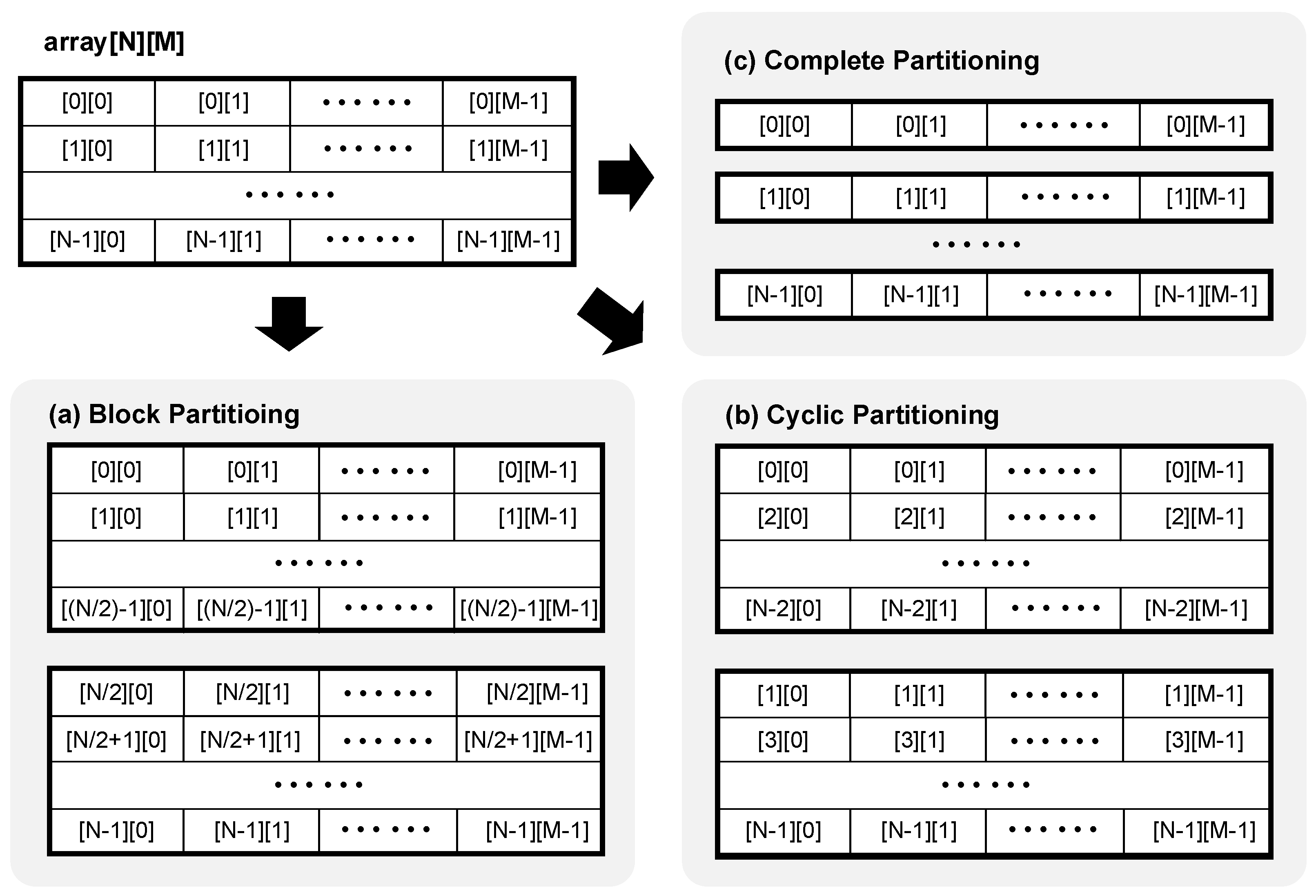
2.2. Techniques for Concurrent Processing within CSD

CSDs provide several implementation techniques to support concurrent processing of data. In the following sections, we introduce techniques utilized in this study.
(1) Array Partitioning: The array is an efficient data structure in terms of program complexity, but within the CSD, it causes long data access times because large data are stored in the external memory, DRAM. To reduce data access time, a large array can be divided into several smaller arrays or individual elements, allowing data to be stored in the on-chip memory, Block RAM (BRAM) (Block RAMs are used for storing read-only data inside the FPGA).
In SmartSSD®, three types of array partitioning are supported; block, cyclic, and complete. Figure 3 illustrates an example in which the array partitioning techniques are applied to a two-dimensional array with a partitioning factor of two. The block array partitioning technique divides the original array into multiple arrays of the same size, as shown in Figure 3a. The number of small arrays to be divided is specified as a factor. Elements of the original array are sequentially assigned to a small array so that consecutive elements are allocated to the same small array. Figure 3b shows how cyclic partitioning divides an array. The cyclic array partitioning technique also divides the original array into multiple arrays of the same size. However, unlike block partitioning, cyclic partitioning assigns elements to each array in cyclic order. Lastly, as can be seen in Figure 3c, complete array partitioning divides the original array into individual elements so that each element is considered as a register.
For example, consider an array size of N with a partitioning factor of 2, as shown in Figure 3. If an application selects the block partitioning technique, the array elements from 0 to ( N 1 ) 2 constitute the first array, and the remaining elements from N 2 to N 1 constitute the second array. On the other hand, if an application selects the cyclic array partitioning technique, the array elements 0, 2, ..., N 4 , N 2 constitute the first array, and the other elements 1, 3, ... N 3 , N 1 constitute the second array. This array partitioning technique can be applied to the multi-dimensional array by specifying that the target dimension is to be split.
In this study, we reshape the data into a two-dimensional array of 4-KB units and apply complete partitioning to dimension 1, so that d a t a s i z e 4 K B individual arrays are generated.
(2) Loop Unrolling: Loop unrolling shortens loop execution time by reducing the number of iterations of the loop. Loop unrolling enables parallel execution of independent operations by generating multiple copies of the loop body. For example, as shown in Figure 4, the number of loop iterations is N in the original code, whereas after loop unrolling is applied, it is reduced to N 4 . However, redundant code generated by loop unrolling causes the overhead of increasing the code size and required registers.
(3) Multiple Computing Units: Another way to exploit parallelism in SmartSSD® is to generate multiple instances of a computing unit at compile-time and place them together in the CSD. Figure 5 depicts the brief architecture of SmartSSD® with different numbers of computing units. Basically, each computing unit is created as a single instance, as shown in Figure 5a, but we can specify the number of kernel instances to be created by the compilation configuration with an option –nk. The maximum number of computing units that can be created is determined dynamically based on the available resource in the computational storage and the resource usage of the computing unit. In other words, even if the number of available resources in computational storage is large, if the code cannot efficiently utilize the resources, we cannot maximize the parallelism of the application.

3. Related Work

3.1. Near-Storage Data Processing

There have been several studies to improve performance by exploiting near-storage data processing.
Zhang et al. [21] and Sun et al. [22] proposed acceleration solutions for LSM-based key-value stores by offloading compaction tasks to the FPGA. They perform the compaction task, which is considered the main cause of performance degradation, in the dedicated FPGA, so that the host resources are concentrated on normal operations. Zhang et al. [21] modified Alibaba’s proprietary LSM-based key-value store, X-Engine, whereas Sun et al. [22] modified LevelDB to verify the effectiveness of their schemes. Ajdari et al. proposed FIDR [23] and CIDR [24]: storage systems that provide data reduction functionality, such as deduplication and compression. Both implement each function, including data signature generation, compression, and decompression, on a dedicated FPGA board, which independently accelerates each function.
Our study is similar to these studies [21,22,23,24] in that it reduces resource utilization of the host systems by offloading tasks to the dedicated device. On the other hand, we focus on investigating the performance difference according to the combinations of parallel processing techniques within the CSD.
Schmid et al. [25] introduced a framework to facilitate the development of applications on systems consisting of heterogeneous hardware. They provide operator structures for developers to define functional units, translating the operator into low-level circuit implementations within the framework. Akagić et al. [26] investigated tradeoffs between implementations utilizing different resources of the FPGA. Specifically, they compare implementation of algorithms for generating CRC, based on utilizing LUTs or BRAM. They analyzed the performance benefits of LUT- and BRAM-based implementations for different slice and processing bit sizes in terms of throughput, achievable clock speed, and hardware cost.
Our study is in line with these works [25,26] in terms of investigating mechanisms for the efficient use of hardware devices that provide near-storage computational capabilities. However, we deploy a data verification algorithm to analyze the performance and resource utilization with the viable CSD, SmartSSD®.

3.2. CSDs

Over the past decade, both industry and academia have paid attention to the possibilities of CSDs.
Hu et al. [27] suggested QZFS that integrate special-purpose CSDs into a ZFS file system. Specifically, they used Intel QuickAssist (QAT) [2], which is a special-purpose CSD for accelerating data compression. Promberger et al. [28] explored the integration cost of numerous compression algorithms with software-based and hardware-based accelerators. They analyzed the cost of each compression algorithm in terms of throughput, power consumption, etc. Gu et al. [10] introduced Biscuit, a framework for near-data processing for data analytic workloads. In their study, the prototypical CSD had a specialized SSD controller that enabled near-data processing and a hardware pattern matcher for each flash memory channel. By filtering out irrelevant data within the storage device, Biscuit reduces the amount of data transferred between the storage device and the host system. Our study is in line with this research [10,27,28] in terms of investigating the effectiveness of CSDs. However, these approaches facilitate special-purpose CSDs, whereas our study focuses on facilitating general-purpose CSDs.
Lee et al. [8] introduced SmartSSD® platform details and performance using the described projection model. Chapman et al. [7] proposed a framework to accelerate query processing of SparkSQL to SmartSSD®. The framework accelerates parts of the query processing procedure by performing them in SmartSSD® based on the cost function that is tuned by offline profiling. Cao et al. [9] presented a framework that offloads table scan operations of the relational database across CSDs that are connected to distributed storage nodes. They deployed the framework in the production database server of Alibaba [29] to demonstrate the feasibility of the CSD in the real world. Our study is similar to these studies [7,8,9] in that we accelerate the task by offloading operations to the viable CSD. In contrast, we focus on studying the performance characteristics of the CSD according to combinations of parallel processing techniques.
Lagrange et al. [30] modeled and analyzed the expected performance when offloading a few tasks in the analytic applications. They estimated the achievable speed-up by offloading a few operations (e.g., scan, filter, and project) to the CSD. Barbalace et al. [31] raised several open challenges to CSDs, including resource management, security, data consistency, and usability. Then, they discussed directions in which well-known programming models can be beneficial to solving such challenges. Our study is in line with these studies [30,31] in terms of the analyzing characteristics of the CSD. However, we analyze the performance characteristics and resource utilization of the CSD using the results of data verification tasks performed on the viable CSD.

4. Case Study: Data Verification

4.1. Design Overview

In this study, we focus on investigating the performance characteristics of CSDs using various combinations of implementation techniques. To do this, we implement an algorithm that can verify data integrity in parallel and deploy it to SmartSSD®. We choose the data verification algorithm as a case study to perform as much parallel processing as possible under limited resources. Figure 6 illustrates the overall architecture of implementation deployed on SmartSSD®. As can be seen in Figure 6, we implement the data verifier as a computing unit. The number of the computing unit is changeable by specifying numbers with option nk at compile time. As shown on the left side of Figure 6, six computing units are created in this architecture. It is possible to change the number of data pages to perform verification on each computing unit, which is a data verifier. The right side of Figure 6 shows a single data verifier that can perform data verification for four data pages concurrently. However, the total number of computing units and data pages that can be executed simultaneously is limited depending on the resource of the CSD, so that we adjust the number of computing units and the number of data pages handled in each data verifier considering such limitations. In the following sections, we provide detailed descriptions of the data verification procedure and implementation details applying various parallel processing techniques.

4.2. Data Verification Procedure

In this section, we describe how we perform data verification for a single file with the architecture as described in the previous section. First, the host system stores a file to SmartSSD® in the same way it stores a file to the commodity storage devices. In order to perform data integrity verification on the files stored in the storage device, the existing systems with the commodity storage device should read the file back into the host system’s memory. During this process, invalidating the page cache of the host system’s memory is required to remove the contents remaining in the host system’s memory [32]. In contrast, when using a CSD, reading the file back into the host system is unnecessary. With the CSD, data integrity verification tasks are performed within the storage device itself, after each file is stored. Therefore, resources of the host system, such as CPU and memory, can be concentrated on tasks other than integrity verification for the stored data.
In particular, with SmartSSD®, the file is first read to the memory within the storage device. The data verification procedure of each data verifier performs integrity verification for data in 4-KB page units, as shown in Figure 6. To do so, the data are transferred to each data verifier in multiples of 4-KB page units through P2P communication. Algorithm 1 briefly describes the data verification procedure. Each data verifier first allocates an array on BRAM and applies the array partitioning as a complete type (line 2). The data are then copied from FPGA DRAM to a local array on BRAM by splitting the data into 4 KB pages so that each page is considered as an individual datum (lines 3–4). The data verifier executes a loop that calculates the checksum value for each page of data. At this point, we apply loop unrolling to the loop that calculates the checksum value so that computations for each page are performed concurrently (lines 5–6).
Algorithm 1 Computing Unit: Data Verification
1:
proceduredata_verify( d a t a )
2:
       a l l o c a t e a r r a y o n B R A M                                                                       ▹ ARRAY_PARTITION
3:
      for each  p a g e s o f d a t a  do
4:
             c o p y d a t a f r o m F P G A D R A M t o l o c a l a r r a y o n B R A M
5:
      for each  p a g e o f d a t a do                                                                                                    ▹ UNROLL
6:
             c o m p u t e c r c v a l u e o f e a c h p a g e

4.3. Implementation

We implement our computing unit, data verifier, using Xilinx High-Level Synthesis (HLS) [33] with Xilinx SDx 2019.1, Linux 4.16.1 kernel. We use HLS pragma directives to apply array partitioning for the data to be verified. We apply array partitioning as a complete type of 4-KB units, so data verification is performed in 4-KB page units, and the page size is configurable. We use HLS pragma directives to apply loop unrolling for the loop that calculates the checksum value to independently execute the checksum computation for each 4-KB page. The creation of multiple computing units is attained by specifying the number of computing units with option nk of the compilation command line.

4.4. Evaluation Scenario

With the data verification algorithm used in this study, the maximum number of individual procedures that perform data verification in units of pages is 300. Therefore, we adjust the number of data verifiers and the number of data pages processed by each data verifier so that the total number of data verification procedures being executed concurrently is 300. To hold the number of the procedures performing integrity verification concurrently to 300, we use seven different combinations of degrees of parallelism: we transfer N data in units of 4 KB, of which the value of N is set to 25, 30, 50, 60, 75, 100, and 150. Accordingly, the number of computing units in each case is 12, 10, 6, 5, 4, 3, and 2, respectively. In addition, we implement a baseline computing unit that performs data verification sequentially to compare the performance with the case where parallel processing techniques are not applied.

5. Performance Analysis

5.1. Experimental Setup

The machine we used in the following experiments is equipped with an Intel Xeon 2-way E5-2620, which has 16 cores with 160 GB memory. We used Samsung SmartSSD® as the CSD, which is a U.2 form factor product in development. There is a slight difference in specifications presented in Figure 1a; the CSD includes 4 GB FPGA DRAM and 3.84 TB NAND flash memory. We implemented and dispatched the data verification algorithm into SmartSSD® so that the verification procedure for the data that are stored on the storage device could be performed within SmartSSD®. As mentioned in Section 4.4, we evaluated the data verification time with various combinations of parallel processing techniques provided by SmartSSD®. Furthermore, we compared the data verification time between implementations with and without parallel processing techniques. Each evaluation point was obtained by averaging the results of 5 independent runs with standard deviations below 6.6% of the mean.

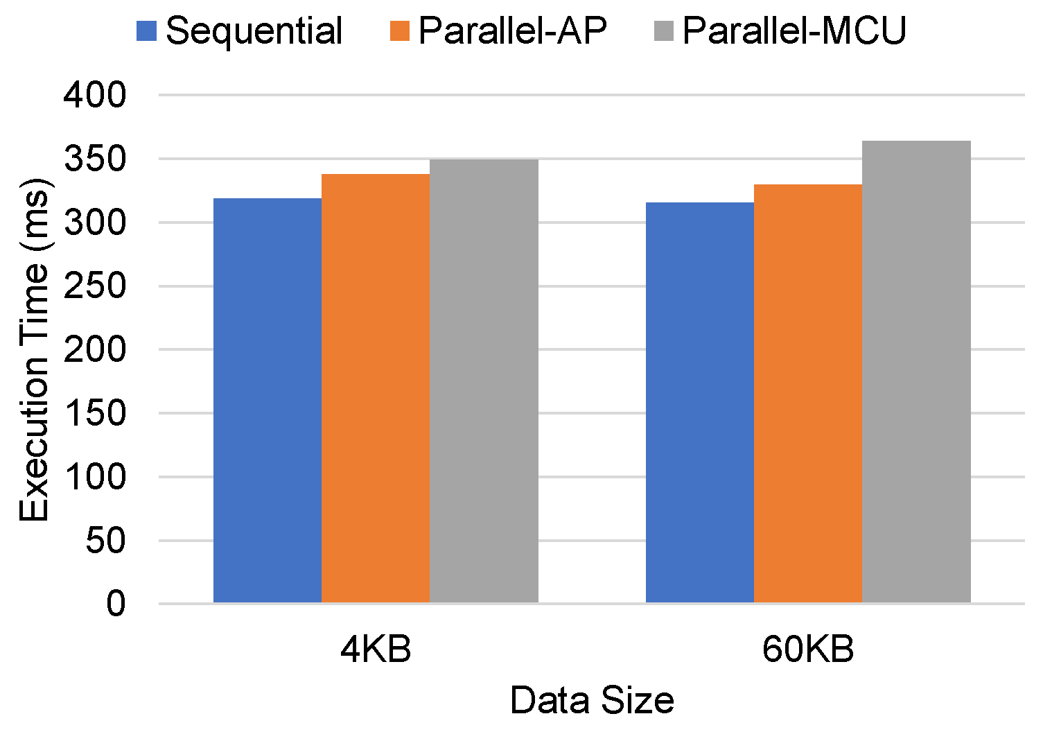
5.2. Single-Page Data Verification Time

To explore the performance difference between different parallel processing techniques, we first evaluated the performance of each implementation technique with a degree of parallelism of one. In other words, we performed data verification with each implementation technique for a single page of data, 4 KB, and 60 KB. Since the maximum number of data verifier computing units that can be placed together on SmartSSD® is 15, we performed data verification for data of size 60 KB, which is 15 times of the 4-KB page. Figure 7 presents the data verification time of 4 KB and 60 KB data with sequential implementation (Sequential), a computing unit with array partitioning (Parallel-AP), and multiple computing units that perform data verification for a single page (Parallel-MCU). As can be seen, when the degree of parallelism is one, the data verification time with sequential implementation shows the best performance.
The reason for the longer execution time of the implementation with parallel processing techniques is due to the initialization overhead. When we use array partitioning, we should copy data from the global memory, the FPGA DRAM, to BRAM. Therefore, with array partitioning, allocating and copying the data on BRAM causes longer execution time compared to the sequential implementation. On the other hand, with multiple computing units, SmartSSD® should load the multiple computing units during the initialization, which causes a longer execution time compared to the other implementations.
In summary, when the data size is small, such as a single page, sequential processing could be a better choice for performance rather than applying array partitioning or processing with multiple computing units. With small data size, applying array partitioning within a single computing unit could yield better performance than processing the data with multiple computing units.

5.3. Multiple-Page Data Verification Time

Figure 8 shows the data verification time of a single file of size 1 GB with various combinations of parallel processing techniques as mentioned in Section 4.4. As shown in Figure 8, the overall data verification time is reduced by up to 59% depending on the combinations of parallel processing techniques. Specifically, when the parallelism of array partitioning is high, and the number of computing units is small, the time for data verification is longer. This means that using multiple computing units is more efficient for the same degree of parallelism than increasing parallelism within a single computing unit. Moreover, the initialization overhead that appeared in the single-page data verification procedure described in Section 5.2 is hidden due to parallel processing as the data size increases.
On the contrary to this trend, when AP × MCU is a 60 × 5 combination, the overall data verification time is shorter than the other time of two adjacent combinations. To understand this singularity, we analyzed the device layout, as shown in Figure 9. The lower part of the device layout for each combination is the static area so that there is no difference between implementations. The part to concentrate on is the upper part of the device layout for each combination. As can be seen in the figures, for higher performance, computing units should be evenly placed over the entire dynamic area of the device.
In addition, we evaluated the data verification time for multiple pages of the implementation without applying parallel processing techniques. Figure 10 presents the execution time of data verification of a single file of size 1 GB without parallel processing techniques (Sequential) and execution time of data verification with parallel processing techniques (Optimized). As can be seen, the data verification time of sequential implementation takes 20-times longer compared to that of the implementation with parallel processing techniques. In other words, when using a CSD, understanding the characteristics of parallel processing and applying it to proper combinations leads to a big difference in performance.

5.4. Resource Utilization

We analyzed the resource utilization of each combination of parallel processing techniques. Table 1 shows the utilization of some representative resources within the CSD. As can be seen from the table, each resource utilization increases as the number of computing units increases. Especially in the case of the 25 × 12 combination, BRAM utilization increases by 30% over the 150 × 2 combination. As a result, more data can be accessed faster with the 25 × 12 combination, resulting in higher performance.

6. Summary and Implications

In this paper, we focused on investigating the performance characteristics of the CSD depending on various combinations of parallel processing techniques. From the evaluations with data verification performed in this paper, we make the following conclusions. First, when the degree of parallelism of the computing unit of the CSD is not higher than a certain level, the initialization overhead can be larger than the performance gain. In particular, when the data size is small, sequential implementation could be a better choice. Second, when the task executed in the CSD can achieve a sufficient level of parallelism, it is important to understand the characteristics of each parallel processing technique provided by the CSD. Each technique has a different parallel processing capability, which results in a different performance depending on the combination. Lastly, since the resources provided by the CSD are limited, the performance can differ even in the same degree of parallelism depending on the layout of the computing units. Therefore, when using multiple computing units, the placement of each computing unit should also be considered for optimal performance.

7. Conclusions

In this paper, we studied the performance characteristics and resource utilization of CSD with various combinations of parallel processing techniques. To understand the characteristics of each technique, we conducted a case study to analyze the differences in the performance of a viable CSD. The experimental results show that depending on the combinations of parallel processing techniques, the performance can differ by up to 59% even with the same degree of parallelism. In addition, depending on the combinations of parallel processing techniques, resource utilization can differ by up to 30%. As can be seen from the evaluation, the difference in performance can be as high as 20 times depending on which parallel processing technique is used; thus, it is important to properly apply the technique that adequately provides concurrency for better performance and efficiently uses the resources of the CSD. As general-purpose CSDs are now starting to be commercialized, we expect that our study can be helpful to understand the performance characteristics of general-purpose CSDs to fully exploit the performance benefits by maximizing their own parallelism. For future work, based on the understanding of the performance characteristics of the CSD, we plan to study the adaptive parallel processing of the data within the CSD.

Author Contributions

Conceptualization, H.K. and H.Y.Y.; methodology, H.K., H.Y.Y. and H.S.; software, H.K.; validation, H.K.; investigation, H.K., H.Y.Y. and H.S.; writing—original draft preparation, H.K.; writing—review and editing, H.K., H.Y.Y. and H.S. All authors have read and agreed to the published version of the manuscript.

Funding

This research was supported by the Next-Generation Information Computing Development Program through the National Research Foundation of Korea (NRF) funded by the Ministry of Science, ICT (2021R1A2C2003618). This work was also supported by the Samsung Electronics Co., Ltd. in Suwon, Korea. (Corresponding author: Hanul Sung).

Data Availability Statement

Not applicable.

Conflicts of Interest

The authors declare no conflict of interest.

References

  1. AHA Prodecuts Group. Available online: http://www.aha.com/ (accessed on 10 October 2021).
  2. Intel QuickAssist Technology Overview. Available online: https://www.intel.com/content/www/us/en/architecture-and-technology/intel-quick-assist-technology-overview.html (accessed on 10 October 2021).
  3. Microsoft Project Corsica. Available online: https://www.servethehome.com/microsoft-project-corsica-asic-delivers-100gbps-zipline-performance/ (accessed on 10 October 2021).
  4. Samsung SmartSSD. Available online: https://samsungsemiconductor-us.com/smartssd/ (accessed on 10 October 2021).
  5. ScaleFlux Computational Storage. Available online: https://www.scaleflux.com/ (accessed on 10 October 2021).
  6. SNIA Computational Storage. Available online: https://www.snia.org/computational (accessed on 10 October 2021).
  7. Chapman, K.; Nik, M.; Robatmili, B.; Mirkhani, S.; Lavasani, M. Computational Storage For Big Data Analytics. In Proceedings of the 10th International Workshop on Accelerating Analytics and Data Management Systems (ADMS’19), Los Angeles, CA, USA, 26 August 2019. [Google Scholar]
  8. Lee, J.H.; Zhang, H.; Lagrange, V.; Krishnamoorthy, P.; Zhao, X.; Ki, Y.S. SmartSSD: FPGA Accelerated Near-Storage Data Analytics on SSD. IEEE Comput. Archit. Lett. 2020, 19, 110–113. [Google Scholar] [CrossRef]
  9. Cao, W.; Liu, Y.; Cheng, Z.; Zheng, N.; Li, W.; Wu, W.; Ouyang, L.; Wang, P.; Wang, Y.; Kuan, R.; et al. POLARDB Meets Computational Storage: Efficiently Support Analytical Workloads in Cloud-Native Relational Database. In Proceedings of the 18th USENIX Conference on File and Storage Technologies (FAST 20), Santa Clara, CA, USA, 25–27 February 2020; pp. 29–41. [Google Scholar]
  10. Gu, B.; Yoon, A.S.; Bae, D.H.; Jo, I.; Lee, J.; Yoon, J.; Kang, J.U.; Kwon, M.; Yoon, C.; Cho, S.; et al. Biscuit: A Framework for Near-Data Processing of Big Data Workloads. In Proceedings of the 2016 ACM/IEEE 43rd Annual International Symposium on Computer Architecture (ISCA), IEEE, Seoul, Korea, 18–22 June 2016; pp. 153–165. [Google Scholar]
  11. SDAccel Environment. Available online: https://www.xilinx.com/html_docs/xilinx2017_4/sdaccel_doc/gle1504034361378.html (accessed on 10 October 2021).
  12. SDAccel Environment. Available online: https://www.xilinx.com/html_docs/xilinx2017_4/sdaccel_doc/rad1504034309598.html (accessed on 10 October 2021).
  13. SDAccel Environment. Available online: https://www.xilinx.com/html_docs/xilinx2017_4/sdaccel_doc/uyd1504034366571.html (accessed on 10 October 2021).
  14. SDAccel Environment. Available online: https://www.xilinx.com/html_docs/xilinx2017_4/sdaccel_doc/yih1504034306435.html (accessed on 10 October 2021).
  15. SmartSSD Computational Storage Drive. Available online: https://samsungatfirst.com/smartssd/ (accessed on 10 October 2021).
  16. Samsung SmartSSD Product Brief. Available online: https://samsungsemiconductor-us.com/labs/pdfs/Samsung_PM983_Product_Brief.pdf (accessed on 10 October 2021).
  17. Xilinx UltraScale+ FPGAs. Available online: https://www.xilinx.com/products/silicon-devices/fpga/kintex-ultrascale-plus.html (accessed on 10 October 2021).
  18. UltraScale+ FPGA Product Tables and Product Selection Guide. Available online: https://www.xilinx.com/support/documentation/selection-guides/ultrascale-plus-fpga-product-selection-guide.pdf (accessed on 10 October 2021).
  19. Samsung PM1733 Product Brief. Available online: https://samsungsemiconductor-us.com/labs/pdfs/PM1733_U2_Product_Brief.pdf (accessed on 10 October 2021).
  20. Fifield, J.; Keryell, R.; Ratigner, H.; Styles, H.; Wu, J. Optimizing opencl applications on xilinx fpga. In Proceedings of the 4th International Workshop on OpenCL, Vienna, Austria, 19–21 April 2016; pp. 1–2. [Google Scholar]
  21. Zhang, T.; Wang, J.; Cheng, X.; Xu, H.; Yu, N.; Huang, G.; Zhang, T.; He, D.; Li, F.; Cao, W.; et al. FPGA-Accelerated Compactions for LSM-based Key-Value Store. In Proceedings of the 18th USENIX Conference on File and Storage Technologies (FAST 20), Santa Clara, CA, USA, 25–27 February 2020; pp. 225–237. [Google Scholar]
  22. Sun, X.; Yu, J.; Zhou, Z.; Xue, C.J. FPGA-based Compaction Engine for Accelerating LSM-tree Key-Value Stores. In Proceedings of the 2020 IEEE 36th International Conference on Data Engineering (ICDE), IEEE, Dallas, TX, USA, 20–24 April 2020; pp. 1261–1272. [Google Scholar]
  23. Ajdari, M.; Lee, W.; Park, P.; Kim, J.; Kim, J. FIDR: A Scalable Storage System for Fine-Grain Inline Data Reduction with Efficient Memory Handling. In Proceedings of the 52nd Annual IEEE/ACM International Symposium on Microarchitecture, Columbus, OH, USA, 12–16 October 2019; pp. 239–252. [Google Scholar]
  24. Ajdari, M.; Park, P.; Kim, J.; Kwon, D.; Kim, J. CIDR: A cost-effective in-line data reduction system for terabit-per-second scale SSD arrays. In Proceedings of the 2019 IEEE International Symposium on High Performance Computer Architecture (HPCA), IEEE, Washington, DC, USA, 16–20 February 2019; pp. 28–41. [Google Scholar]
  25. Schmid, R.; Plauth, M.; Wenzel, L.; Eberhardt, F.; Polze, A. Accessible near-storage computing with FPGAs. In Proceedings of the Fifteenth European Conference on Computer Systems, Heraklon, Greece, 27–30 April 2020; pp. 1–12. [Google Scholar]
  26. Akagić, A.; Amano, H. Performance evaluation of multiple lookup tables algorithms for generating CRC on an FPGA. In Proceedings of the 2011 1st International Symposium on Access Spaces (ISAS), IEEE, Yokohama, Japan, 17–19 June 2011; pp. 164–169. [Google Scholar]
  27. Hu, X.; Wang, F.; Li, W.; Li, J.; Guan, H. QZFS:QAT Accelerated Compression in File System for Application Agnostic and Cost Efficient Data Storage. In Proceedings of the 2019 USENIX Annual Technical Conference (USENIX ATC 19), Renton, WA, USA, 10–12 July 2019; pp. 163–176. [Google Scholar]
  28. Promberger, L.; Schwemmer, R.; Fröning, H. Assessing the Overhead of Offloading Compression Tasks. In Proceedings of the 49th International Conference on Parallel Processing-ICPP: Workshops, Edmonton, AB, Canada, 17–20 August 2020; pp. 1–10. [Google Scholar]
  29. Alibaba.com. Available online: https://www.alibaba.com (accessed on 10 October 2021).
  30. Lagrange Moutinho dos Reis, V.; Li, H.; Shayesteh, A. Modeling Analytics for Computational Storage. In Proceedings of the ACM/SPEC International Conference on Performance Engineering, Edmonton, AB, Canada, 25–30 April 2020; pp. 88–99. [Google Scholar]
  31. Barbalace, A.; Do, J. Computational Storage: Where Are We Today? In Proceedings of the Annual Conference on Innovative Data Systems Research, Chaminade, CA, USA, 10–13 January 2021. [Google Scholar]
  32. Charyyev, B.; Alhussen, A.; Sapkota, H.; Pouyoul, E.; Gunes, M.H.; Arslan, E. Towards securing data transfers against silent data corruption. In Proceedings of the IEEE/ACM International Symposium in Cluster, Cloud, and Grid Computing, IEEE/ACM, Larnaca, Cyprus, 14–17 May 2019. [Google Scholar]
  33. Vitis High-Level Synthesis. Available online: https://www.xilinx.com/products/design-tools/vivado/integration/esl-design.html (accessed on 10 October 2021).
Figure 1. Samsung SmartSSD® (a) hardware architecture (b) (Figure 1 is copyrighted by Samsung Electronics. The image was obtained with permission from https://youtu.be/OHWzWv4gCTs?t=639 (accessed on 10 October 2021)).
Electronics 10 02617 g001
Figure 2. Data verification time.
Electronics 10 02617 g002
Figure 3. Different types of array partitioning techniques; block, cyclic, and complete partitioning.
Electronics 10 02617 g003
Figure 4. Code comparison between original and loop unrolling applied.
Electronics 10 02617 g004
Figure 5. Architecture comparison between sigle and multiple computing units within CSD. (a) Single computing unit with option (–nk CUName:1). (b) Multiple computing unit with option (–nk CUName:n).
Electronics 10 02617 g005
Figure 6. Overall architecture.
Electronics 10 02617 g006
Figure 7. Single-page data verification time.
Electronics 10 02617 g007
Figure 8. Data verification time comparison between combinations of parallel processing techniques.
Electronics 10 02617 g008
Figure 9. Device layout according to various combinations of parallel processing techniques (AP × MCU).
Electronics 10 02617 g009
Figure 10. Data verification time with or without parallel processing.
Electronics 10 02617 g010
Table 1. Resource utilization.
LUTLUTRAMFFBRAM
25 × 12 3382585
30 × 10 3272481
50 × 6 3072273
60 × 5 2972171
75 × 4 3272269
100 × 3 3362167
150 × 2 3162165
Publisher’s Note: MDPI stays neutral with regard to jurisdictional claims in published maps and institutional affiliations.

