Article

A Novel MOS-Channel Diode Embedded in a SiC Superjunction MOSFET for Enhanced Switching Performance and Superior Short Circuit Ruggedness

Department of Electronic Engineering, Sogang University, Seoul 04107, Korea
*
Author to whom correspondence should be addressed.
Electronics 2021, 10(21), 2619; https://doi.org/10.3390/electronics10212619
Submission received: 9 October 2021 / Revised: 25 October 2021 / Accepted: 25 October 2021 / Published: 27 October 2021
(This article belongs to the Section Power Electronics)

Abstract

:
In this study, a novel MOS-channel diode embedded in a SiC superjunction MOSFET (MCD SJ-MOSFET) is proposed and analyzed by means of numerical TCAD simulations. Owing to the electric field shielding effect of the P+ body and the P-pillar, the channel diode oxide thickness (tco) of MCD can be set to very thin while achieving a low maximum oxide electric field (EMOX) under 3 MV/cm. Therefore, the turn-on voltage (VF) of the proposed structure was 1.43 V, deactivating the parasitic PIN body diode. Compared with the SJ-MOSFET, the reverse recovery time (trr) and the reverse recovery charge (Qrr) were improved by 43% and 59%, respectively. Although there is a slight increase in specific on-resistance (RON), the MCD SJ-MOSFET shows very low input capacitance (CISS) and gate to drain capacitance (CGD) due to the reduced active gate. Therefore, significantly improved figures of merit RON × CGD by a factor of 4.3 are achieved compared to SJ-MOSFET. As a result, the proposed structure reduced the switching time as well as the switching energy loss (ESW). Moreover, electro-thermal simulation results show that the MCD SJ-MOSFET has a short circuit withstand time (tSC) more than twice that of the SJ-MOSFET at various DC bus voltages (400 and 600 V).

1. Introduction

Using the charge balance concept, superjunction (SJ) MOSFETs are considered as a promising approach to improve the trade-off between specific on-resistance (RON) and breakdown voltage (BV) beyond silicon’s (Si) limit [1]. Therefore, Si-based SJ-MOSFETs have become a dominant power switch recently in the BV range of 500–650 V. When it comes to higher voltage applications (1.2 kV or more), Si-based MOSFETs face material limitations, and silicon carbide (SiC) SJ-MOSFETs are spotlighted as promising devices [2]. It has been experimentally proven that the SJ concept in SiC devices can achieve an ultra-low RON while maintaining high BV due to the superior material properties [3,4,5,6,7]. Meanwhile, the wide depletion region of SJ-MOSFETs causes extensive reverse recovery charge (QRR), which limits their usage in hard-switching configuration [8,9]. Additionally, the parasitic PIN body diode of the SiC MOSFET features a relatively higher turn-on voltage (~3 V) than its Si MOSFET counterpart (~0.7 V), owing to the wide band gap properties, which further deteriorates the reverse recovery characteristics. As a result, anti-paralleled external Schottky barrier diodes (SBDs) are normally used in power modules to suppress the activation of the PIN diode. However, it was found that the parasitic inductance between the MOSFET and the external SBD has a great effect on the conduction power loss [10].
The integration of a unipolar diode into SiC SJ-MOSFETs is an attractive option, as it can reduce chip size and prevent parasitic inductance component. Recently, research was conducted to improve the reverse recovery characteristics by embedding a p-type SBD in the drain side of a SiC SJ-MOSFET [11,12]. However, the fabrication process for integrating p-type SBD is too complicated and cost demanding. Additionally, several studies found that integrated SBDs cause high leakage current induced by thermionic field emission in short circuit stress, which lowers the device reliability and narrows the short circuit safe operating area (SCSOA) [13,14,15]. Moreover, the SBD region in SiC MOSFET may suffer from void issues or Schottky barrier height lowering after short circuit stress [16].
Recently, several studies demonstrated that integrating an MOS-channel diode (MCD) is another option for enhancing reverse recovery characteristics [17,18]. The oxide thickness of the MCD is reduced in order to achieve a desired turn-on voltage (VF), so as to suppress the minority carrier injection from the PIN diode. In addition, some studies adopting the MCD concept in SiC MOSFETs have been conducted [19,20]. However, the thinned oxide layer of MCD increases the maximum oxide electric field (EMOX) to nearly 4 MV/cm, which may result in oxide breakdown or shorten the lifespan of SiC MOSFETs. Krishnaswami et al. reported that an EMOX under 3 MV/cm can ensure the gate oxide’s reliability [21]. As a result, concerns about a high oxide electric field make it difficult to maximize the benefits of MCD, producing a relatively high VF compared to SBDs embedded in SiC MOSFETs. Thus, this will limit their usage in high-voltage applications.
In this study, a novel 1.2 kV class MOS-channel diode embedded in a SiC superjunction MOSFET (MCD SJ-MOSFET) is proposed and analyzed by numerical Sentaurus TCAD simulation compared with a SiC superjunction MOSFET (SJ-MOSFET). Applying the MCD concept in a 650 V class Si SJ-MOSFET was implemented previously [22], but no attempts have been made to do so for the SiC SJ-MOSFET. Moreover, the short circuit characteristics of MCDs embedded in SiC MOSFETs have not been studied yet. The P+ body and the P-pillar regions of the MCD SJ-MOSFET can simultaneously dissipate the electric field, so that the oxide thickness of MCD can be set to very thin while achieving acceptable EMOX. Due to the low VF of the MCD, the MCD SJ-MOSFET can greatly improve the reverse recovery characteristics compared with the SJ-MOSFET, while deactivating the parasitic body diode. In addition, the MCD SJ-MOSFET not only greatly reduces the switching energy loss, but also reduces the switching time due to the low input capacitance (CISS) and gate drain capacitance (CGD). Additionally, electro-thermal simulation results show that the MCD SJ-MOSFET boasts superior short circuit performance compared to the SJ-MOSFET.

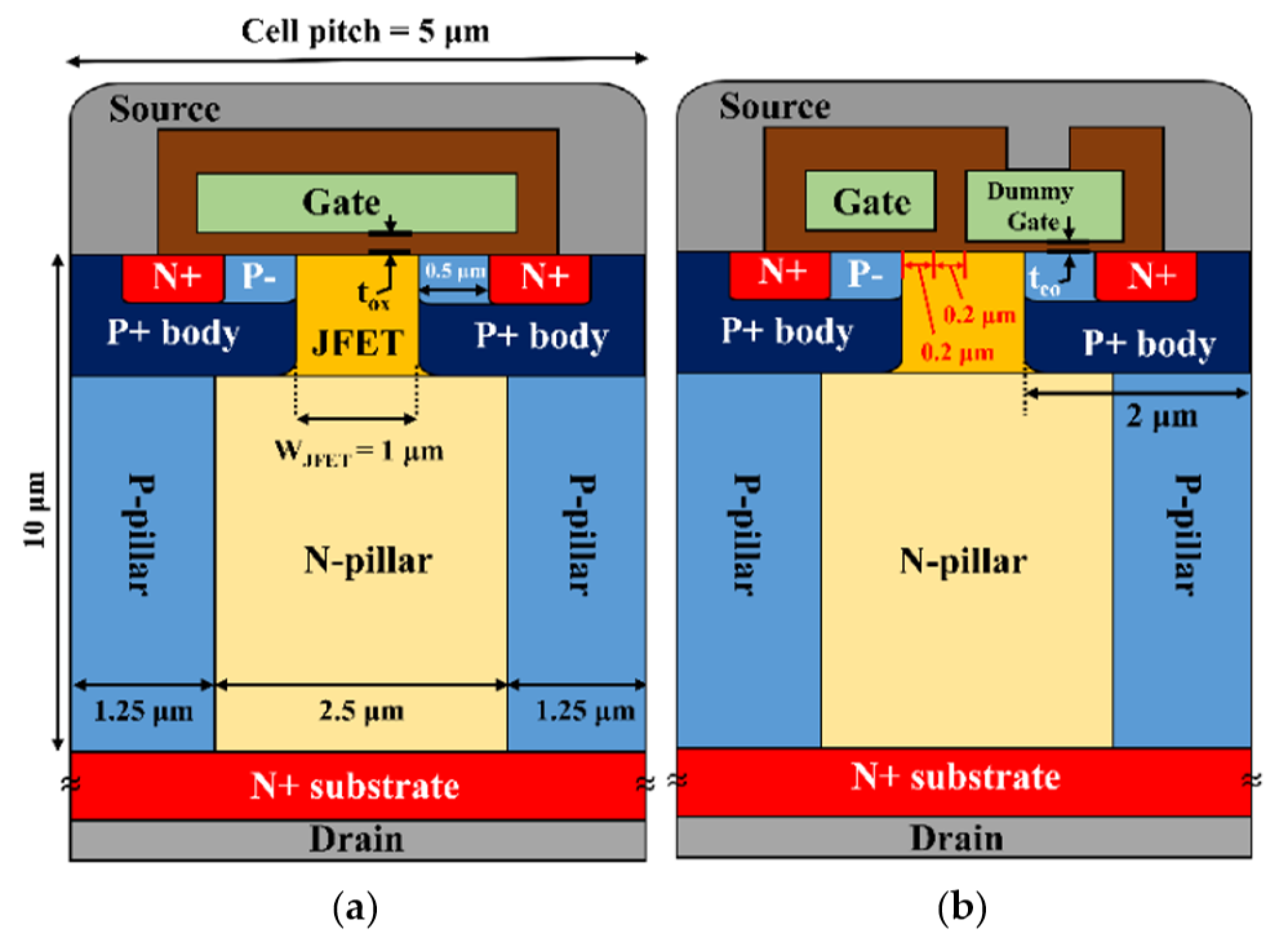
2. Device Structures and Simulation Background

The physical models used in the Sentaurus TCAD simulation contain bandgap narrowing (BGN) and Fermi–Dirac statistics. The recombination models contain Auger, Shockley–Read–Hall (SRH), the doping-dependent model and the temperature-dependent model [23]. The incomplete ionization and Hatakeyama avalanche models are also included. The mobility model contained the doping-dependent Arora model, Enormal and high field saturation. The anisotropic behavior in mobility and temperature characteristics of the SiC are also taken into consideration. A fixed charge concentration of 1 × 1012 cm–2 was included at the SiC/SiO2 interface for all of the devices [24]. For electro-thermal mixed-mode simulation in short circuit characteristics, the thermodynamic model and analytic TEPower model are considered to describe self-heating effects and thermoelectric powers in nondegenerate semiconductors [25].
Figure 1 represents the schematic cross-sectional views and dimension parameters of the SJ-MOSFET and MCD SJ-MOSFET. The doping and dimension parameters of the two devices refer to published work [20]. Both devices feature the same doping and dimension parameters, except for the gate structure. The active gate extends over the P-base region, set to 0.2 μm in our proposed device. The doping concentration of the JFET region in both structures is set 1 × 1017 cm–3 to reduce the RON. The body region of SiC MOSFET should be well designed because it has great influence not only on device performance, but also on device reliability [26]. We adopted shielded planar topology in this study, which features a P+ body region under the channel region [27]. Several studies have shown that the P+ region below the channel improves the short circuit capability of the device [25,28]. To obtain the charge balancing effect, the width of the P-pillar was set to 1.25 μm to occupy half of the cell pitch (5 μm), and it had the same doping concentration as that of the N-pillar. Figure 2 shows the influence of the pillar doping concentration on static characteristics in MCD SJ-MOSFET. In this study, we set the doping concentration of both pillar regions at 3.75 × 1016 cm–3, which achieves the highest Baliga’s figure of merit (BFOM = BV2/RON).
The dummy gate electrically connected to the source electrode features thinner channel diode oxide thickness (tco) than the active gate oxide thickness (tox = 50 nm), which acts as a channel diode. Figure 3a shows the influence of tco on the reverse conduction characteristics of the MCD SJ-MOSFET in the third quadrant with comparison to the SJ-MOSFET. The result clearly shows that a smaller tco leads to a faster turn-on in the proposed device because of the decreasing threshold voltage (VTH) of the MCD. However, since the thinner tco increases EMOX, the trade-off between VF and EMOX must be discussed. Figure 4a shows the EMOX and VF relationship of MCD SJ-MOSFET according to the change in tco. To meet the 3 MV/cm oxide reliability limit, tco = 10 nm was chosen for the MCD SJ-MOSFET with an EMOX of 2.95 MV/cm, as shown in Figure 4b. It seems that owing to the electric field shielding effect of the P+ body and the P-pillar, the electric field near the oxide can be effectively suppressed and the tco can be very thin. The VF of the proposed structure was 1.43 V, which was a similar level to that of the SBD-embedded SiC MOSFET [24,29]. The hole density distribution at IDS = −100 A/cm2 and VGS = −5 V for both devices is shown in Figure 3b,c, respectively. In MCD SJ-MOSFET, minority carrier injection was greatly suppressed in the JFET and the N-pillar region, which means deactivation of the parasitic body diode. Therefore, the MCD SJ-MOSFET can prevent the bipolar degradation issue caused by the body diode [30]. The detailed device parameters of both structures are listed in Table 1.
The proposed device could be fabricated in a similar way compared to the SJ-MOSFET. Only one additional mask is required to form the stepped oxide, and the separation of the dummy gate and the active gate can be performed simultaneously in the subsequent etching process after N+ polysilicon deposition [17,20]. Additionally, the source contact hole etching process of the dummy gate can be performed simultaneously in the ohmic contact hole etching process.

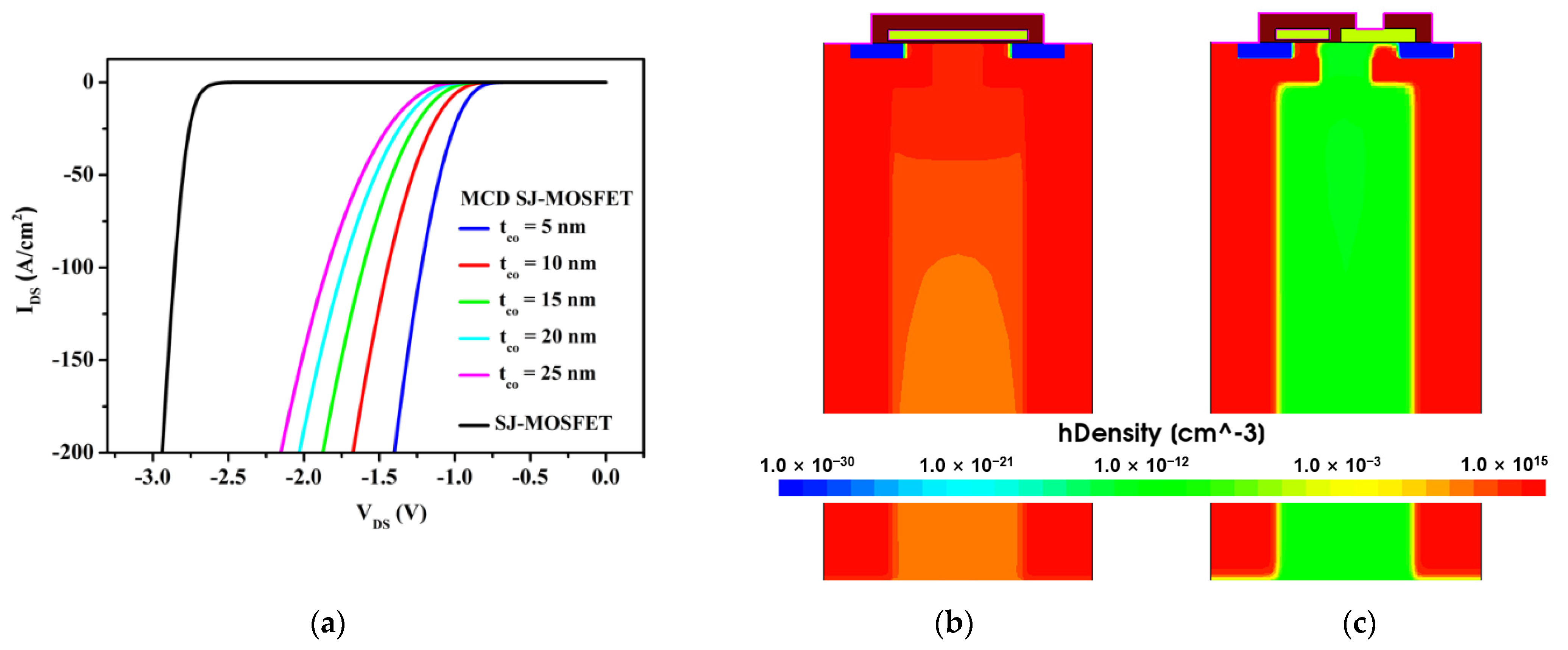
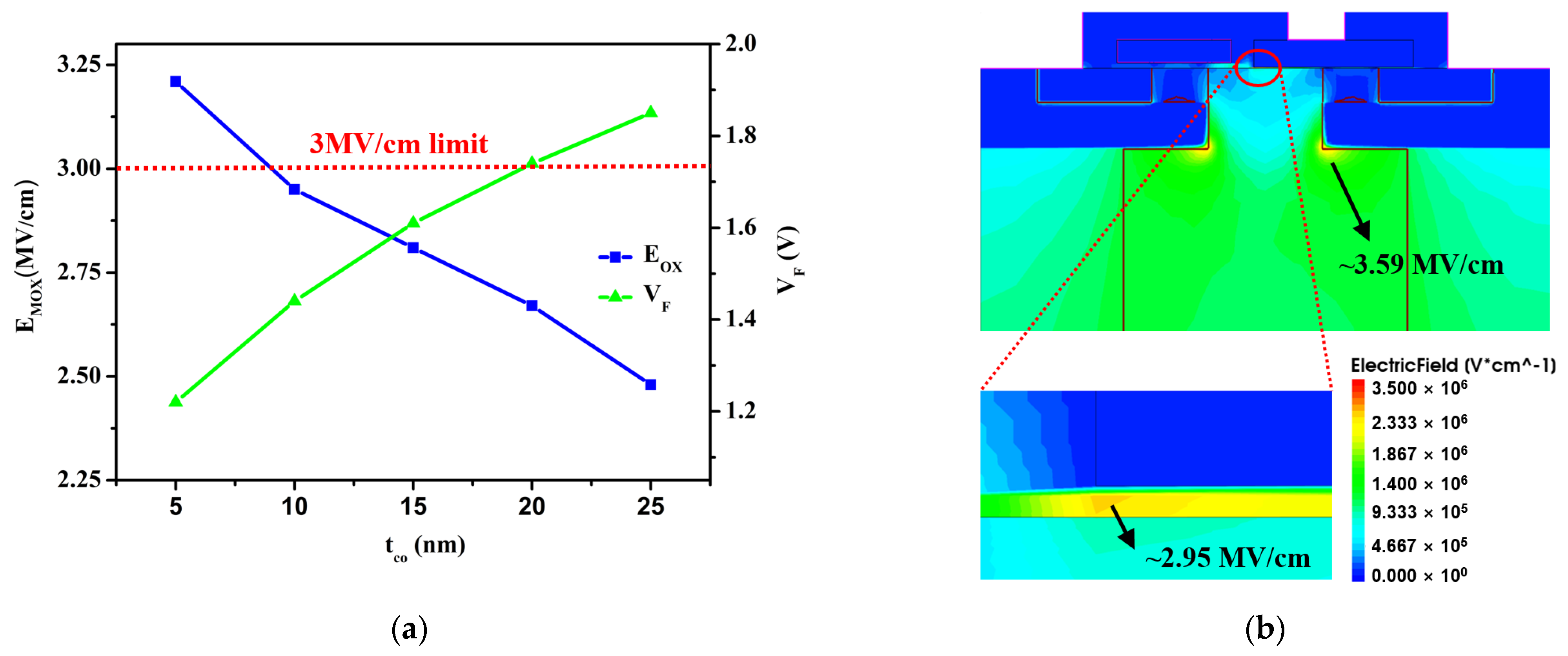
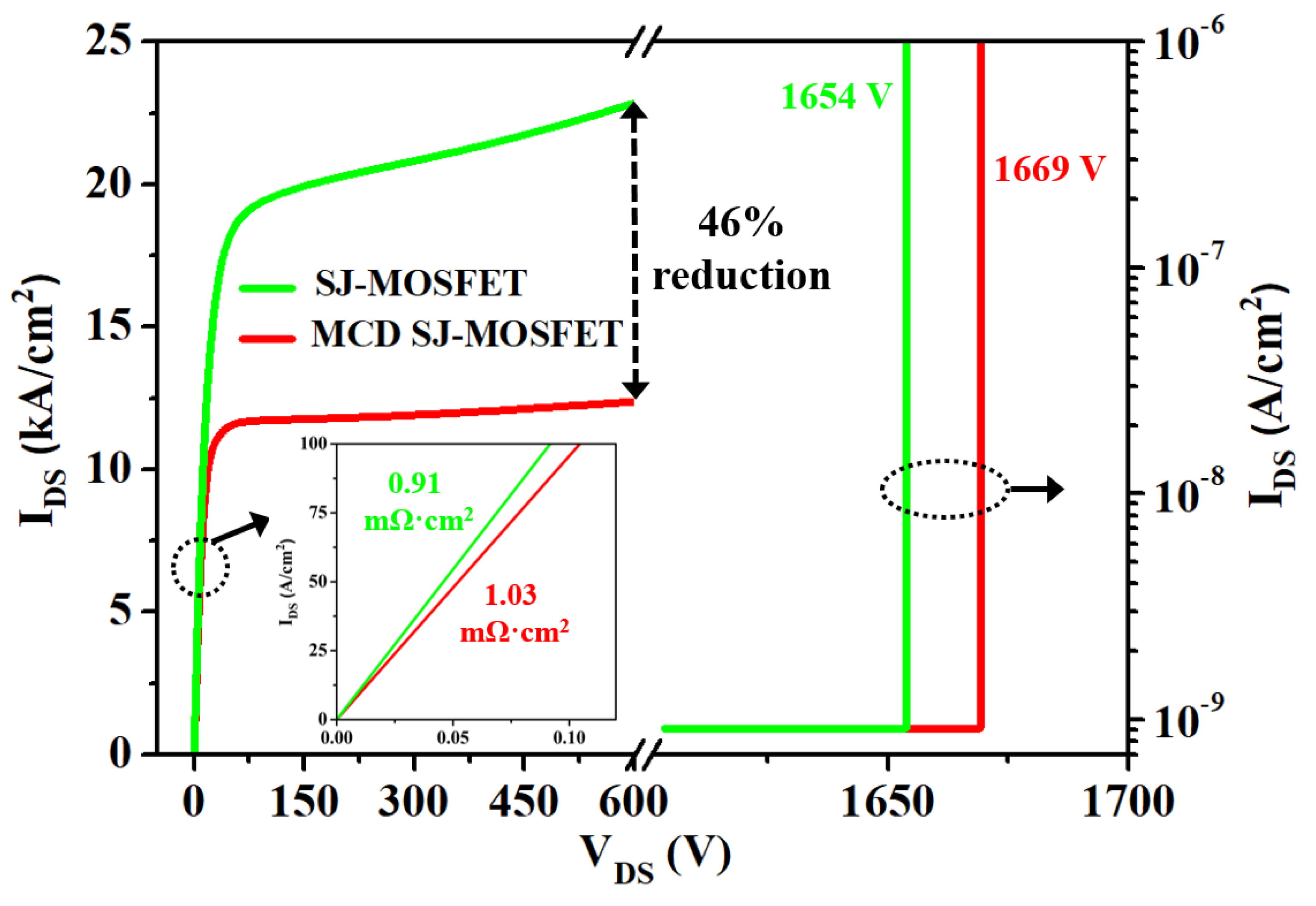
3. Results and Discussion

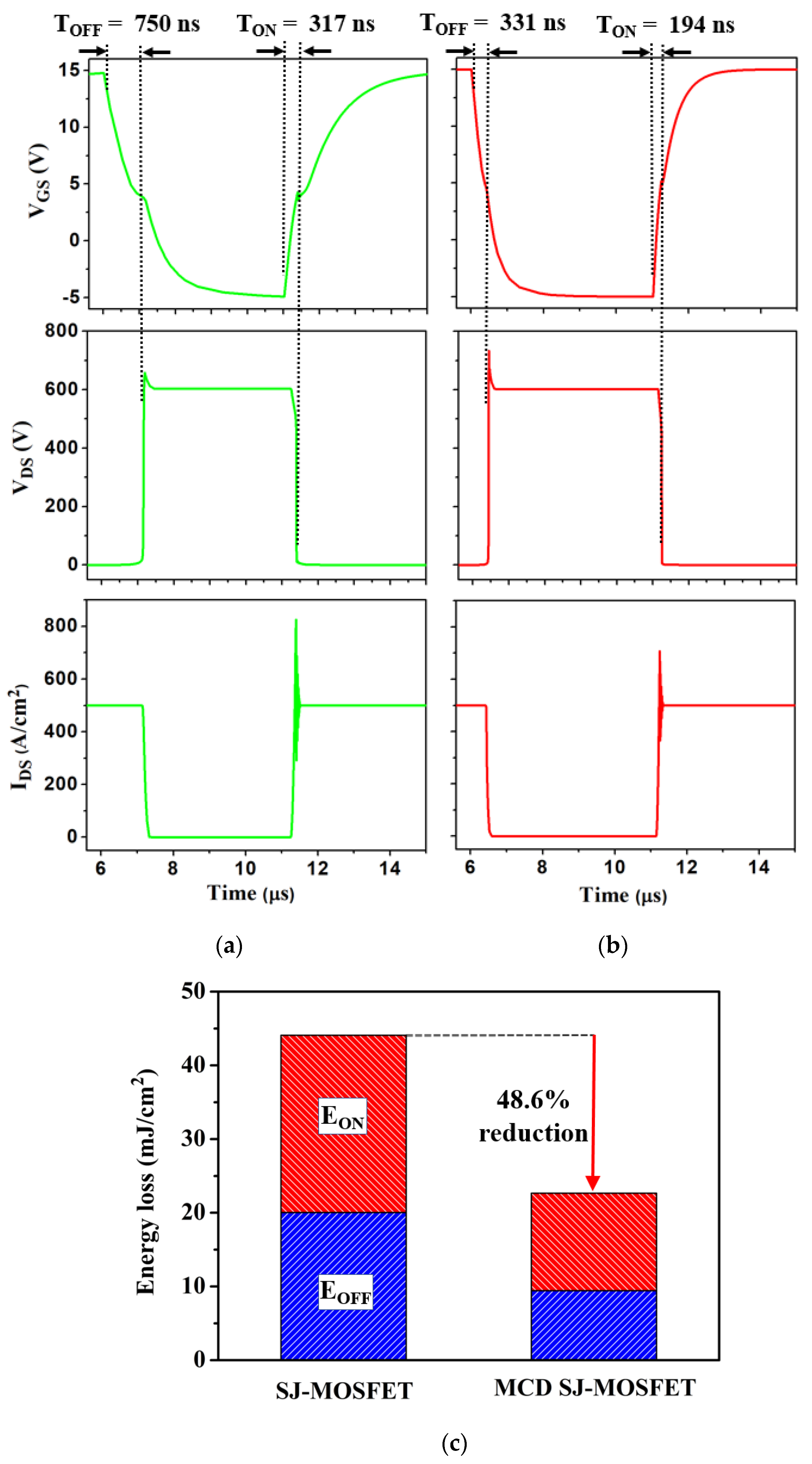
3.1. Electrical Characteristics

Figure 5 represents the I–V characteristics of both devices. In this study, BV was obtained at VGS = 0 V and IDS = 1 μA/cm2 and RON was obtained at VGS = 15 V and IDS = 100 A/cm2. The MCD SJ-MOSFET has a slightly higher RON (1.03 mΩ·cm2) than the SJ-MOSFET (0.91 mΩ·cm2), because current flows through only one active gate. However, it still achieved low RON level due to the high concentration of JFET region and SJ structure. It can be seen that the proposed structure has about 46% lower saturation current at VDS = 600 V compared to the SJ-MOSFET. Since the short circuit withstand time (tSC) and saturation current are usually inversely proportional, it is very helpful for short circuit characteristics [31]. The proposed device has slightly higher BV (1669 V) than the SJ-MOSFET (1654 V), given that the electric field was concentrated on the dummy gate, owing to its thin tco.
Figure 6a compares the reverse recovery characteristics of both devices. Additionally, the double pulse test circuit used in reverse recovery simulation is shown in Figure 6b. The lower arm MOSFET is used as a switch and the upper arm MOSFET is the actual device under test (DUT). The stray inductance and the gate resistance are 10 nH and 20 Ω, respectively. The load current is set to 500 A/cm2 and the drain bias is set to 600 V. In order to make the channel turn off and act as a diode mode, VGS = −5 V was applied in DUT. The results show that the peak reverse recovery current IRRM of the MCD SJ-MOSFET is 206 A/cm2, which is much lower than that of SJ-MOSFET (324 A/cm2). In addition, the reverse recovery time (trr) and the reverse recovery charge (Qrr) were improved by 43% and 59%, respectively, compared to the SJ-MOSFET. Here, the Qrr is defined in the following equation:
Q rr = 0 t rr I DS dt
where trr is defined as the time from when the reverse recovery current crosses zero to the time when the reverse recovery current drops down to 10% of the IRRM. Figure 7 compares the C–V characteristics of both devices. In the MCD SJ-MOSFET, the input capacitance (CISS = CGS + CGD) decreased by 46% due to the reduced active gate area when VDS = 600 V. Moreover, the CGD of the MCD SJ-MOSFET is greatly reduced (79%) when VDS = 600 V because of the reduced active gate area and depletion region capacitance caused by source-contacted dummy gate [32]. A comprehensive comparison of the device characteristics is shown in Table 2. Although BFOM is slightly decreased by 10%, it can be seen that the MCD SJ-MOSFET significantly improved the figures of merit RON × CGD by a factor of 4.3 compared to the SJ-MOSFET. As a result, these improvements indicate that the MCD SJ-MOSFET is more suitable for high-frequency applications.
Thereafter, the switching performance analysis of both devices was conducted using double pulse test circuit in Figure 6b. The lower arm MOSFET was the actual DUT and the body diode of the DUT (i.e., upper arm MOSFET) was used as a freewheeling diode. Figure 8a,b show the switching waveforms of both devices. Due to the large reduction in CISS and CGD, the MCD SJ-MOSFET has a short miller plateau region and a large dVGS/dt. As a result, the turn-off time (TOFF = from 90% of VGS to 90% of VDS) and the turn-on time (TON = from 10% of VGS to 10% of VDS) of the proposed device is reduced by 56% and 39%, respectively, compared to the SJ-MOSFET. It seems that the overshoot current of the MCD SJ-MOSFET is much lower than that of SJ-MOSFET because of the large reduction in the reverse recovery charge of the upper arm MOSFET [24]. This will further decrease the turn-on switching energy loss (EON). Figure 8c compares the switching energy loss of both devices. EON and EOFF are given by the following equations:
E ON = 0 T ON V DS · I DS dt
E OFF = 0 T OFF V DS · I DS dt
Owing to the faster switching time and enhanced reverse recovery characteristics, the switching energy loss (ESW = EON + EOFF) of the proposed device is improved by 48.6% compared to SJ-MOSFET. The detailed switching characteristics are summarized in Table 3.

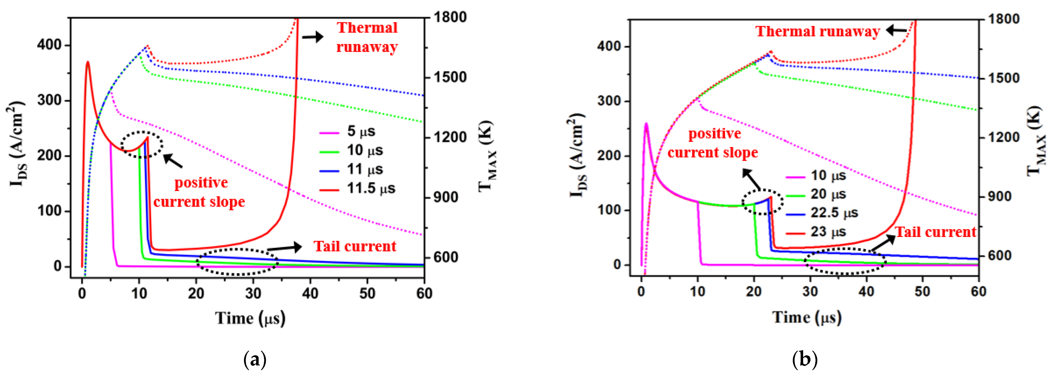
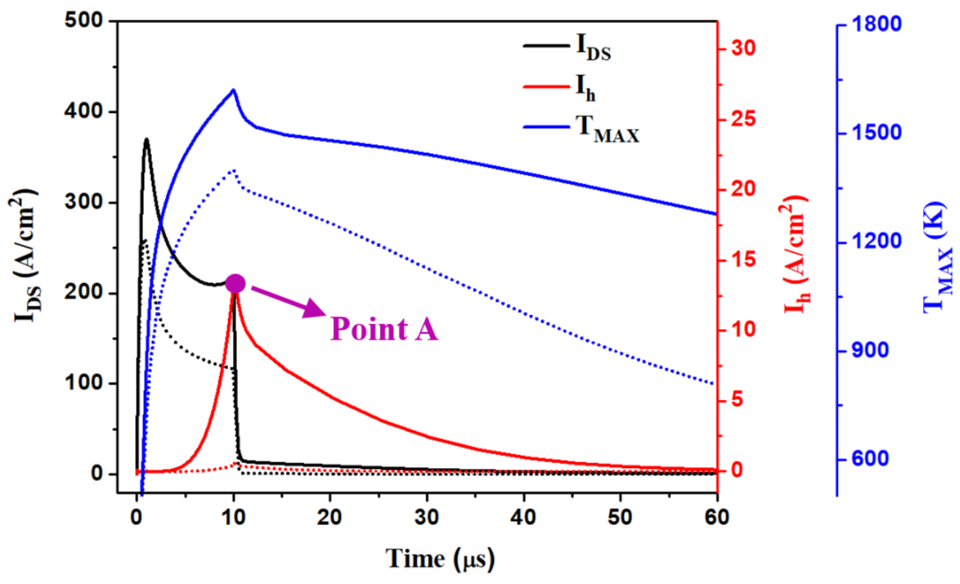
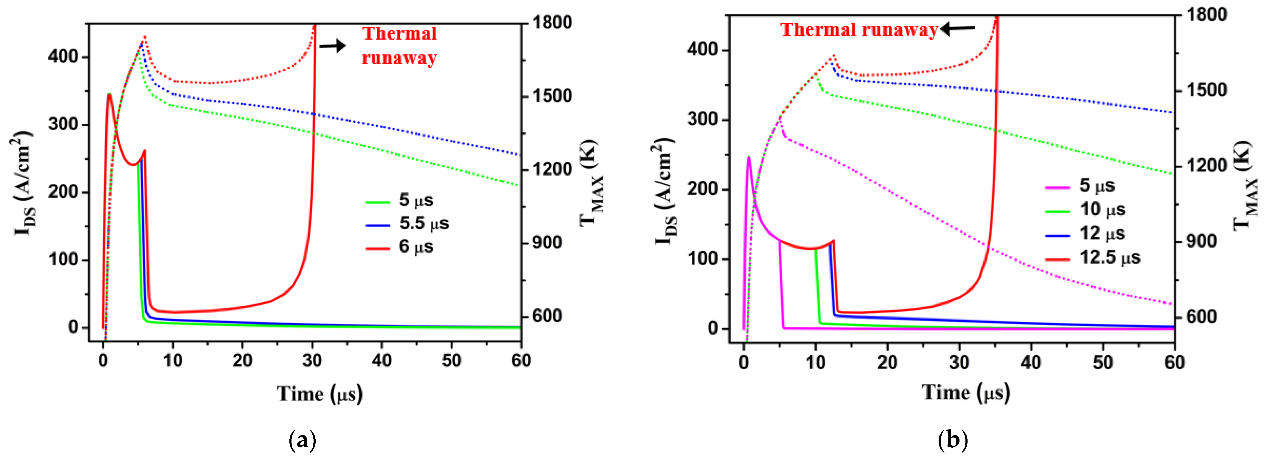
3.2. Short Circuit Characteristics

Short circuit ruggedness is one of the most crucial reliability issues in SiC MOSFETs because high voltage and high current are applied to the small cell area, resulting in high power dissipation [33,34]. Therefore, SiC MOSFETs with improved short circuit characteristics are essential. In this section, short circuit characteristics of both devices are investigated by means of electro-thermal mixed-mode TCAD simulation. The test circuit schematic is shown in Figure 9. The turn-on and turn-off gate voltage are set to 15 and 0 V, respectively, while the DC bus ranges from 400 to 600 V. The external gate resistance (RG) is 10 Ω.
Figure 10 shows the short circuit current and the maximum temperature (TMAX) waveforms of both devices with different pulse widths at a low drain bias (VDD = 400 V). Here, TMAX means the highest temperature in the device during short circuit simulation. Notably, two unique characteristics can be found in the short circuit current waveforms; the positive slope of the short circuit current at the end of the pulse and the increasing tail current with longer pulse width at turn-off state. This phenomenon is caused by leakage current at the PN junction due to the extremely high temperature, and has already been reported in several studies [35,36,37]. The tSC of the MCD SJ-MOSFET is 22.5 μs, which is about two times longer than that of the SJ-MOSFET (11 μs). The energy dissipation during the short circuit state (ESC) is defined as:
E SC = 0 t SC V DS · I DS dt
The ESC values were 1.05 and 1.16 J/cm2 for the SJ-MOSFET and MCD SJ-MOSFET, respectively.
Figure 11 compares both devices at the same pulse of 10 μs, with the MCD SJ-MOSFET at VDD = 400 V (the dotted line is TMAX and the solid line is IDS). Both the short circuit current and the TMAX of the MCD SJ-MOSFET are greatly reduced compared to the SJ-MOSFET. For a detailed understanding of the enhanced short-circuit characteristics of the MCD SJ-MOSFET, the simulated distribution of the electron current density, electric field, lattice temperature, and hole density at point A is shown in Figure 12. Generally, the joule heating equation is expressed as follows [38]:
q j = J · E
where qj is the joule heating energy density, J is the current density and E is the electric field. Although the electric field distribution is almost same in both structures, the joule heating energy density of the proposed structure becomes smaller due to the much lower current density. It can be confirmed that the lattice temperature of the SJ-MOSFET is much higher due to the increased joule heating energy density. The highest temperature region (hot spot) of the two devices is widely distributed between the P-pillars rather than being concentrated in the JFET region, as in conventional SiC MOSFETs (i.e., non SJ devices) [35]. This is because of the SJ structure in which the electric field is distributed vertically [39]. Therefore, the hot spot is far away from the gate oxide and source metal region, resulting in high reliability. Additionally, the SJ-MOSFET features a higher hole current (Ih) than the MCD SJ-MOSFET due to the high temperature, as shown in the red line in Figure 11. This explains the high tail current of the SJ-MOSFET, and it can be confirmed that Ih mainly formed at the high temperature region as shown in Figure 12. If the pulse width is further increased where Ih is large enough to activate the parasitic BJT, the drain current rises rapidly and thermal runaway occurs [25].
Finally, further investigation of the short circuit characteristics in high DC bus is conducted in a similar way. Figure 13 shows the short circuit current and the maximum temperature (TMAX) waveforms of both devices with different pulse widths at a high drain bias (VDD = 600 V). The tSC and ESC were 5.5 μs and 0.86 J/cm2 for the SJ-MOSFET and 12 μs and 0.98 J/cm2 for the MCD SJ-MOSFET, respectively. The MCD SJ-MOSFET showed a tSC more than two times higher and an improved ESC compared to the SJ-MOSFET, even at 600 V. It can be seen that the tSC and ESC of both devices are smaller than in the case of low drain bias. This is due to the elevated lattice temperature resulting from the high electric field, which was reported in a previous study [40]. The short circuit characteristics of both devices are summarized in Table 4.

4. Conclusions

In this study, a novel MCD SJ-MOSFET was developed and analyzed based on numerical TCAD simulations. Because of the P+ body and P-pillar region of the MCD SJ-MOSFET, the tco of the MCD can be set at a significantly lower level, while achieving a low EMOX of less than 3 MV/cm. Therefore, the proposed structure reduced VF by approximately half of that of the SJ-MOSFET, thus resulting in superior reverse recovery characteristics. In addition, the MCD SJ-MOSFET achieved a significantly lower CISS and CGD, thus resulting in significantly improved figures of merit RON × CGD when compared with the SJ-MOSFET. As a result, the proposed structure demonstrated a shorter switching time and reduced the ESW. Moreover, the simulation results revealed that the MCD SJ-MOSFET exhibited excellent short circuit characteristics in terms of the ESC and tSC. As a result, the MCD SJ-MOSFET is suitable for high-frequency and high-reliability applications.

Author Contributions

All authors contributed to this work. Investigation, J.Y. and K.K.; Methodology, J.Y. and K.K.; Supervision, J.Y. and K.K.; Writing—original draft, J.Y.; Writing—review and editing, K.K. All authors have read and agreed to the published version of the manuscript.

Funding

This research received no external funding.

Data Availability Statement

Data are not available on a publicly accessible repository and they cannot be shared under request.

Acknowledgments

This research was supported by the MSIT (Ministry of Science and ICT), Korea, under the ITRC (Information Technology Research Center) support program (IITP-2021-2018-0-01421) supervised by the IITP (Institute for Information and Communications Technology Promotion), and then Samsung Electronics.

Conflicts of Interest

The authors declare no conflict of interest.

References

  1. Deboy, G.; Marz, N.; Stengl, J.P.; Strack, H.A.S.H.; Tihanyi, J.A.T.J.; Weber, H.A.W.H. A new generation of high voltage MOSFETs breaks the limit line of silicon. In IEDM Tech; IEEE: San Francisco, CA, USA, 1998; pp. 683–685. [Google Scholar]
  2. Udrea, F.; Deboy, G.; Fujihira, T. Superjunction Power Devices, History, Development, and Future Prospects. IEEE Trans. Electron Devices 2017, 64, 713–727. [Google Scholar] [CrossRef]
  3. Masuda, T.; Saito, Y.; Kumazawa, T.; Hatayama, T.; Harada, S. 0.63 mΩ∙cm2/1170 V 4H-SiC Super Junction V-Groove Trench MOSFET; IEDM: San Francisco, CA, USA, 2018; pp. 8.1.1–8.1.4. [Google Scholar]
  4. Kosugi, R.; Sakuma, Y.; Kojima, K.; Itoh, S.; Nagata, A.; Yatsuo, T.; Tanaka, Y.; Okumura, H. First experimental demonstration of SiC super-junction (SJ) structure by multi-epitaxial growth method. In Proceedings of the IEEE 26th International Symposium on Power Semiconductor Devices & IC’s (ISPSD), Waikoloa, HI, USA, 15–19 June 2014; pp. 346–349. [Google Scholar]
  5. Zhong, X.; Wang, B.; Sheng, K. Design and experimental demonstration of 1.35 kV SiC super junction Schottky diode. In Proceedings of the 28th International Symposium on Power Semiconductor Devices and ICs (ISPSD), Prague, Czech Republic, 12–16 June 2016; pp. 231–234. [Google Scholar]
  6. Kosugi, R.; Ji, S.; Mochizuki, K.; Adachi, K.; Segawa, S.; Kawada, Y.; Yonezawa, Y.; Okumura, H. Breaking the Theoretical Limit of 6.5 kV-Class 4H-SiC Super-Junction (SJ) MOSFETs by Trench-Filling Epitaxial Growth. In Proceedings of the 31st International Symposium on Power Semiconductor Devices and ICs (ISPSD), Shanghai, China, 19–23 May 2019; pp. 39–42. [Google Scholar]
  7. Wang, H.; Wang, C.; Wang, B.; Ren, N.; Sheng, K. 4H-SiC Super-Junction JFET: Design and Experimental Demonstration. IEEE Electron Device Lett. 2020, 41, 445–448. [Google Scholar] [CrossRef]
  8. Matsui, R.; Suzuki, D.; Tanimoto, Y.; Kitamura, M.; Kikuchihara, H.; Mattausch, H.J.; Miura-Mattausch, M. Modeling of reverse recovery effect for embedded diode in SJ MOSFET. In Proceedings of the IEEE International Conference on Electron Devices and Solid-State Circuits (EDSSC), Singapore, 1–4 June 2015; pp. 375–378. [Google Scholar]
  9. Conrad, M.; DeDoncker, R.W. Avoiding reverse recovery effects in super junction MOSFET based half-bridges. In Proceedings of the IEEE 6th International Symposium on Power Electronics for Distributed Generation Systems (PEDG), Aachen, Germany, 22–25 June 2015; pp. 1–5. [Google Scholar]
  10. Yamashita, N.; Murakami, N.; Yachi, T. Conduction power loss in MOSFET synchronous rectifier with parallel-connected Schottky barrier diode. IEEE Trans. Power Electron. 1998, 13, 667–673. [Google Scholar] [CrossRef]
  11. Vudumula, P.; Kotamraju, S. The reverse recovery characteristics of an SiC superjunction MOSFET with a p-type Schottky diode embedded at the drain side for improved reliability. J. Comput. Electron. 2021, 20, 1187–1195. [Google Scholar] [CrossRef]
  12. Kotamraju, S.; Vudumula, P. Improved reverse recovery characteristics obtained in 4H-SiC double-trench superjunction MOSFET with an integrated p-type Schottky diode. IET Circuits Devices Syst. 2020, 14, 1283–1288. [Google Scholar] [CrossRef]
  13. Zhang, Y.; Yang, X.; Chen, H.; Li, K.; Zhong, W.; Luo, M.; Luo, J.; Zhang, B.; Bai, S. Investigating the Failure Mechanism of Short-Circuit Tests in 1.2-kV SiC JBS-Integrated MOSFETs. IEEE Trans. Electron Devices 2020, 67, 4027–4032. [Google Scholar] [CrossRef]
  14. Okawa, M.; Aiba, R.; Kanamori, T.; Kobayashi, Y.; Harada, S.; Yano, H.; Iwamuro, N. First Demonstration of Short-Circuit Capability for a 1.2 kV SiC SWITCH-MOS. IEEE J. Electron Devices Soc. 2019, 7, 613–620. [Google Scholar] [CrossRef]
  15. Aiba, R.; Matsui, K.; Baba, M.; Harada, S.; Yano, H.; Iwamuro, N. Demonstration of Superior Electrical Characteristics for 1.2 kV SiC Schottky Barrier Diode-Wall Integrated Trench MOSFET with Higher Schottky Barrier Height Metal. IEEE Electron Device Lett. 2020, 41, 1810–1813. [Google Scholar] [CrossRef]
  16. Okawa, M.; Kanamori, T.; Aiba, R.; Yano, H.; Iwamuro, N.; Harada, S. Analysis of 1.2 kV SiC SWITCH-MOS after Short-circuit Stress. In Proceedings of the 32nd International Symposium on Power Semiconductor Devices and ICs (ISPSD), Vienna, Austria, 13–18 September 2020; pp. 74–77. [Google Scholar]
  17. Zhang, M.; Wei, J.; Zhou, X.; Jiang, H.; Li, B.; Chen, K.J. Simulation Study of a Power MOSFET with Built-in Channel Diode for Enhanced Reverse Recovery Performance. IEEE Electron Device Lett. 2019, 40, 79–82. [Google Scholar] [CrossRef]
  18. Li, P.; Guo, J.; Lin, Z.; Hu, S. A Power MOSFET with P-Base Schottky Diode and Built-In Channel Diode for Fast Reverse Recovery. IEEE J. Electron Devices Soc. 2021, 9, 300–305. [Google Scholar]
  19. Zhou, X.; Pang, H.; Jia, Y.; Hu, D.; Wu, Y.; Tang, Y.; Xia, T.; Gong, H.; Zhao, Y. SiC Double-Trench MOSFETs with Embedded MOS-Channel Diode. IEEE Trans. Electron Devices 2020, 67, 582–587. [Google Scholar] [CrossRef]
  20. Zhou, X.; Gong, H.; Jia, Y.; Hu, D.; Wu, Y.; Xia, T.; Pang, H.; Zhao, Y. SiC Planar MOSFETs With Built-In Reverse MOS-Channel Diode for Enhanced Performance. IEEE J. Electron Devices Soc. 2020, 8, 619–625. [Google Scholar] [CrossRef]
  21. Krishnaswami, S.; Das, M.; Hull, B.; Ryu, S.H.; Scofield, J.; Agarwal, A.; Palmour, J. Gate oxide reliability of 4H-SiC MOS devices, IEEE International Reliability Physics Symposium. In Proceedings of the 43rd Annual, San Jose, CA, USA, 17–21 April 2005; pp. 592–593. [Google Scholar]
  22. Ye, Z.Y.; Liu, L.; Yao, Y.; Lin, M.Z.; Wang, P.F. Fabrication of a 650V Superjunction MOSFET with Built-in MOS-Channel Diode for Fast Reverse Recovery. IEEE Electron Device Lett. 2019, 40, 1159–1162. [Google Scholar] [CrossRef]
  23. Synopsys Inc. Sentaurus Device Manual, User Manual, Version O-2016.06; Synopsys Inc.: Mountain View, CA, USA, 2016. [Google Scholar]
  24. Han, Z.; Bai, Y.; Chen, H.; Li, C.; Lu, J.; Song, G.; Liu, X. A trench/planar SiC MOSFET integrated with SBD (TPSBD) for low reverse recovery charge and low switching loss. Semicond. Sci. Technol. 2020, 35, 10. [Google Scholar] [CrossRef]
  25. Chen, X.; Chen, H.; Shi, B.; Wang, Y.; Li, X.; Zhou, C.; Li, C.; Deng, X.; Luo, H.; Wu, Y.; et al. Investigation on Short-Circuit Characterization and Optimization of 3.3-kV SiC MOSFETs. IEEE Trans. Electron Devices 2021, 68, 184–191. [Google Scholar] [CrossRef]
  26. Ni, W.; Wang, X.; Xu, M.; Li, M.; Feng, C.; Xiao, H.; Jiang, L.; Li, W.; Wang, Q. Comparative Study of SiC Planar MOSFETs with Different p-Body Designs. IEEE Trans. Electron Devices 2020, 67, 1071–1076. [Google Scholar] [CrossRef]
  27. Baliga, B.J. Advanced High Voltage Power Device Concepts, 1st ed.; Springer: Cham, Switzerland, 2011; pp. 481–489. [Google Scholar]
  28. Reigosa, P.D.; Schulz, N.; Minamisawa, R. Short-circuit robustness of retrograde channel doping 1.2 kV SiC MOSFETs. Microelectron. Reliab. 2021, 120, 114117. [Google Scholar] [CrossRef]
  29. Sung, W.; Baliga, B.J. On Developing One-Chip Integration of 1.2 kV SiC MOSFET and JBS Diode (JBSFET). IEEE Trans. Ind. Electron. 2017, 64, 8206–8212. [Google Scholar] [CrossRef]
  30. Ishigaki, T.; Hayakawa, S.; Murata, T.; Masuda, T.; Oda, T.; Takayanagi, Y. Diode-Less SiC Power Module with Countermeasures Against Bipolar Degradation to Achieve Ultrahigh Power Density. IEEE Trans. Electron Devices 2020, 67, 2035–2043. [Google Scholar] [CrossRef]
  31. Sampath, M.; Morisette, D.T.; Cooper, J.A. Constant-Gate-Charge Scaling for Increased Short-Circuit Withstand Time in SiC Power Devices. In Proceedings of the IEEE International Reliability Physics Symposium (IRPS), Dallas, TX, USA, 28 April–30 May 2020; pp. 1–4. [Google Scholar]
  32. Vudumula, P.; Kotamraju, S. Design and Optimization of 1.2-kV SiC Planar Inversion MOSFET Using Split Dummy Gate Concept for High-Frequency Applications. IEEE Trans. Electron Devices 2019, 66, 5266–5271. [Google Scholar] [CrossRef]
  33. Wei, J.; Liu, S.; Tong, J.; Zhang, X.; Sun, W.; Huang, A.Q. Understanding Short-Circuit Failure Mechanism of Double-Trench SiC Power MOSFETs. IEEE Trans. Electron Devices 2020, 67, 5593–5599. [Google Scholar] [CrossRef]
  34. Qin, H.; Dong, Y.; Xu, K.; Xu, H.; Fu, D.; Wang, S.; Zhao, C. A comprehensive study of the short-circuit characteristics of SiC MOSFETs. In Proceedings of the 12th IEEE Conference on Industrial Electronics and Applications (ICIEA), Siem Reap, Cambodia, 18–20 June 2017; pp. 332–336. [Google Scholar]
  35. Romano, G.; Fayyaz, A.; Riccio, M.; Maresca, L.; Breglio, G.; Castellazzi, A.; Irace, A. A Comprehensive Study of Short-Circuit Ruggedness of Silicon Carbide Power MOSFETs. IEEE J. Emerg. Sel. Top. Power Electron. 2016, 4, 978–987. [Google Scholar] [CrossRef]
  36. Castellazzi, A.; Fayyaz, A.; Yang, L.; Riccio, M.; Irace, A. Short-circuit robustness of SiC Power MOSFETs: Experimental analysis. In Proceedings of the IEEE 26th International Symposium on Power Semiconductor Devices & IC’s (ISPSD), Waikoloa, HI, USA, 15–19 June 2014; pp. 71–74. [Google Scholar]
  37. Kakarla, B.; Tsibizov, A.; Stark, R.; Badstübner, I.K.; Grossner, U. Short Circuit Robustness and Carrier Lifetime in Silicon Carbide MOSFETs. In Proceedings of the 32nd International Symposium on Power Semiconductor Devices and ICs (ISPSD), Vienna, Austria, 13–18 September 2020; pp. 234–237. [Google Scholar]
  38. Aikio, A.T.; Selkälä, A. Statistical properties of Joule heating rate, electric field and conductances at high latitudes. Ann. Geophys. 2009, 27, 2661–2673. [Google Scholar] [CrossRef] [Green Version]
  39. Okada, M.; Kyogoku, S.; Kumazawa, T.; Saito, J.; Morimoto, T.; Takei, M.; Harada, S. Superior Short-Circuit Performance of SiC Superjunction MOSFET. In Proceedings of the 32nd International Symposium on Power Semiconductor Devices and ICs (ISPSD), Vienna, Austria, 13–18 September 2020; pp. 70–73. [Google Scholar]
  40. Namai, M.; An, J.; Yano, H.; Iwamuro, N. Investigation of shoet-circuit failure mechanisms of SiC MOSFETs by varying DC bus voltage. Jpn. J. Appl. Phys. 2018, 57, 7. [Google Scholar] [CrossRef]
Figure 1. Schematic cross-sectional views of (a) SJ-MOSFET and (b) MCD SJ-MOSFET.
Electronics 10 02619 g001
Figure 2. Influence of the pillar doping concentration on static characteristics in the MCD SJ-MOSFET. RON is obtained at VGS = 15 V and IDS = 100 A/cm2. BV is obtained at VGS = 0 V and IDS = 1 μA/cm2.
Electronics 10 02619 g002
Figure 3. (a) Influence of tco on the reverse conduction characteristics in the MCD SJ-MOSFET in comparison to the SJ-MOSFET at VGS = −5 V. Hole density distribution at IDS = −100 A/cm2 and VGS = −5 V for the (b) SJ-MOSFET and (c) MCD SJ-MOSFET (when tco = 10 nm).
Electronics 10 02619 g003
Figure 4. (a) Maximum oxide electric field (EMOX) and turn-on voltage (VF) changes of the MCD SJ-MOSFET according to the change tco, (b) electric field distributions of the MCD SJ-MOSFET (when tco = 10 nm).
Electronics 10 02619 g004
Figure 5. I–V characteristics of both devices. The output characteristics are obtained at VGS = 15 V and the blocking characteristics are obtained when VGS = 0 V.
Electronics 10 02619 g005
Figure 6. (a) Reverse recovery characteristics of both devices, (b) Double pulse test circuit used in reverse recovery simulation. The active area of the device under test (DUT) and lower arm MOSFET is 1 cm2.
Electronics 10 02619 g006
Figure 7. C–V characteristics of the SJ-MOSFET and MCD SJ-MOSFET. When VGS = 0 V, AC signal of 1 MHz.
Electronics 10 02619 g007
Figure 8. Switching waveforms of the (a) SJ-MOSFET and (b) MCD SJ-MOSFET. (c) Switching energy loss diagrams of both devices.
Electronics 10 02619 g008
Figure 9. Short circuit simulation schematic.
Electronics 10 02619 g009
Figure 10. Simulated short circuit current and maximum temperature (TMAX) waveforms of the (a) SJ-MOSFET and (b) MCD SJ-MOSFET at VDD = 400 V (the dotted line is TMAX and the solid line is IDS).
Electronics 10 02619 g010
Figure 11. Comparison of short circuit characteristics at VDD = 400 V, and a pulse width of 10 μs (the dotted line refers to the MCD SJ-MOSFET, and the solid line refers to the SJ-MOSFET).
Electronics 10 02619 g011
Figure 12. Simulated distribution of electron current density, electric field, lattice temperature, and hole density at point A.
Electronics 10 02619 g012
Figure 13. Simulated short circuit current and maximum temperature waveforms of the (a) SJ-MOSFET and the (b) MCD SJ-MOSFET at VDD = 600 V (the dotted line is TMAX and the solid line is IDS).
Electronics 10 02619 g013
Table 1. Device parameters for TCAD simulation.
ParameterSJ-MCD-
Drift layer thickness (μm)1010
N-pillar/P-pillar doping (cm−3)3.75 × 10163.75 × 1016
JFET doping (cm−3)1 × 10171 × 1017
Channel length (μm)0.50.5
N+ substrate thickness (μm)100100
N+ substrate doping (cm−3)1 × 10191 × 1019
Channel doping (cm−3)1 × 10171 × 1017
P+ body doping (cm−3) 5 × 10185 × 1018
N+ source doping (cm−3)1 × 10191 × 1019
EFP region doping (cm−3)5 × 10185 × 1018
Width of P-pillar (μm)1.251.25
Cell pitch (μm)55
Width of JFET (μm)11
tox (nm)5050
tco (nm)-10
Distance of the active gate extend over the channel (μm)-0.2
Table 2. Comparison of device characteristics.
SJ-MCD-Unit
VF2.861.43V
1 BV16541669V
2 RON0.911.03mΩ·cm2
BFOM30062704MW/cm2
3 CISS27.114.5nF/cm2
3 CGD21.24.4pF/cm2
RON × CGD19.34.5mΩ∙pF
IRRM324206A/cm2
trr4425ns
Qrr72702999nC/cm2
1 BV was obtained at VGS = 0 V and IDS = 1 μA/cm2. 2 RON was obtained at VGS = 15 V and IDS = 100 A/cm2. 3 CISS and CGD were obtained at VDS = 600 V.
Table 3. Comparison of device characteristics.
SJ-MCD-Unit
TOFF750331ns
TON317194ns
EOFF20.039.43mJ/cm2
EON24.0513.24mJ/cm2
ESW44.0822.67mJ/cm2
Table 4. Comparison of short circuit characteristics.
SJ-MCD-Unit
tSC (@VDD = 400 V)1122.5μs
tSC (@VDD = 600 V)5.512μs
ESC (@VDD = 400 V)1.051.16J/cm2
ESC (@VDD = 600 V)0.860.98J/cm2
Publisher’s Note: MDPI stays neutral with regard to jurisdictional claims in published maps and institutional affiliations.

