
Novel Bio-Optoelectronics Enabled by Flexible Micro Light-Emitting Diodes


Abstract
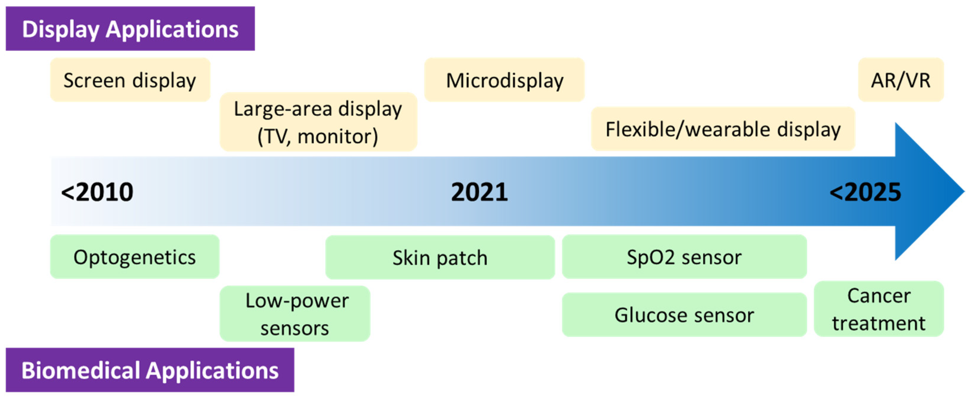
:1. Introduction
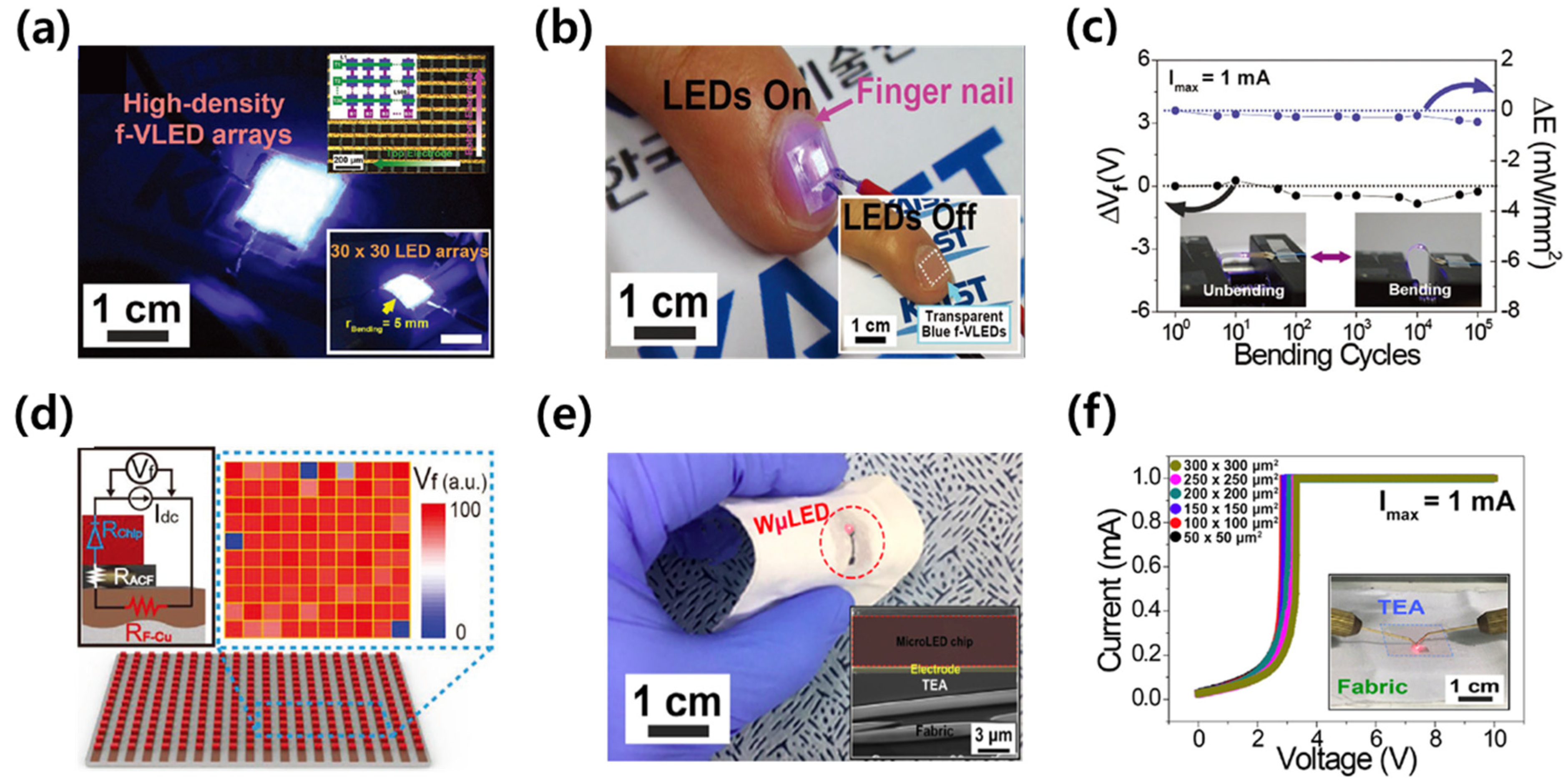
2. Flexible Micro Light-Emitting Diodes
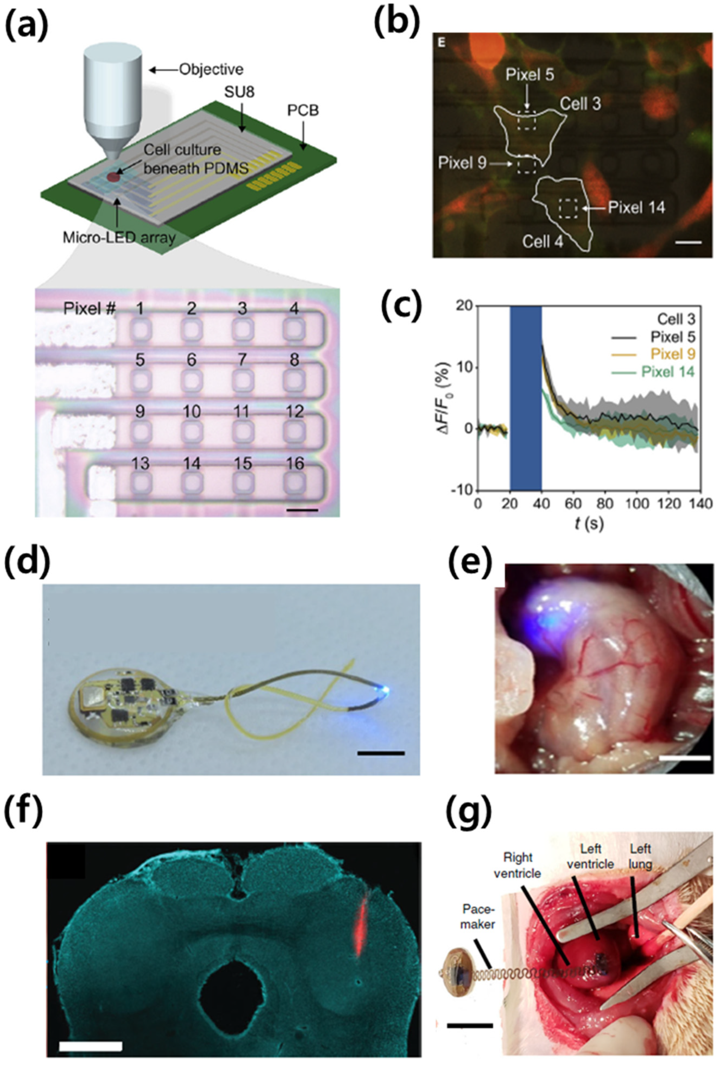
3. Optogenetic Stimulators
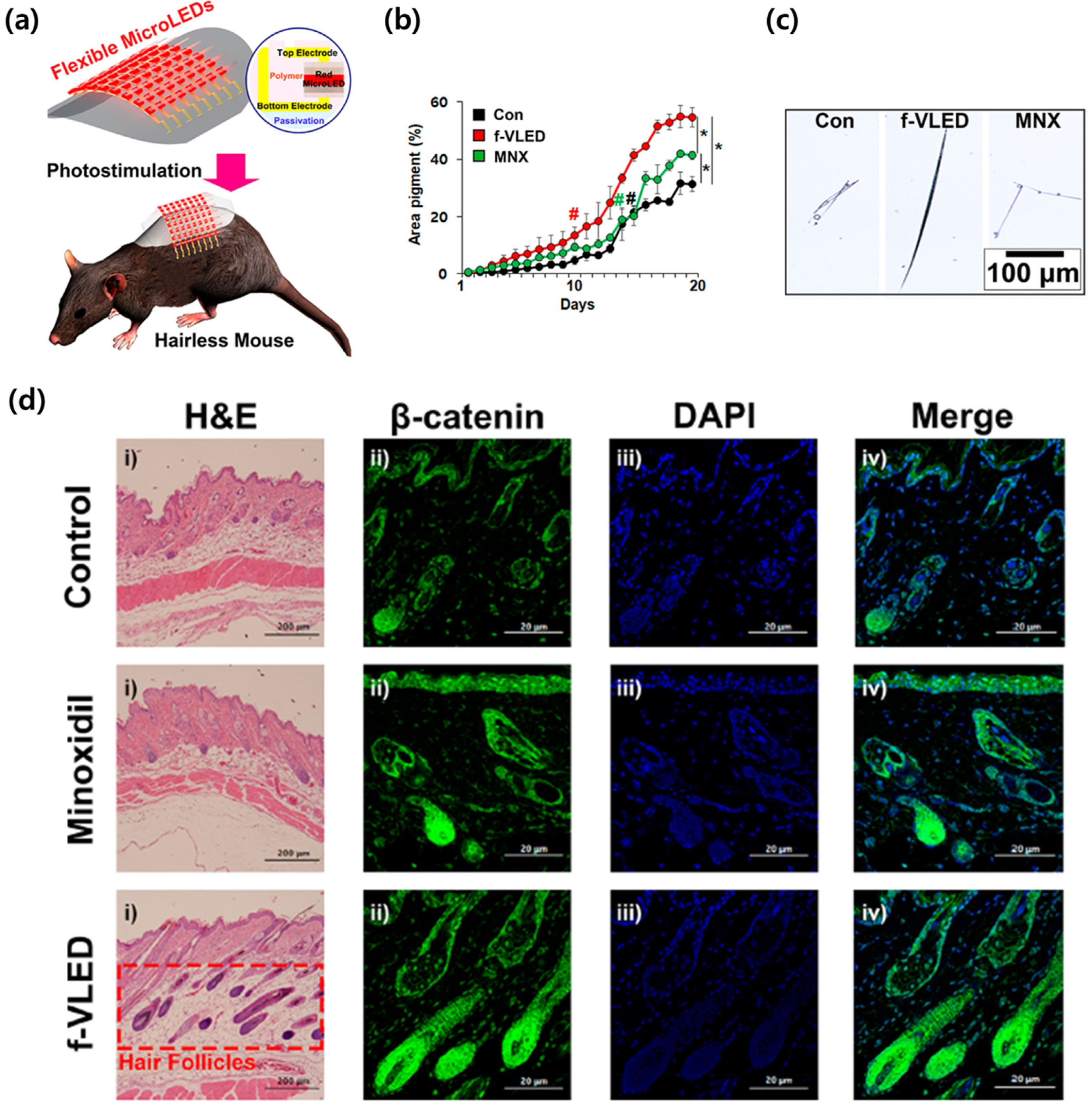
4. Other Biomedical Applications
5. Conclusions
Funding
Conflicts of Interest
References
- Lee, H.E.; Park, J.H.; Kim, T.J.; Im, D.; Shin, J.H.; Kim, D.H.; Mohammad, B.; Kang, I.-S.; Lee, K.J. Novel Electronics for Flexible and Neuromorphic Computing. Adv. Funct. Mater. 2018, 28, 1801690. [Google Scholar] [CrossRef]
- Joe, D.J.; Kim, S.; Park, J.H.; Park, D.Y.; Lee, H.E.; Im, T.H.; Choi, I.; Ruoff, R.S.; Lee, K.J. Laser-Material Interactions for Flexible Applications. Adv. Mater. 2017, 29, 1606586. [Google Scholar] [CrossRef]
- Kim, S.J.; Lee, H.E.; Choi, H.; Kim, Y.; We, J.H.; Shin, J.S.; Lee, K.J.; Cho, B.J. High-Performance Flexible Thermoelectric Power Generator Using Laser Multiscanning Lift-Off Process. ACS Nano 2016, 10, 10851–10857. [Google Scholar] [CrossRef] [PubMed]
- Lee, H.; Lee, H.E.; Wang, H.S.; Kang, S.; Lee, D.; Kim, Y.H.; Shin, J.H.; Lim, Y.; Lee, K.J.; Bae, B. Hierarchically Surface-Textured Ultrastable Hybrid Film for Large-Scale Triboelectric Nanogenerators. Adv. Funct. Mater. 2020, 30, 2005610. [Google Scholar] [CrossRef]
- Im, T.H.; Lee, C.H.; Kim, J.C.; Kim, S.; Kim, M.; Park, C.M.; Lee, H.E.; Park, J.H.; Jang, M.S.; Lee, D.C.; et al. Metastable quantum dot for photoelectric devices via flash-induced one-step sequential self-formation. Nano Energy 2021, 84, 105889. [Google Scholar] [CrossRef]
- Wang, H.S.; Im, T.H.; Kim, Y.B.; Sung, S.H.; Min, S.; Park, S.H.; Lee, H.E.; Jeong, C.K.; Park, J.H.; Lee, K.J. Flash-welded ultraflat silver nanowire network for flexible organic light-emitting diode and triboelectric tactile sensor. APL Mater. 2021, 9, 061112. [Google Scholar] [CrossRef]
- Lee, H.E.; Shin, J.H.; Lee, S.H.; Lee, J.H.; Park, S.H.; Lee, K.J. Flexible micro light-emitting diodes for wearable applications. In Proceedings of the Light-Emitting Devices, Materials, and Applications, San Francisco, CA, USA, 1 March 2019; Strassburg, M., Kim, J.K., Krames, M.R., Eds.; SPIE: San Francisco, CA, USA, 2019; p. 14. [Google Scholar]
- Kim, S.J.; Choi, H.; Kim, Y.; We, J.H.; Shin, J.S.; Lee, H.E.; Oh, M.-W.; Lee, K.J.; Cho, B.J. Post ionized defect engineering of the screen-printed Bi 2 Te 2.7 Se 0.3 thick film for high performance flexible thermoelectric generator. Nano Energy 2017, 31, 258–263. [Google Scholar] [CrossRef]
- Kim, D.H.; Lee, H.E.; You, B.K.; Cho, S.B.; Mishra, R.; Kang, I.; Lee, K.J. Flexible Crossbar-Structured Phase Change Memory Array via Mo-Based Interfacial Physical Lift-Off. Adv. Funct. Mater. 2019, 29, 1806338. [Google Scholar] [CrossRef]
- Lee, H.E.; Shin, J.H.; Park, J.H.; Hong, S.K.; Park, S.H.; Lee, S.H.; Lee, J.H.; Kang, I.; Lee, K.J. Micro Light-Emitting Diodes for Display and Flexible Biomedical Applications. Adv. Funct. Mater. 2019, 29, 1808075. [Google Scholar] [CrossRef]
- Park, J.H.; Lee, H.E.; Jeong, C.K.; Kim, D.H.; Hong, S.K.; Park, K.-I.; Lee, K.J. Self-powered flexible electronics beyond thermal limits. Nano Energy 2019, 56, 531–546. [Google Scholar] [CrossRef]
- Jung, D.H.; Park, J.H.; Lee, H.E.; Byun, J.; Im, T.H.; Lee, G.Y.; Seok, J.Y.; Yun, T.; Lee, K.J.; Kim, S.O. Flash-induced ultrafast recrystallization of perovskite for flexible light-emitting diodes. Nano Energy 2019, 61, 236–244. [Google Scholar] [CrossRef]
- Peng, Y.; Que, M.; Lee, H.E.; Bao, R.; Wang, X.; Lu, J.; Yuan, Z.; Li, X.; Tao, J.; Sun, J.; et al. Achieving high-resolution pressure mapping via flexible GaN/ ZnO nanowire LEDs array by piezo-phototronic effect. Nano Energy 2019, 58, 633–640. [Google Scholar] [CrossRef]
- Kim, I.H.; Im, T.H.; Lee, H.E.; Jang, J.; Wang, H.S.; Lee, G.Y.; Kim, I.; Lee, K.J.; Kim, S.O. Janus Graphene Liquid Crystalline Fiber with Tunable Properties Enabled by Ultrafast Flash Reduction. Small 2019, 15, 1901529. [Google Scholar] [CrossRef] [PubMed]
- Park, A.H.; Lee, S.H.; Lee, C.; Kim, J.; Lee, H.E.; Paik, S.-B.; Lee, K.J.; Kim, D. Optogenetic Mapping of Functional Connectivity in Freely Moving Mice via Insertable Wrapping Electrode Array Beneath the Skull. ACS Nano 2016, 10, 2791–2802. [Google Scholar] [CrossRef] [PubMed]
- Lee, H.E.; Kim, S.; Ko, J.; Yeom, H.-I.; Byun, C.-W.; Lee, S.H.; Joe, D.J.; Im, T.-H.; Park, S.-H.K.; Lee, K.J. Skin-Like Oxide Thin-Film Transistors for Transparent Displays. Adv. Funct. Mater. 2016, 26, 6170–6178. [Google Scholar] [CrossRef]
- Lee, H.E.; Park, J.H.; Jang, D.; Shin, J.H.; Im, T.H.; Lee, J.H.; Hong, S.K.; Wang, H.S.; Kwak, M.S.; Peddigari, M.; et al. Optogenetic brain neuromodulation by stray magnetic field via flash-enhanced magneto-mechano-triboelectric nanogenerator. Nano Energy 2020, 75, 104951. [Google Scholar] [CrossRef]
- Jeong, Y.; Lee, H.E.; Shin, A.; Kim, D.; Lee, K.J.; Kim, D. Progress in Brain-Compatible Interfaces with Soft Nanomaterials. Adv. Mater. 2020, 32, 1907522. [Google Scholar] [CrossRef] [PubMed]
- Park, J.H.; Seo, J.; Kim, C.; Joe, D.J.; Lee, H.E.; Im, T.H.; Seok, J.Y.; Jeong, C.K.; Ma, B.S.; Park, H.K.; et al. Flash-Induced Stretchable Cu Conductor via Multiscale-Interfacial Couplings. Adv. Sci. 2018, 5, 1801146. [Google Scholar] [CrossRef] [PubMed]
- Hwang, I.; Kim, H.N.; Seong, M.; Lee, S.-H.; Kang, M.; Yi, H.; Bae, W.G.; Kwak, M.K.; Jeong, H.E. Multifunctional Smart Skin Adhesive Patches for Advanced Health Care. Adv. Healthc. Mater. 2018, 7, 1800275. [Google Scholar] [CrossRef]
- Sreenilayam, S.P.; Ahad, I.U.; Nicolosi, V.; Acinas Garzon, V.; Brabazon, D. Advanced materials of printed wearables for physiological parameter monitoring. Mater. Today 2020, 32, 147–177. [Google Scholar] [CrossRef]
- Jin, H.; Abu-Raya, Y.S.; Haick, H. Advanced Materials for Health Monitoring with Skin-Based Wearable Devices. Adv. Healthc. Mater. 2017, 6, 1700024. [Google Scholar] [CrossRef] [PubMed]
- Lo, L.; Shi, H.; Wan, H.; Xu, Z.; Tan, X.; Wang, C. Inkjet-Printed Soft Resistive Pressure Sensor Patch for Wearable Electronics Applications. Adv. Mater. Technol. 2020, 5, 1900717. [Google Scholar] [CrossRef]
- Yang, J.C.; Mun, J.; Kwon, S.Y.; Park, S.; Bao, Z.; Park, S. Electronic Skin: Recent Progress and Future Prospects for Skin-Attachable Devices for Health Monitoring, Robotics, and Prosthetics. Adv. Mater. 2019, 31, 1904765. [Google Scholar] [CrossRef] [PubMed] [Green Version]
- Yeon, H.; Lee, H.; Kim, Y.; Lee, D.; Lee, Y.; Lee, J.S.; Shin, J.; Choi, C.; Kang, J.H.; Suh, J.M.; et al. Long-term reliable physical health monitoring by sweat pore–inspired perforated electronic skins. Sci. Adv. 2021, 7, 1–11. [Google Scholar] [CrossRef] [PubMed]
- Xi, D.; Xiao, M.; Cao, J.; Zhao, L.; Xu, N.; Long, S.; Fan, J.; Shao, K.; Sun, W.; Yan, X.; et al. NIR Light-Driving Barrier-Free Group Rotation in Nanoparticles with an 88.3% Photothermal Conversion Efficiency for Photothermal Therapy. Adv. Mater. 2020, 32, 1907855. [Google Scholar] [CrossRef]
- Xu, X.; Chen, J.; Cai, S.; Long, Z.; Zhang, Y.; Su, L.; He, S.; Tang, C.; Liu, P.; Peng, H.; et al. A Real-Time Wearable UV-Radiation Monitor based on a High-Performance p-CuZnS/n-TiO2 Photodetector. Adv. Mater. 2018, 30, 1803165. [Google Scholar] [CrossRef]
- Wang, C.; Xia, K.; Zhang, Y.; Kaplan, D.L. Silk-Based Advanced Materials for Soft Electronics. Acc. Chem. Res. 2019, 52, 2916–2927. [Google Scholar] [CrossRef]
- Zodrow, K.R.; Li, Q.; Buono, R.M.; Chen, W.; Daigger, G.; Dueñas-Osorio, L.; Elimelech, M.; Huang, X.; Jiang, G.; Kim, J.-H.; et al. Advanced Materials, Technologies, and Complex Systems Analyses: Emerging Opportunities to Enhance Urban Water Security. Environ. Sci. Technol. 2017, 51, 10274–10281. [Google Scholar] [CrossRef]
- Cai, S.; Xu, X.; Yang, W.; Chen, J.; Fang, X. Materials and Designs for Wearable Photodetectors. Adv. Mater. 2019, 31, 1808138. [Google Scholar] [CrossRef]
- Lee, H.E.; Choi, J.H.; Lee, S.H.; Jeong, M.; Shin, J.H.; Joe, D.J.; Kim, D.H.; Kim, C.W.; Park, J.H.; Lee, J.H.; et al. Monolithic Flexible Vertical GaN Light-Emitting Diodes for a Transparent Wireless Brain Optical Stimulator. Adv. Mater. 2018, 30, 1–10. [Google Scholar] [CrossRef]
- Jeong, C.K.; Park, K.-I.; Son, J.H.; Hwang, G.-T.; Lee, S.H.; Park, D.Y.; Lee, H.E.; Lee, H.K.; Byun, M.; Lee, K.J. Self-powered fully-flexible light-emitting system enabled by flexible energy harvester. Energy Environ. Sci. 2014, 7, 4035–4043. [Google Scholar] [CrossRef]
- Lee, H.E.; Lee, S.H.; Jeong, M.; Shin, J.H.; Ahn, Y.; Kim, D.; Oh, S.H.; Yun, S.H.; Lee, K.J. Trichogenic Photostimulation Using Monolithic Flexible Vertical AlGaInP Light-Emitting Diodes. ACS Nano 2018, 12, 9587–9595. [Google Scholar] [CrossRef]
- Lee, H.E.; Lee, D.; Lee, T.; Ho, J.; Choi, G. Wireless Powered Wearable Micro Light-Emitting Diodes. Nano Energy 2018, in press. [Google Scholar] [CrossRef]
- Shin, J.H.; Park, J.H.; Seo, J.; Im, T.H.; Kim, J.C.; Lee, H.E.; Kim, D.H.; Woo, K.Y.; Jeong, H.Y.; Cho, Y.; et al. A Flash-Induced Robust Cu Electrode on Glass Substrates and Its Application for Thin-Film μLEDs. Adv. Mater. 2021, 33, 2007186. [Google Scholar] [CrossRef] [PubMed]
- Woodgate, G.J.; Harrold, J. P-101: Micro-Optical Systems for Micro-LED Displays. SID Symp. Dig. Tech. Pap. 2018, 49, 1559–1562. [Google Scholar] [CrossRef]
- Marinov, V.R.; Swenson, O.; Atanasov, Y.; Schneck, N. Laser-assisted ultrathin die packaging: Insights from a process study. Microelectron. Eng. 2013, 101, 23–30. [Google Scholar] [CrossRef]
- Kim, R.-H.; Bae, M.; Kim, D.G.; Cheng, H.; Kim, B.H.; Kim, D.-H.; Li, M.; Wu, J.; Du, F.; Kim, H.-S.; et al. Stretchable, Transparent Graphene Interconnects for Arrays of Microscale Inorganic Light Emitting Diodes on Rubber Substrates. Nano Lett. 2011, 11, 3881–3886. [Google Scholar] [CrossRef]
- Kim, T.; Jung, Y.H.; Song, J.; Kim, D.; Li, Y.; Kim, H.; Song, I.-S.; Wierer, J.J.; Pao, H.A.; Huang, Y.; et al. High-Efficiency, Microscale GaN Light-Emitting Diodes and Their Thermal Properties on Unusual Substrates. Small 2012, 8, 1643–1649. [Google Scholar] [CrossRef]
- Lee, S.H.; Kim, J.; Shin, J.H.; Lee, H.E.; Kang, I.-S.; Gwak, K.; Kim, D.-S.; Kim, D.; Lee, K.J. Optogenetic control of body movements via flexible vertical light-emitting diodes on brain surface. Nano Energy 2018, 44, 447–455. [Google Scholar] [CrossRef]
- Mao, D.; Li, N.; Xiong, Z.; Sun, Y.; Xu, G. Single-Cell Optogenetic Control of Calcium Signaling with a High-Density Micro-LED Array. iScience 2019, 21, 403–412. [Google Scholar] [CrossRef] [PubMed] [Green Version]
- Kim, W.S.; Hong, S.; Gamero, M.; Jeevakumar, V.; Smithhart, C.M.; Price, T.J.; Palmiter, R.D.; Campos, C.; Park, S. Il Organ-specific, multimodal, wireless optoelectronics for high-throughput phenotyping of peripheral neural pathways. Nat. Commun. 2021, 12, 157. [Google Scholar] [CrossRef]
- Dieter, A.; Duque-Afonso, C.J.; Rankovic, V.; Jeschke, M.; Moser, T. Near physiological spectral selectivity of cochlear optogenetics. Nat. Commun. 2019, 10, 1962. [Google Scholar] [CrossRef]
- Gutruf, P.; Yin, R.T.; Lee, K.B.; Ausra, J.; Brennan, J.A.; Qiao, Y.; Xie, Z.; Peralta, R.; Talarico, O.; Murillo, A.; et al. Wireless, battery-free, fully implantable multimodal and multisite pacemakers for applications in small animal models. Nat. Commun. 2019, 10, 5742. [Google Scholar] [CrossRef] [PubMed] [Green Version]
- Cho, Y.; Park, J.; Lee, C.; Lee, S. Recent progress on peripheral neural interface technology towards bioelectronic medicine. Bioelectron. Med. 2020, 6, 23. [Google Scholar] [CrossRef]
- Yu, K.; Niu, X.; He, B. Neuromodulation Management of Chronic Neuropathic Pain in the Central Nervous System. Adv. Funct. Mater. 2020, 30, 1908999. [Google Scholar] [CrossRef] [PubMed]
- Naser Moghadasi, A. Neural implant for the treatment of multiple sclerosis. Med. Hypotheses 2020, 145, 110324. [Google Scholar] [CrossRef] [PubMed]
- Hwang, G.-T.; Park, H.; Lee, J.-H.; Oh, S.; Park, K.-I.; Byun, M.; Park, H.; Ahn, G.; Jeong, C.K.; No, K.; et al. Self-Powered Cardiac Pacemaker Enabled by Flexible Single Crystalline PMN-PT Piezoelectric Energy Harvester. Adv. Mater. 2014, 26, 4880–4887. [Google Scholar] [CrossRef]
- Hwang, G.-T.; Kim, Y.; Lee, J.-H.; Oh, S.; Jeong, C.K.; Park, D.Y.; Ryu, J.; Kwon, H.; Lee, S.-G.; Joung, B.; et al. Self-powered deep brain stimulation via a flexible PIMNT energy harvester. Energy Environ. Sci. 2015, 8, 2677–2684. [Google Scholar] [CrossRef]
- Deisseroth, K. Optogenetics. Nat. Methods 2011, 8, 26–29. [Google Scholar] [CrossRef] [PubMed]
- Boyden, E.S. Optogenetics and the future of neuroscience. Nat. Neurosci. 2015, 18, 1200–1201. [Google Scholar] [CrossRef]
- Park, S.I.; Brenner, D.S.; Shin, G.; Morgan, C.D.; Copits, B.A.; Chung, H.U.; Pullen, M.Y.; Noh, K.N.; Davidson, S.; Oh, S.J.; et al. Soft, stretchable, fully implantable miniaturized optoelectronic systems for wireless optogenetics. Nat. Biotechnol. 2015, 33, 1280–1286. [Google Scholar] [CrossRef] [Green Version]
- Shin, G.; Gomez, A.M.; Al-Hasani, R.; Jeong, Y.R.; Kim, J.; Xie, Z.; Banks, A.; Lee, S.M.; Han, S.Y.; Yoo, C.J.; et al. Flexible Near-Field Wireless Optoelectronics as Subdermal Implants for Broad Applications in Optogenetics. Neuron 2017, 93, 509–521.e3. [Google Scholar] [CrossRef] [Green Version]
- Tajima, K.; Ikeda, K.; Tanabe, Y.; Thomson, E.A.; Yoneshiro, T.; Oguri, Y.; Ferro, M.D.; Poon, A.S.Y.; Kajimura, S. Wireless optogenetics protects against obesity via stimulation of non-canonical fat thermogenesis. Nat. Commun. 2020, 11, 1730. [Google Scholar] [CrossRef] [PubMed]
- Kim, J.; Gutruf, P.; Chiarelli, A.M.; Heo, S.Y.; Cho, K.; Xie, Z.; Banks, A.; Han, S.; Jang, K.; Lee, J.W.; et al. Miniaturized Battery-Free Wireless Systems for Wearable Pulse Oximetry. Adv. Funct. Mater. 2017, 27, 1604373. [Google Scholar] [CrossRef] [PubMed] [Green Version]
- Kim, J.; Salvatore, G.A.; Araki, H.; Chiarelli, A.M.; Xie, Z.; Banks, A.; Sheng, X.; Liu, Y.; Lee, J.W.; Jang, K.; et al. Battery-free, stretchable optoelectronic systems for wireless optical characterization of the skin. Sci. Adv. 2016, 2, e1600418. [Google Scholar] [CrossRef] [PubMed] [Green Version]


Publisher’s Note: MDPI stays neutral with regard to jurisdictional claims in published maps and institutional affiliations. |
© 2021 by the author. Licensee MDPI, Basel, Switzerland. This article is an open access article distributed under the terms and conditions of the Creative Commons Attribution (CC BY) license (https://creativecommons.org/licenses/by/4.0/).
Share and Cite
Lee, H.E. Novel Bio-Optoelectronics Enabled by Flexible Micro Light-Emitting Diodes. Electronics 2021, 10, 2644. https://doi.org/10.3390/electronics10212644
Lee HE. Novel Bio-Optoelectronics Enabled by Flexible Micro Light-Emitting Diodes. Electronics. 2021; 10(21):2644. https://doi.org/10.3390/electronics10212644
Chicago/Turabian StyleLee, Han Eol. 2021. "Novel Bio-Optoelectronics Enabled by Flexible Micro Light-Emitting Diodes" Electronics 10, no. 21: 2644. https://doi.org/10.3390/electronics10212644
APA StyleLee, H. E. (2021). Novel Bio-Optoelectronics Enabled by Flexible Micro Light-Emitting Diodes. Electronics, 10(21), 2644. https://doi.org/10.3390/electronics10212644