Article

A Low-Noise, High-Gain, and Small-Size UWB Mixer Utilizing Negative Impedance Technique and Source Input Method

School of Information and Electronics, Beijing Institute of Technology, Beijing 100081, China
*
Author to whom correspondence should be addressed.
Electronics 2021, 10(21), 2655; https://doi.org/10.3390/electronics10212655
Submission received: 14 September 2021 / Revised: 26 October 2021 / Accepted: 26 October 2021 / Published: 29 October 2021
(This article belongs to the Special Issue Advanced Design of RF/Microwave Circuit)

Abstract

:
This paper presents an ultra-wideband (UWB) down-conversion mixer with low-noise, high-gain and small-size. The negative impedance technique and source input method are applied for the proposed mixer. The negative impedance achieves the dynamic current injection and increases the mixer output impedance, which reduces the mixer flicker noise and increases its conversion gain. The source input method allows the input matching networks to be cancelled, avoiding the noise and loss introduced by the matching resistors, saving the chip area occupied by the matching inductors. The proposed mixer is designed in 45-nm SOI process provided by GlobalFoundries. The simulation results show a conversion gain of 11.4–14.3 dB, ranging from 3.1 to 10.6 GHz, a minimum noise figure of 9.8 dB, a RF port return loss of less than −11 dB, a port-to-port isolation of better than −48 dB, and a core chip area of 0.16 × 0.16 mm2. The power consumption from a 1 V supply voltage is 2.85 mW.

1. Introduction

Since the Federal Communications Commission (FCC) opened the 3.1–10.6 GHz frequency band for ultra-wideband (UWB) applications in 2002 [1], UWB technology has received significant interest and has been actively researched in academia and industry. UWB techniques are used in precise positioning, high-resolution sensing, high-rate short-distance ad hoc networking, etc. [2,3,4]. Compared with traditional narrow-band systems, design of the elements in UWB systems is quite different and therefore brings challenges. The UWB systems require a high-performance and low-cost RF front-end, where the mixer is an essential component that performs frequency conversion.
Despite many research efforts, mixers have continuously faced challenges with low noise, high gain, wide band, low supply voltage, low power consumption and small size. Passive mixers are used with wide band and zero power consumption. However, high conversion loss reduces the output power in systems. Double-balanced Gilbert-cell mixer is a typical active mixer, which is used for high conversion gain and good port-to-port isolation. Based on the Gilbert-cell mixer, numerous advanced mixers have been researched and proposed [5,6,7,8,9,10,11,12,13,14,15].
The mixers proposed in [5,6] use a bulk injection method that the radio frequency (RF) and local oscillation (LO) signals are applied to the gate and bulk respectively. It shows a low supply voltage and power consumption, but it increases the noise figure of the mixer due to the large bulk resistance of MOS transistors. A switched biasing technique is introduced in [7] to reduce the noise of the bulk injection mixer, but it shows a low third-order input intercept point (IIP3). The CMOS converters are used in [8] to improve the linearity of the bulk injection mixer as well as the noise. The inputs of the converters are used as the RF input and the body terminals of the MOS transistors are used as the LO input. However, it decreases the mixer bandwidth. The mixer proposed in [9] uses a switched transconductor technique where the transconductors are activated alternately by the LO drivers. It shows a low noise and low supply voltage, but its bandwidth is narrow. The LO drivers of the switched transconductor mixer are improved in [10,11] to obtain a wide band, but this comes at the expense of power consumption.
The mixer proposed in [12] uses a current injection technique that injects a fixed current into the LO switching pairs by current source. It reduces the noise of the Gilbert-cell mixer, but allows more RF current to be shunted by the parasitic capacitance at the injection node, which reduces the mixer bandwidth and degrades its linearity. A dynamic current injection is realized through the negative impedance in [13,14,15]. Instead of current source, a cross-coupled pMOS pair, which is actually a negative impedance, is used for current injection. It improves the noise and conversion gain of the Gilbert-cell mixer without any penalty in the linearity and bandwidth. However, there is still a problem to be solved if the mixer with negative impedance technique is used for broadband applications. The method of inputting RF signal from the gate of the transconductance stage will result in complicated networks for impedance matching, including numerous resistors and inductors. This will introduce much noise and loss, which restricts the mixer performance in broadband applications and needs to be improved.
In this paper, a novel mixer with the negative impedance technique and source input method is proposed for UWB applications. On the basis of the negative impedance technique to improve the mixer noise and conversion gain, the source input method is used to make the mixer perform better in broadband applications. The source input method allows the input matching networks to be cancelled in a broadband, avoiding the introduction of noise and loss, reducing the chip size. Therefore, the proposed mixer can achieve a low noise, high gain, and small size in a wide frequency range.
This paper is divided into four sections. Section 2 analyses the circuit in detail and explains the principle of the negative impedance technique and source input method to improve the mixer performance. Section 3 gives mathematical derivations of the mixer parameters. Section 4 provides the simulation results and compares them with other existing mixers. Section 5 concludes this paper.

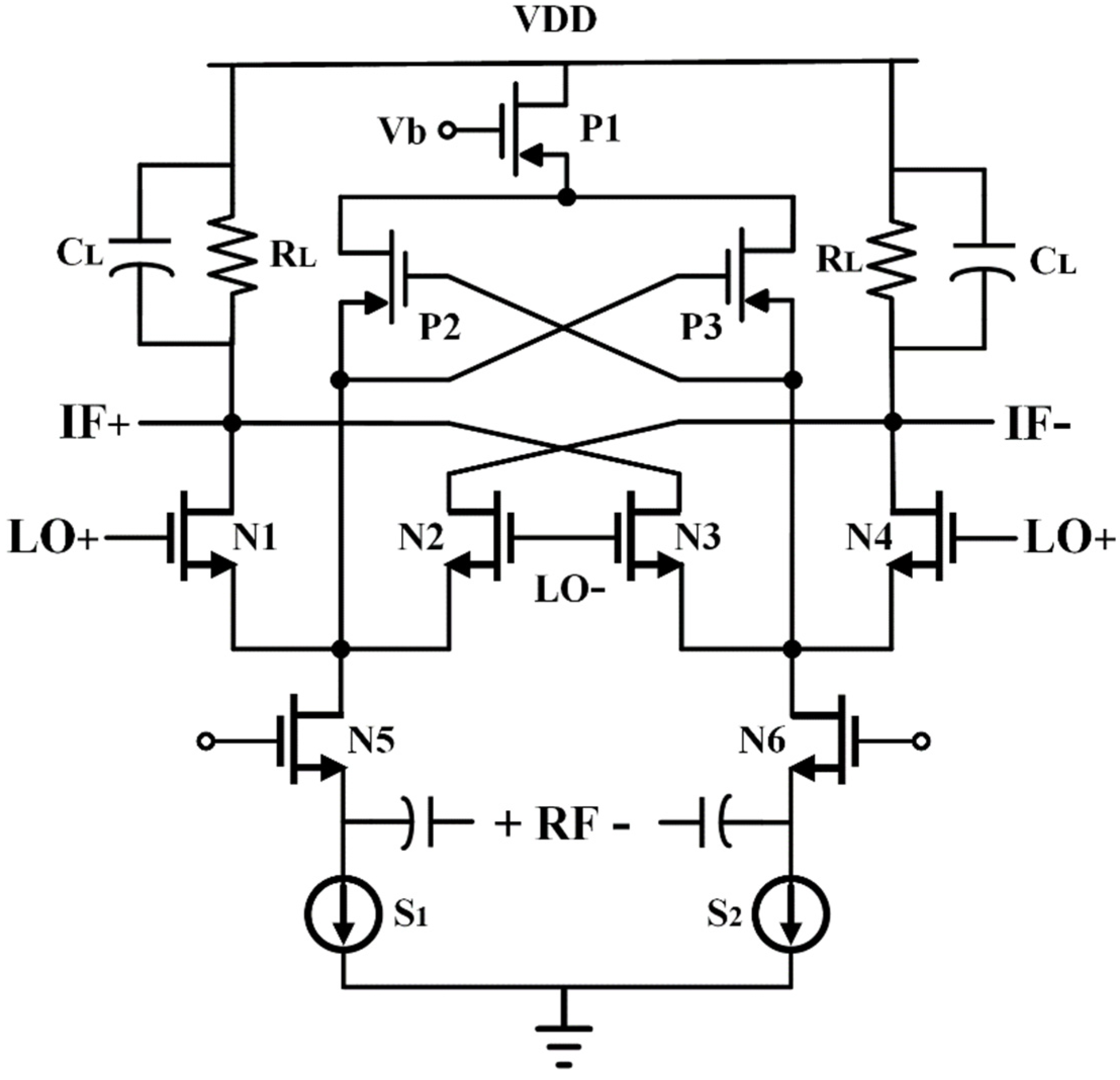
2. Circuit Design and Analysis

Figure 1 shows the schematic of the proposed mixer, which consists of four parts including the load stage (RL, CL), the switching stage (N1–N4), the negative impedance (P1–P3), and the transconductance stage (N5, N6) with current sources (S1, S2). The resistive load (RL) is in parallel with two small capacitors (CL) to eliminate the LO leakage and current spikes [16]. The negative impedance is actually a cross-coupled pair (P2, P3) with a current source (P1). The RF signal is input from the source of the transconductance stage. Through this source input method, a small input impedance can be obtained. The principle and analysis of the negative impedance technique and source input method will be described in detail below.

2.1. Negative Impedance

The noise of the mixer has a great influence on the sensitivity of the receiver. The flicker noise generated by the switching pairs has an important contribution to the overall noise of the mixer and it can be improved by reducing the bias current of the mixer switching pairs [17]. Conventionally, injecting a fixed current to the switches by the current sources, as shown in Figure 2a, reduces the effective current of them [18], which improves the flicker noise. However, this method increases the impedance seen at the source of the switches, resulting in more RF current to be shunted by the parasitic capacitance (CP) at that node. This reduces the mixer bandwidth and degrades its linearity. Since the flicker noise is mainly generated at the switching moment of the LO differential pairs [13], injecting a dynamic current at only the switching moment, which can avoid the problems caused by fixed injection, is a better way.
As shown in Figure 2b, the dynamic injection can be implemented by the negative impedance consisting of a cross-coupled pair (P2, P3) and a current source (P1). The nodes X and Y connect to the gates of P2 and P3, respectively. At the LO zero-crossings, the nodes voltage decreases, resulting in the cross-coupled pair turning on, injecting the current to the switching pairs. Otherwise, the nodes voltage is high, and the cross-coupled pair turns off, with no current injected.
In addition, the parasitic capacitance at the source of the switches will result in the flicker noise indirect translation to the output [17]. Fortunately, the negative impedance can neutralize part of the parasitic capacitance at that node, which improves the flicker noise further.
Under partial flicker noise cancelling condition, the negative impedance can increase the conversion gain by increasing the mixer output impedance for the transconductance stage. A detailed analysis is listed in Section 3.

2.2. Source Input

Conventionally, the RF signal is input from the gate of the transconductance stage in the Gilbert-cell mixer. However, the large impedance seen at the gate of the MOS transistor results in complicated impedance matching networks for broadband application. Figure 3a shows the LC ladder matching network that is commonly used in broadband mixers. In this network, a resistor (RM) is paralleled for good impedance matching, but it allows much noise and loss to be introduced. Moreover, the inductors (L1, L2) occupy a large chip area, especially in the frequency band below 10 GHz.
A better solution is to input the signal from the source of the transconductance stage, as shown in Figure 3b. The impedance seen at the signal input is approximately equal to 1 /   g m . Therefore, by adjusting the aspect ratio (W/L), the overdrive voltage (Vgs-Vth), and the flowing current of the transconductance transistor (N5), an impedance close to 50 Ω can be obtained, so that the input matching networks can be cancelled, and the problems caused by matching resistors and inductors can be avoided. The transconductance stage is biased by a current source to establish proper working conditions. The cascode topology is selected for the current source to suppress the channel length modulation effect. But the source input method will bring a challenge for the extreme low-power design that the current through the transistor cannot be too small to obtain a suitable g m for impedance matching.

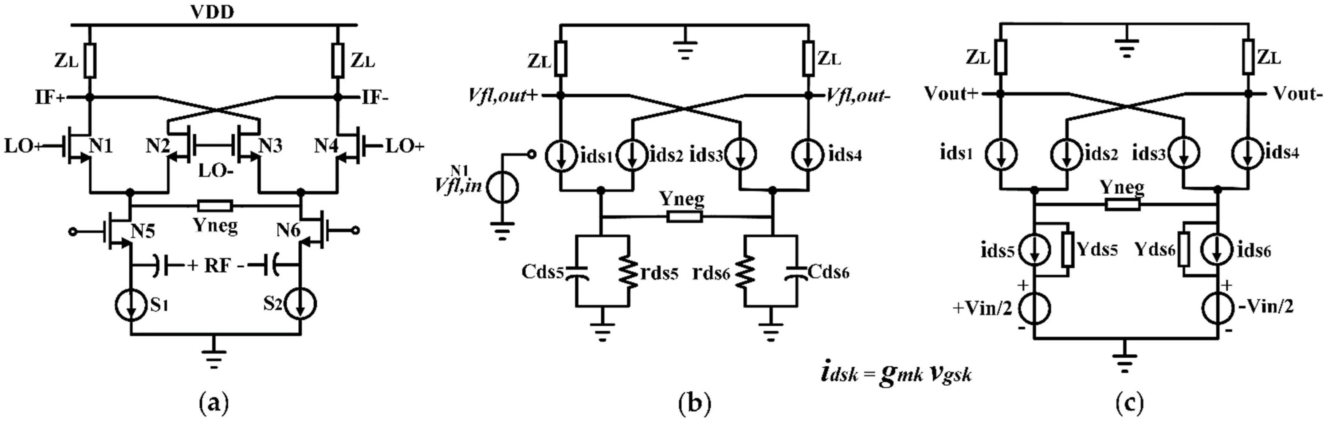
3. Derivation of the Mixer Parameters

As explained in Section 2, the techniques used in the proposed mixer improves the flicker noise and conversion gain of Gilbert-cell mixer. To further analyse the principle, the mathematical derivations of the mixer flicker noise and conversion gain are described in this Section.
The schematic in Figure 1 can be simplified as shown in Figure 4a (   Y n e g = G n e g + j ω C n e g   and   Z L = R L j 1 ω C L ). A few assumptions are made and given here according to [15,19].
(1)
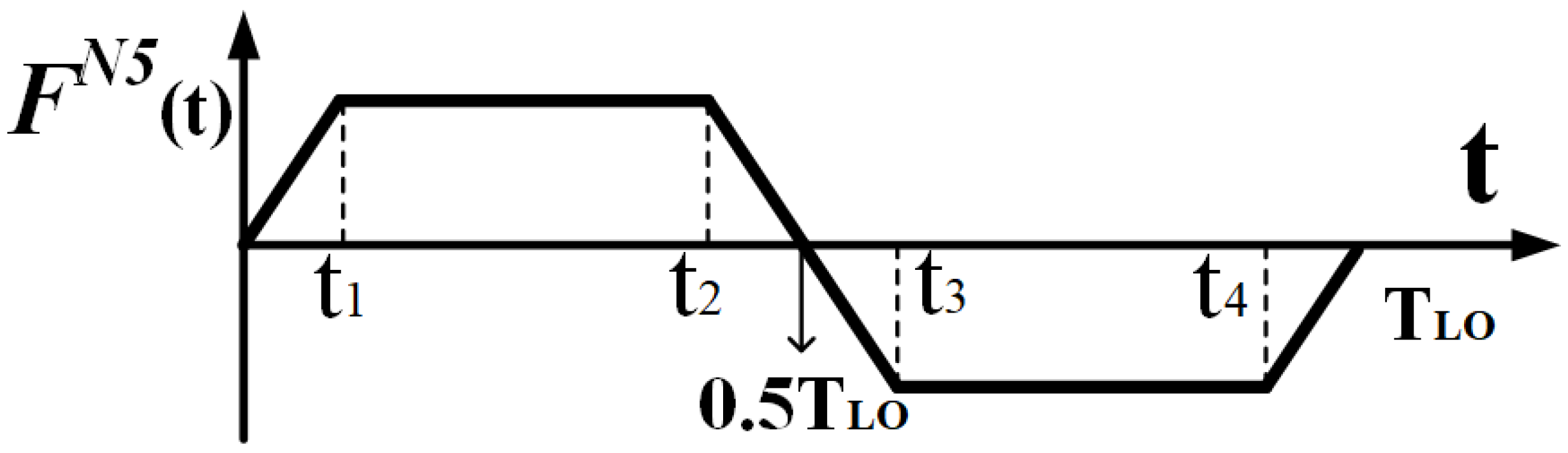
Assuming a symmetrical LO signal as shown in Figure 5, with the rise/fall time equal to α T LO , the constants t 1 and t 2 can be rewritten as t 1 = 0.5 α T LO , t 2   = 0.5 ( 1 α ) T LO .
(2)
In ( t 1 , t 2 ), N1 and N4 are on and N2 and N3 are off, while in ( t 3 , t 4 ), N1 and N4 are off and N2 and N3 are on.
(3)
S1 and S2 are ideal current sources with infinite internal impedance.

3.1. Flicker Noise

The time-varying small-signal model shown in Figure 4b can be used to analyse the flicker noise contributed by N1 in a LO period. The transconductance of N1–N6 and the output admittance of N5, N6 (   Y d s 5 , 6 = g d s 5 , 6 + j ω   C d s 5 , 6 ) are taken in account. V f l , i n N 1 is the source of flicker noise input from N1.
At ( t 1 , t 2 ), N1 and N5 can be regard as a common-source amplifier with a source negative feedback. The V f l , o u t N 1   | t 1 is given by:
                        V f l , o u t N 1   | t 1 = g m N 1 ( Y d s 5 + 2   Y n e g )   Z L g m N 1 + Y d s 5 + 2   Y n e g V f l , i n N 1
At ( t 2 , t 3 ), N1 and N5 are on, while at T LO / 2 , N1 and N5 form a balanced differential pair, and the output admittance is negligibly. The V f l , o u t N 1   | T LO / 2 is given by:
  V f l , o u t N 1   | T LO / 2 = g m N 1   Z L   V f l , i n N 1
At ( t 3 , t 4 ), N1 is off and there is no output.
        V f l , o u t N 1   | t 3 = 0  
Equation (1) shows that for   C n e g 0.5 C d s 5 and   G n e g ∈( ( g m N 1 g d s 5 ) / 2 , g d s 5 / 2 ), the real part of V f l , o u t N 1   | t 1 changes from negative to positive. In this condition, the approximated waveform of V f l , o u t N 1 in a LO period is given in Figure 6a,b. The negative impedance   Y n e g reduces the area of V f l , o u t N 1 in a LO period by changing the real part of V f l , o u t N 1 from negative to positive. This reduces the flicker noise leakage from the switches (N1–N4).

3.2. Convertion Gain

The time-varying small-signal model shown in Figure 4c can be used to derive the conversion gain. The first-order Fourier coefficient of the instantaneous voltage gain F ( t ) N 5 is given in Figure 7 in a LO period.
At ( t 1 , t 2 ), N2 and N3 are off, and N1, N4, N5 and N6 form a differential cacode common-gate amplifier. The F ( t ) N 5   | t 1 is given by:
F ( t ) N 5   | t 1 = g m N 1 ( g m N 5 + Y d s 5 )   Z L g m N 1 + Y d s 5 + 2   Y n e g
At ( t 3 , t 4 ), N1 and N4 are off, and N2, N3, N5 and N6 form a differential cacode common-gate amplifier. The F ( t ) N 5   | t 3 is given by:
F ( t ) N 5   | t 3 = F ( t ) N 5   | t 1  
At T LO / 2 and T LO , N1–N4 are on. There is no output due to the cancellation of differential symmetric.
F ( t ) N 5   | T LO / 2 = 0
According to [15,19], under the assumption of negligibly small transient effects, the conversion gain is derived by:
V G a i n = 2 s i n ( α π ) π 2 α   F ( t ) N 5   | t 1 = 2 s i n ( α π ) π 2 α   g m N 1 ( g m N 5 +   Y d s 5 )   Z L g m N 1 +   Y d s 5 + 2   Y n e g  
As Equation (7) shows, the conversion gain is increased by the negative impedance under partial flicker noise cancelling condition (   C n e g 0.5 C d s 3   and   G n e g ∈( ( g m N 1 g d s 5 ) / 2 , g d s 5 / 2 ). The reason for the increase is that the Y n e g increases the mixer output impedance for the transconductance stage.

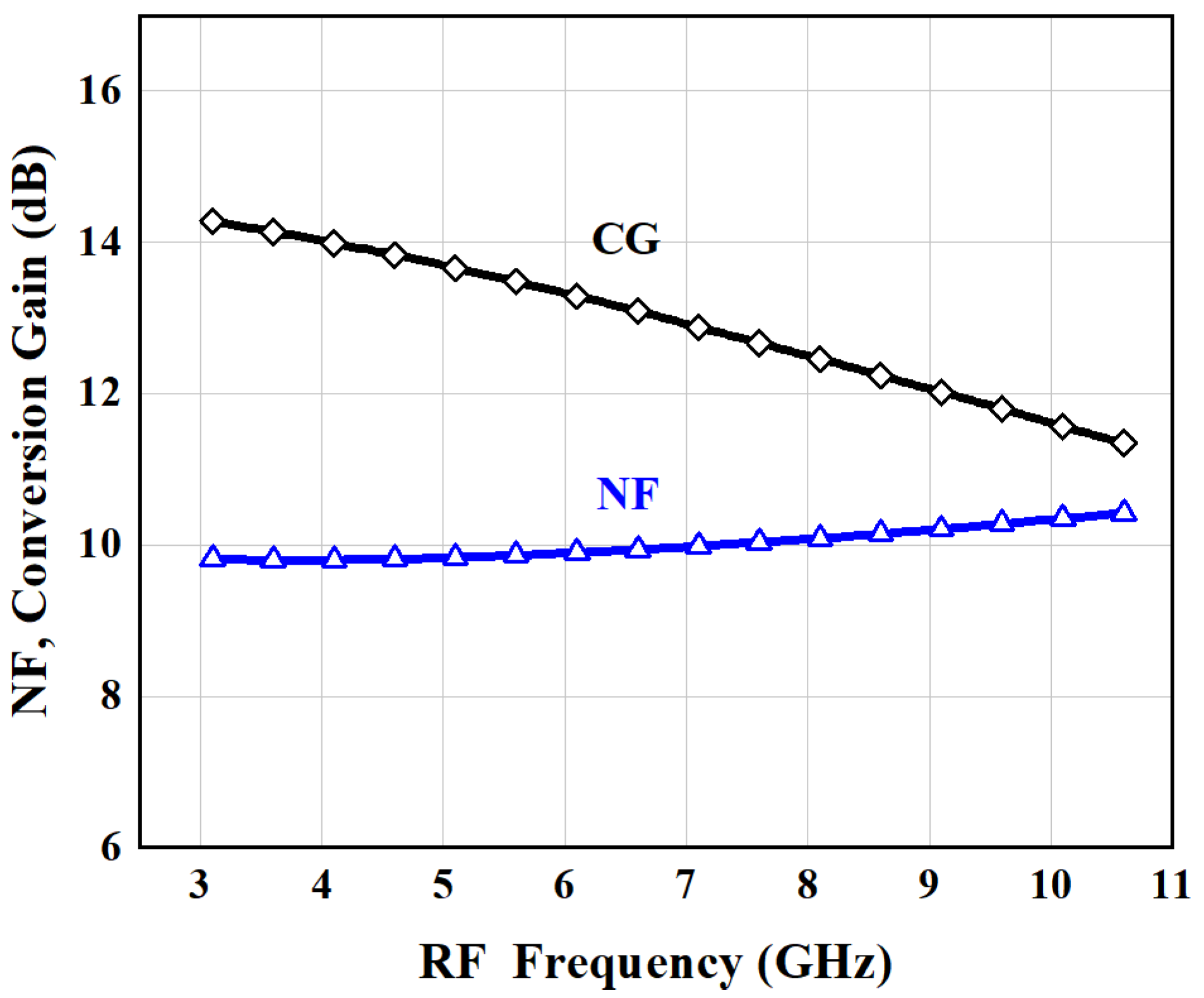
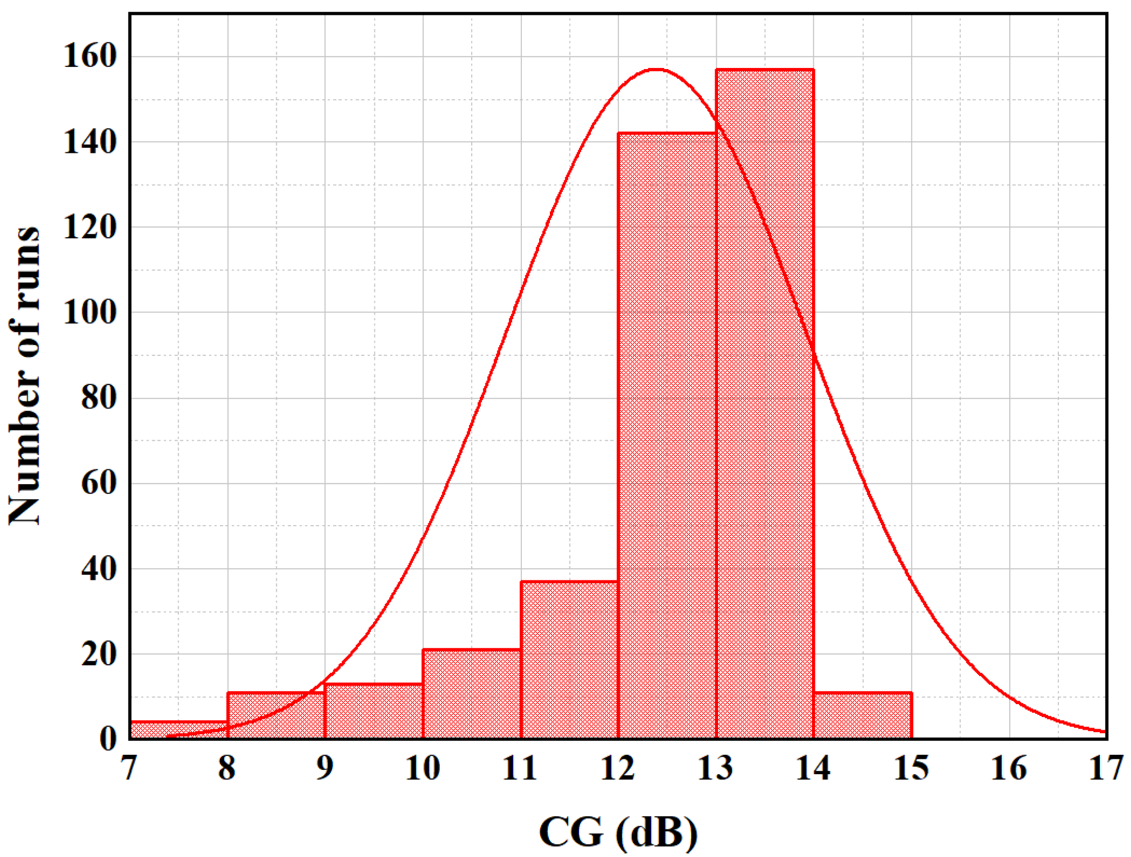
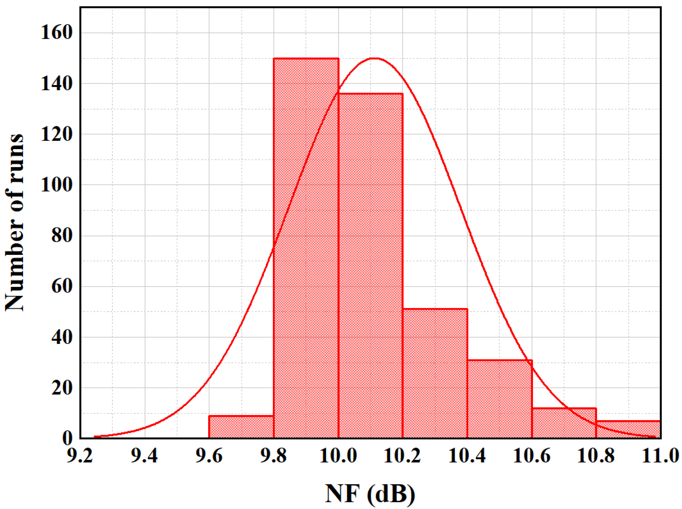
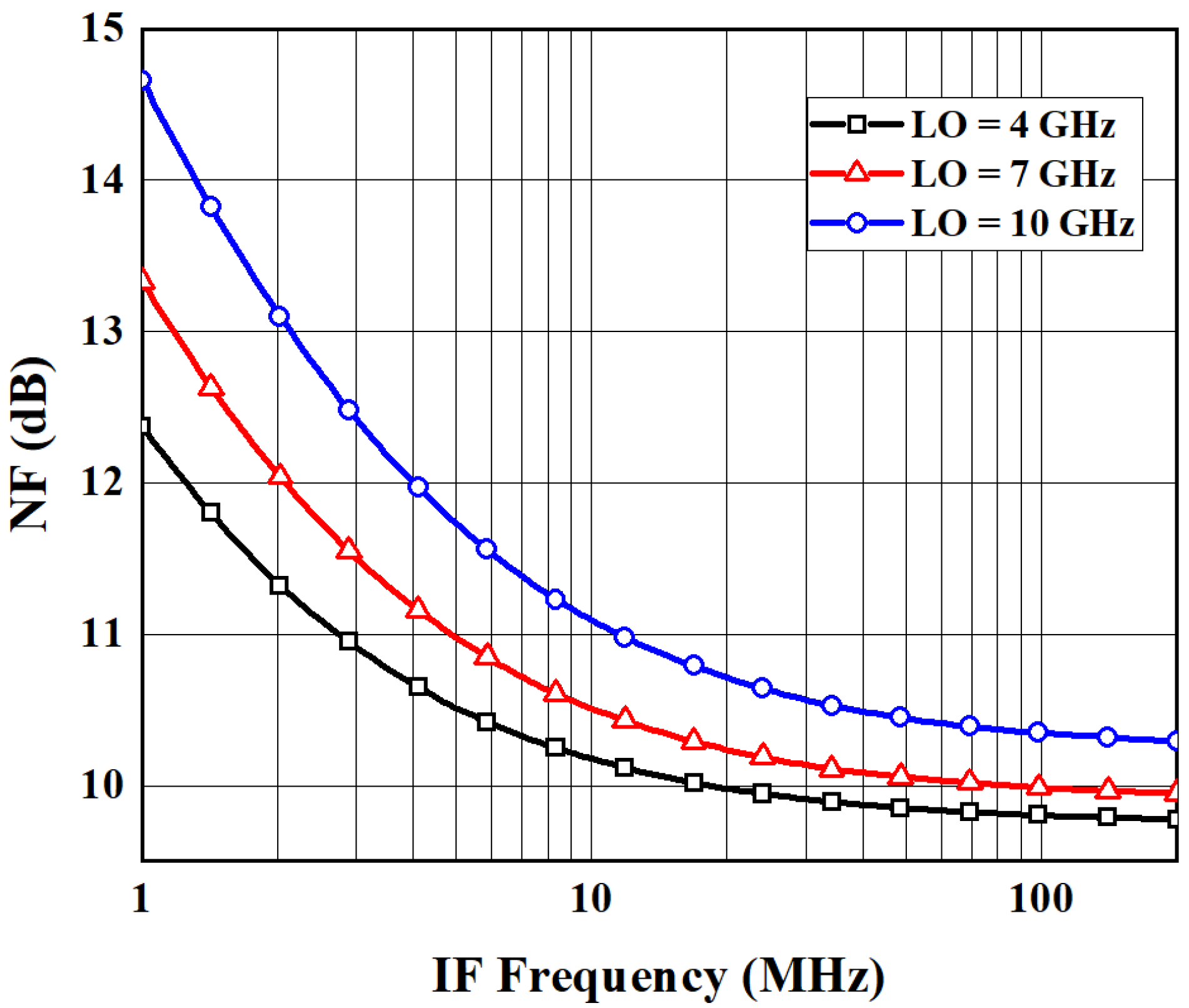
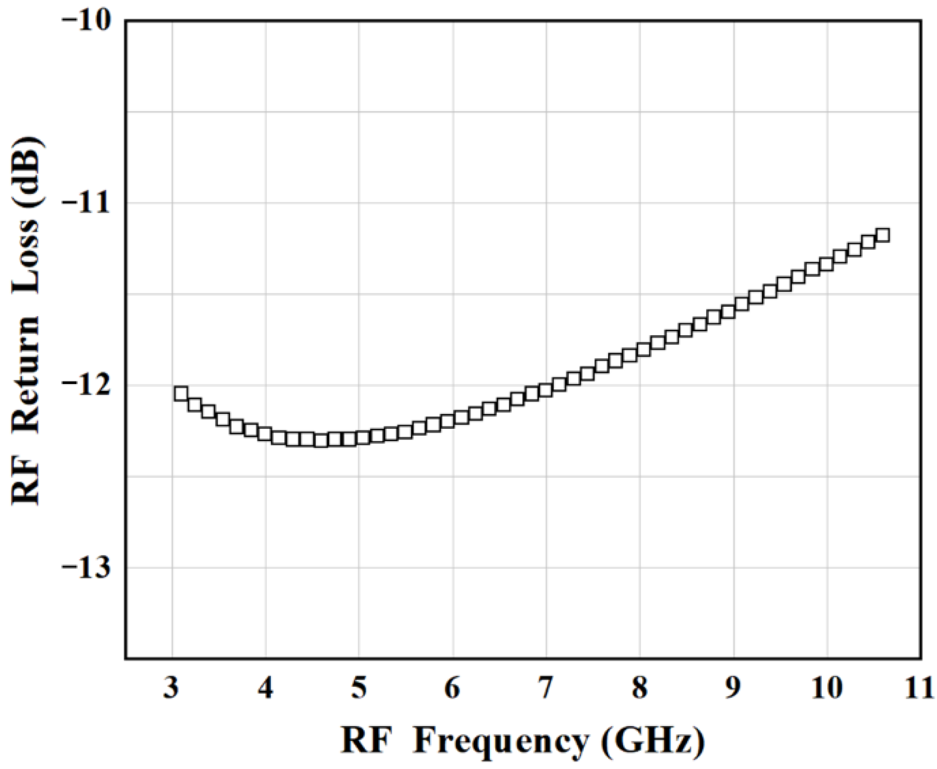
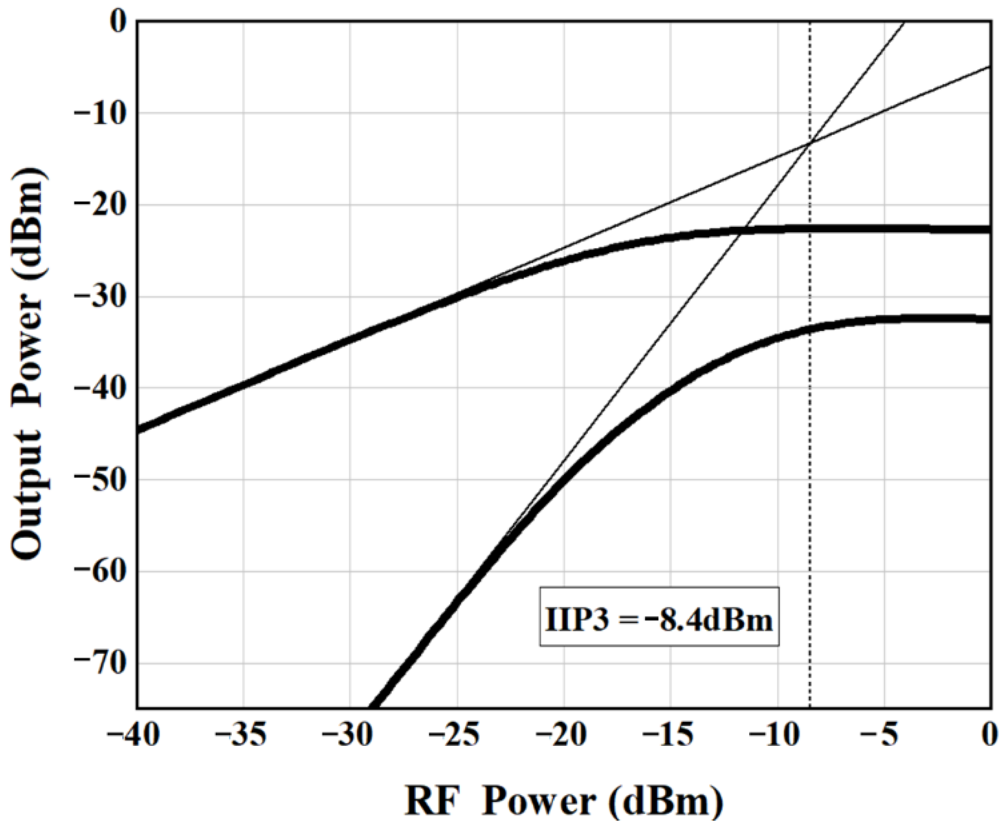
4. Simulation Results and Discussion

The presented mixer was designed in 45-nm SOI process provided by GlobalFoundries. Cadence Virtuoso was used to simulate the circuit. The matching impedance for both the RF and LO differential ports was 100 Ω. The RF input frequency was from 0.9 to 10.6 GHz, and the LO input frequency was set from 0.8 to 10.5 GHz. The intermediate frequency (IF) output frequency was 100 MHz. The LO input power used for the simulation was −1 dBm. The DC power consumption of the mixer core was 2.85 mW with the 1 V supply voltage.
Figure 8 shows the conversion gain (CG) and double-sideband (DSB) noise figure (NF) with the RF frequency sweeping from 3.1 to 10.6 GHz at an IF of 100 MHz. The maximum CG is 14.3 dB at 3.1 GHz and it reduces to 11.4 dB at 10.6 GHz. The minimum NF is 9.8 dB at 3.1 GHz and it increases to 10.6 dB at 10.6 GHz. Figure 9 and Figure 10 show the Monte-Carlo simulation results of the CG and NF, respectively, when the LO frequency is 6.5 GHz. For CG, around eighty-five percent of the runs are in the range of 11–14 dB, and for NF, about ninety percent of the runs are in the range of 9.8–10.6 dB. Therefore, the randomness of the process will not have a great impact on the CG and NF of the proposed mixer.
Figure 11 shows the NF plotted at various IF when the LO frequency is 4, 7 and 10 GHz. The NF increases with the decrease of IF, which is caused by the increase in flicker noise. Figure 12 shows the CG plotted at various LO power when the LO frequency is 4, 7 and 10 GHz. When the LO power is less than −2 dBm, the CG increases almost linearly with the increase of LO power. After that, the increase trend of the CG slows down, and the difference of the CG under different LO frequencies become larger. Thus, the increase of LO power will increase the CG, but the excessive LO power will reduce the flatness of CG in the broadband. Figure 13 shows that the RF port return loss is less than −11 dB, which indicates a good input impedance matching for the expected band.
Figure 14 shows a third-order input intercept point (IIP3) of −8.4 dBm when the LO frequency is 6.5 GHz. IIP3 is an indicator used to measure the linearity which is dependent on the overdrive voltage of the RF input transistors. The stacking of multiple transistors limits the ability of this circuit to provide high linearity in a lower supply voltage. Figure 15 shows the port-to-port isolations. The isolations of LO-to-RF and RF-to-IF are better than −48 dB, and the LO-to-IF isolation is better than −62 dB. Figure 16 shows the layout of the mixer that occupies an area of 0.39 × 0.69 mm2. Its core chip area excluding the pads is 0.16 × 0.16 mm2.
Table 1 summarizes the results and compares them with other advanced mixers. The mixer in [20] has a good NF of 8 dB, but it consumes a large DC power of 8.5 mW. The mixers in [21,22] have a large maximum CG more than 17 dB, but their CG is not flat enough, which changes more than 8 dB in the expected band. The conversion gain of the mixers in [7,8] has good flatness, but its maximum value does not exceed 10 dB. The mixers in [23,24] have an excellent IIP3 more than 8 dBm, but their NF is not satisfactory. Compared with other mixers, the proposed mixer has a high and flat CG of 11.4–14.3 dB, at a wide band of 7.5 GHz, and a low noise figure of 9.8 dB, while it occupied a small area of 0.39 × 0.69 mm2.

5. Conclusions

In this paper, a novel mixer with the negative impedance technique and source input method is proposed for UWB applications. The simulation results show that the proposed mixer obtains a wide band from 3.1 to 10.6 GHz with a conversion gain of 11.4–14.3 dB, a minimum noise figure of 9.8 dB, a RF port return loss of less than −11dB, a port-to-port isolation of better than −48 dB, and a core chip area of 0.16 × 0.16 mm2. Owing to the source input method, the proposed mixer achieves a good input impedance matching without matching networks. Combining the advantages of the negative impedance technique and source input method, the mixer shows a high and flat conversion gain, in a wide frequency band, a low noise figure, and a small chip size. Therefore, the proposed mixer meets the requirements of UWB systems perfectly, which makes the mixer very suitable for the applications of UWB systems.

Author Contributions

Conceptualization, investigation, and writing—original draft, Z.Z.; methodology, writing—review and editing, and supervision, X.L.; methodology, supervision, and funding acquisition, W.G. and X.W. All authors have read and agreed to the published version of the manuscript.

Funding

This research was funded by National Natural Science Foundation of China, grant number 61801027; China Postdoctoral Science Foundation, grant number 2018M631356; 111 Project of China, grant number B14010; Beijing Nova Program of Science and Technology, grant number Z191100001119078.

Conflicts of Interest

The authors declare no conflict of interest.

References

  1. Revision of Part 15 of the Commission’s Rules Regarding Ultra-Wideband Transmission Systems; FCC: Washington, DC, USA, 2002.
  2. Martín, J.S.; Cortés, A.; Zamora-Cadenas, L.; Svensson, B.J. Precise positioning of autonomous vehicles combining UWB ranging estimations with on-board sensors. Electronics 2020, 9, 1238. [Google Scholar] [CrossRef]
  3. Bao, D.; Zou, Z.; Nejad, M.B.; Qin, Y.; Zheng, L.-R. A wirelessly powered UWB RFID sensor tag with time-domain analog-to-information interface. IEEE J. Solid State Circuits 2018, 53, 2227–2239. [Google Scholar] [CrossRef]
  4. Vogli, E.; Ribezzo, G.; Grieco, L.A.; Boggia, G. Fast network joining algorithms in industrial IEEE 802.15.4 deployments. Ad Hoc Netw. 2018, 69, 65–67. [Google Scholar] [CrossRef]
  5. Liang, K.-H.; Chang, H.-Y.; Chan, Y.-J. A 0.5–7.5 GHz ultra low-voltage low-power mixer using bulk-injection method by 0.18-μm CMOS technology. IEEE Microw. Wirel. Compon. Lett. 2007, 17, 531–533. [Google Scholar] [CrossRef]
  6. Kuo, C.-L.; Huang, B.-J.; Kuo, C.-C.; Lin, K.-Y.; Wang, H. A 10–35 GHz low power bulk-driven mixer using 0.13-μm CMOS process. IEEE Microw. Wirel. Compon. Lett. 2008, 18, 455–457. [Google Scholar]
  7. Kim, M.G.; An, H.W.; Kang, Y.M.; Lee, J.Y.; Yun, T.Y. A low-voltage, low-power, and low-noise UWB mixer using bulk-injection and switched biasing techniques. IEEE Trans. Microw. Theory Tech. 2012, 60, 2486–2493. [Google Scholar] [CrossRef]
  8. Bhatt, D.; Mukherjee, J.; Redouté, J.-M. Low-power linear bulk-injection mixer for wide-band applications. IEEE Microw. Wirel. Compon. Lett. 2016, 26, 828–830. [Google Scholar] [CrossRef]
  9. Klumperink, E.A.M.; Louwsma, S.M.; Wienk, G.J.M.; Nauta, B. A CMOS Switched Transconductor Mixer. IEEE J. Solid State Circuits 2004, 39, 1231–1240. [Google Scholar] [CrossRef] [Green Version]
  10. Lee, S.; Bergervoet, J.; Harish, K.S.; Leenaerts, D.; Roovers, R.; van de Beek, R.; van der Weide, G. A Broadband Receive Chain in 65nm CMOS. In Proceedings of the IEEE International Solid-State Circuits Conference, San Francisco, CA, USA, 11–15 February 2007; pp. 418–420. [Google Scholar]
  11. Li, H.; El-Gabaly, A.M.; Saavedra, C.E. A low-power low-noise decade-bandwidth switched transconductor mixer with AC-coupled LO buffers. IEEE Trans. Circuits Syst. 2018, 65, 510–521. [Google Scholar] [CrossRef]
  12. NacEachern, L.A.; Manku, T. A charge-injection method for Gilbert cell biasing. In Proceedings of the IEEE Canadian Conference on Electrical and Computer Engineering, Waterloo, ON, Canada, 25–28 May 1998; pp. 365–368. [Google Scholar]
  13. Darabi, H.; Chiu, J.A. Noise cancellation technique in active RF-CMOS mixers. IEEE J. Solid-State Circuits 2005, 40, 2628–2632. [Google Scholar] [CrossRef]
  14. Yoon, J.; Kim, H.; Park, C.; Yang, J.; Song, H.; Lee, S.; Kim, B. A new RF CMOS Gilbert mixer with improved noise figure and linearity. IEEE Trans. Microw. Theory Tech. 2008, 56, 626–631. [Google Scholar] [CrossRef]
  15. Cheng, W.; Annema, A.J.; Wienk, G.J.M.; Nauta, B. A flicker noise/IM3 cancellation technique for active mixer using negative impedance. IEEE J. Solid State Circuits 2013, 48, 2390–2402. [Google Scholar] [CrossRef] [Green Version]
  16. Motieifar, A.; Pour, Z.A.; Bridges, G.; Shafai, C.; Shafai, L. An ultra wideband (UWB) mixer with 0.18um RF CMOS technology. In Proceedings of the IEEE Canadian Conference on Electrical and Computer Engineering, Ottawa, ON, Canada, 7–10 May 2006; pp. 697–700. [Google Scholar]
  17. Darabi, H.; Abidi, A.A. Noise in RF-CMOS mixers: A simple physical model. IEEE J. Solid State Circuits 2000, 35, 15–25. [Google Scholar] [CrossRef]
  18. Sansen, W.M.C.; Meyer, R.G. Distortion in bipolar transistor variable-gain amplifiers. IEEE J. Solid State Circuits 1973, 8, 275–282. [Google Scholar] [CrossRef]
  19. Cheng, W.; Annema, A.J.; Croon, J.A.; Nauta, B. Noise and nonlinearity modeling of active mixers for fast and accurate estimation. IEEE Trans. Circuits Syst. 2011, 2, 276–289. [Google Scholar] [CrossRef]
  20. Jouri, M.; Golmakani, A.; Yahyabadi, M.; Khosrowjerdi, H. Design and simulation of a down-conversion CMOS mixer for UWB applications. In Proceedings of the International Conference on Electrical Engineering/Electronics, Computer, Telecommunications and Information Technology, Chiang Mai, Thailand, 19–21 May 2010; pp. 937–940. [Google Scholar]
  21. Zhang, X.; Cui, X.; Wang, B.; Lee, C.L. A high gain, wide band (2–10 GHz), and low noise active balun merged folded mixer for the full-band UWB application. In Proceedings of the IEEE International Wireless Symposium, Beijing, China, 14–18 April 2013; pp. 1–3. [Google Scholar]
  22. Chen, J.-D.; Qian, J.-B.; Huang, S.-Y. Low-noise and high-gain folded mixer for a UWB System in 0.18-μm SiGe Bi-CMOS technology. IEEE Trans. Circuits Syst. 2021, 68, 612–616. [Google Scholar]
  23. Ebrahimi, A.; Hemmati, M.J.; Hakimi, A.; Afrooz, K. A new low-power and high-linearity CMOS bulk injection mixer in 0.13 μm technology. In Proceedings of the Iranian Conference on Electrical Engineering, Mashhad, Iran, 8–10 May 2018; pp. 108–113. [Google Scholar]
  24. Seyedi, H.; Dehdasht-Heydari, R.; Roshani, S. UWB down-conversion mixer using an IM3 cancellation modified technique for zero and low IF applications. Microelectron. J. 2021, 109, 104983–104989. [Google Scholar] [CrossRef]
Figure 1. The proposed mixer schematic.
Electronics 10 02655 g001
Figure 2. (a) The conventional fixed-injection method of Gilbert mixer; (b) The dynamic-injection method of Gilbert mixer and corresponding waveform.
Electronics 10 02655 g002
Figure 3. (a) The LC ladder matching network; (b) The source input method that allows the input matching networks to be cancelled.
Electronics 10 02655 g003
Figure 4. (a) Simplified schematic of the proposed mixer; (b,c) Time-varying small-signal model to analyse the flicker noise and the conversion gain, respectively.
Electronics 10 02655 g004
Figure 5. The assumed LO waveform.
Electronics 10 02655 g005
Figure 6. (a,b) Approximated waveform of the real and imaginary parts of V f l , o u t N 1 , respectively.
Electronics 10 02655 g006
Figure 7. Approximated waveform of the instantaneous voltage gain F ( t ) N 5 .
Electronics 10 02655 g007
Figure 8. Noise figure (NF) and conversion gain (CG) versus to RF frequency at an IF of 100 MHz.
Electronics 10 02655 g008
Figure 9. Monte-Carlo simulation of CG when the LO frequency is 6.5 GHz.
Electronics 10 02655 g009
Figure 10. Monte-Carlo simulation of NF when the LO frequency is 6.5 GHz.
Electronics 10 02655 g010
Figure 11. Noise figure (NF) versus to IF frequency at the LO of 4, 7 and 10 GHz.
Electronics 10 02655 g011
Figure 12. Conversion gain (CG) versus to LO power at the LO of 4, 7 and 10 GHz.
Electronics 10 02655 g012
Figure 13. Return loss of RF port.
Electronics 10 02655 g013
Figure 14. Third-order input intercept point (IIP3) at the LO of 6.5 GHz.
Electronics 10 02655 g014
Figure 15. Isolations between the RF, LO, and IF ports.
Electronics 10 02655 g015
Figure 16. The mixer layout with an area of 0.39 × 0.69 mm2.
Electronics 10 02655 g016
Table 1. Performance summary and comparison.
Refer.Freq.
(GHz)
Process
(um)
IF
(MHz)
CG
(dB)
LO
(dBm)
DSB NF
(dB)
IIP3 (dBm)VDD
(V)
PDC
(mW)
Area
(mm)
10′ [20] a3–110.182509.5–12.5-821.88.5-
12′ [7] b0.2–130.182645.6–9.9511.7−100.80.880.58 × 0.62
13′ [21] a2–100.181008.1–17.6612.6−1.71.87.80.77 × 1.14
16′ [8] b1–60.181004–78.713.501.80.63-
21′ [22] b3–110.182648.8–17.179.8−52.50.630.88 × 0.89
18′ [23] a3.1–8.50.131012.7–13.7−613.78.51.60.45-
21′ [24] a0.9–50.065110.8–11.8516.920.51.23.50.13 × 0.39 *
This work a3.1–10.60.04510011.4–14.3−19.8−8.412.850.39 × 0.69
a simulation b measurement * excluding pads.
Publisher’s Note: MDPI stays neutral with regard to jurisdictional claims in published maps and institutional affiliations.

