Article

Improved Cascaded H-Bridge Multilevel Inverters with Voltage-Boosting Capability

1
Electrical and Electronic Engineering, Newcastle University in Singapore, 172A Ang Mo Kio Avenue 8 #05-01, Singapore 567739, Singapore
2
College of Electrical Engineering, Zhejiang University, Hangzhou 310027, China
3
Faculty of Engineering and Information Technology, University of Technology Sydney, Ultimo, NSW 2007, Australia
*
Author to whom correspondence should be addressed.
Electronics 2021, 10(22), 2801; https://doi.org/10.3390/electronics10222801
Submission received: 27 October 2021 / Revised: 10 November 2021 / Accepted: 15 November 2021 / Published: 15 November 2021

Abstract

:
This paper proposes two improved cascaded H-bridge (ICHB) multilevel inverters that feature voltage-boosting capability. The conventional H-bridge with a front-end dc–dc boost converter was restructured for single-stage operation. The developed three-level topology not only saves one power switch but also exhibits lower voltage stress across its capacitor. Extension to five-level generation was also introduced by merely adding two power switches and one capacitor. The final five-level topology outperforms the classical cascaded H-bridge (CHB) multilevel inverter with a significant reduction in the power switch count, with a 42% and 50% reduction in both the isolated dc source and inductor counts. The power efficiency was also improved without compromising the modularity feature of the classical CHB multilevel inverter. The operation and theoretical analysis of the proposed topologies were validated via simulations and experimental tests.

1. Introduction

The establishment of the first multilevel inverter dates to 1971. The cascaded H-bridge (CHB) [1] has revolutionized the dc-to-ac power conversion since its introduction. It has become a highly developed and mature technology for various industrial and renewable energy applications after a few decades of improvement [2,3,4,5,6,7]. Today, researchers are continuously improving the compactness and efficiency of cascaded multilevel inverters by establishing various topologies with reduced switch counts and fewer conversion stages [8].
One popular approach to lower the switch count is to adopt a hybrid concept that divides the voltage level generation and polarity inversion into two stages [9]. Multiple half-bridges that respectively control an isolated dc source are cascaded to generate multiple levels of a unipolar voltage across the dc-link of an H-bridge. The H-bridge is operated at the line frequency with a duty cycle of 0.5 to generate a multilevel ac voltage. This type of topology is referred to as a multilevel dc-link inverter, and its half-bridges can be replaced by different modules to favorably increase the number of levels with minimal switch count. For example, a switched-diode module in place of a half-bridge is able to reduce the essential power switches from six to three for controlling three isolated dc sources [10].
Compact modules that control multiple isolated dc sources for bipolar ac voltage generation without a rear-end H-bridge have also been explored in recent years. In Ref. [11], an E-type module that integrates a half-bridge and a T-type inverter with four additional switches was presented. It uses four isolated dc sources with asymmetrical magnitudes to generate 13 voltage levels. The E-type module can be extended to generate an ac voltage of 17 levels by adding two additional power switches [12]. An optimized module for the cascaded multilevel inverter in [13] achieves the least switches per level generation. However, the requirement of multiple isolated dc sources for each module leads to an uneven duration to supply the load, which, in turn, results in a power-balancing issue. Therefore, it does not preserve the modularity feature of the conventional CHB [14].
One common limitation of all the above modules is that their voltage gain is restricted to unity, which is similar to the classical CHB multilevel inverter. They require the same number and magnitude as isolated dc sources as those in the CHB. Considering a PV source that generates low dc voltage in each module, a large number of series-connected PV modules are necessary to achieve a sufficient magnitude of ac voltage. Alternatively, a boost dc–dc converter can be added between PV source and inverter module. This two-stage power conversion, however, uses more components and reduces power efficiency. In light of this, there is a growing trend in developing inverter topologies with integrated voltage-boosting. To achieve single-stage power conversion, the concept of a Z-source inverter was adopted in [15] by integrating a quasi-switched impedance network into each H-bridge. In [16], a five-level boost inverter module was established by using 10 power switches, 2 inductors, and 2 capacitors.
Two improved CHB topologies are proposed in this paper, i.e., a three-level configuration and a 5five-level configuration that provides voltage-boosting without sacrificing the modularity feature of the conventional CHB. Moreover, they also exhibit higher compactness with a reduced number of switches, isolated dc sources, and inductors. The rest of the paper is organized as follows. Section 2 presents the steady-state analysis of the proposed improved CHB topologies and their pulse-width modulation (PWM) technique. Section 3 benchmarks the proposed topologies with the existing cascaded multilevel inverters. The simulation and experimental results are discussed in Section 4. Finally, Section 5 concludes this paper.

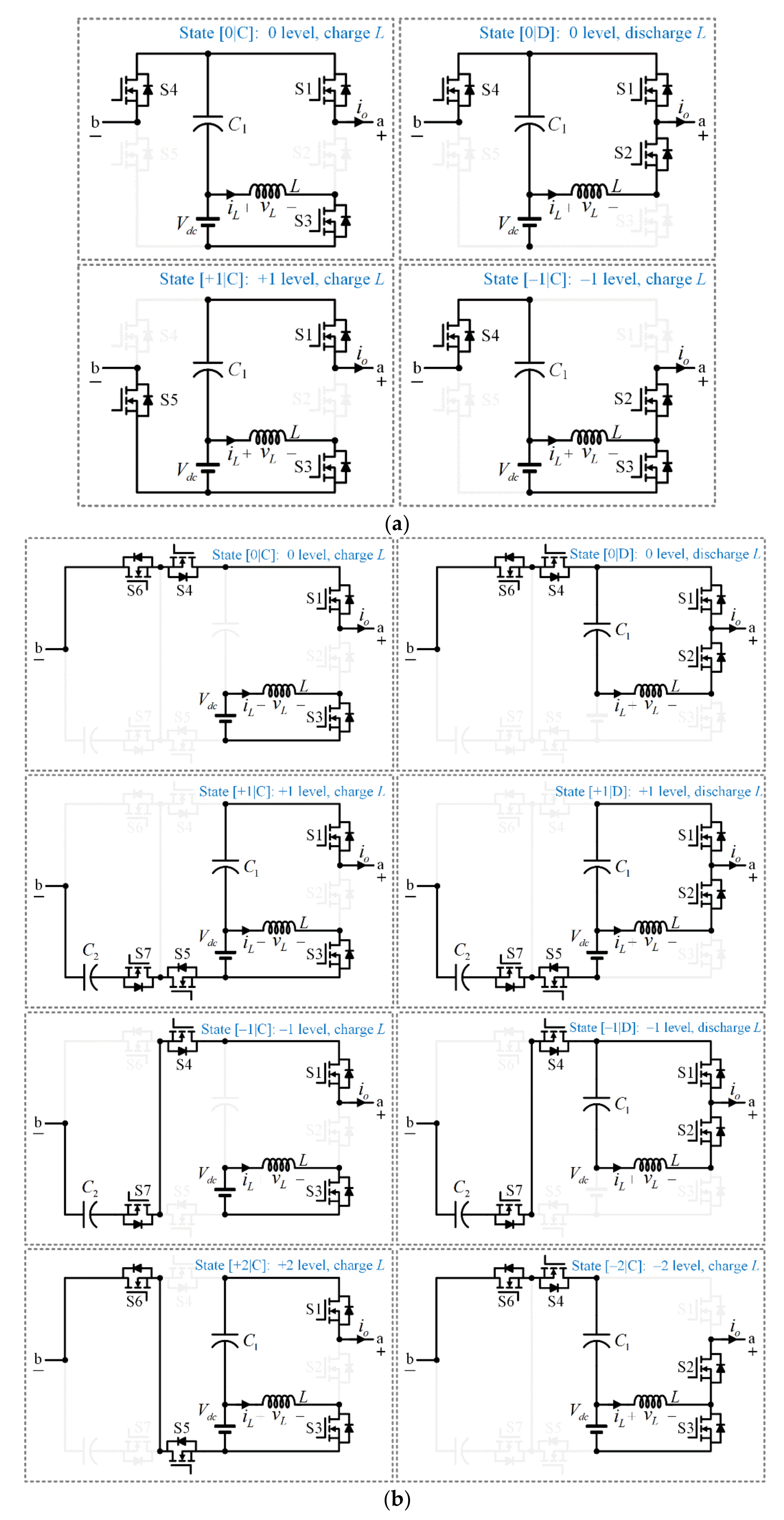
2. Proposed ICHB Multilevel Inverters
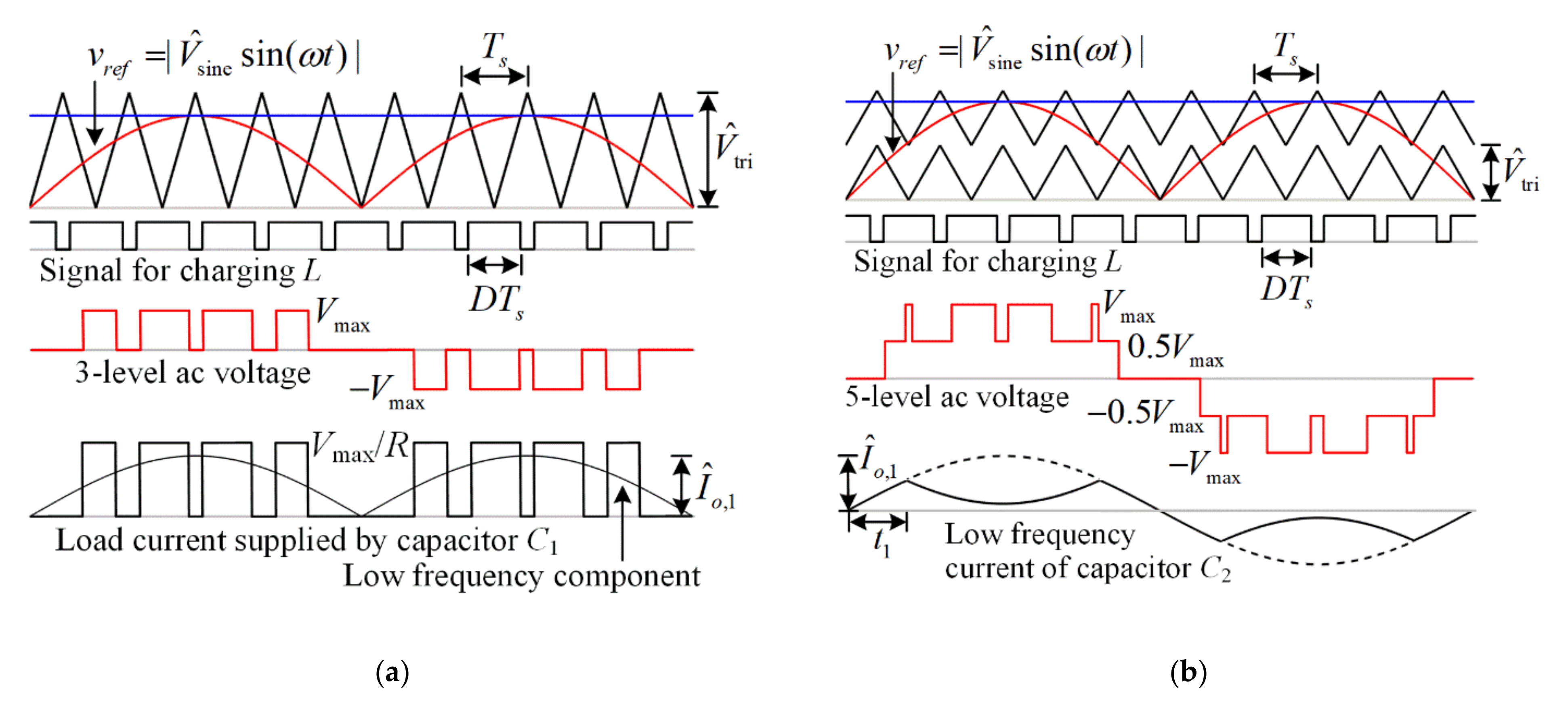
2.1. ICHB (3L)

The use of a front-end dc–dc boost converter in a classical CHB multilevel inverter is mandatory to boost the voltage. The resultant two-stage structure is depicted in Figure 1a. Some structural modifications of such a configuration enable a concurrent achievement of voltage-boosting and ac voltage generation within a single-stage operation. The established topology is referred to as ICHB (3L), and it uses one switch less than the CHB with a front-end boost converter, as illustrated in Figure 1b. The reorganized structure shows that the capacitor C1 is connected in series with the dc source, thus alleviating its voltage stress.
Referring to the switching states in Figure 2a, it is known that the proposed ICHB (3L) is able to generate three ac voltage levels, while simultaneously charging the boost inductor with a constant duty cycle D, according to the modulation scheme in Figure 3a. By taking the volt-second balance across the inductor L, the average voltage of the capacitor C1 is obtained as
V C 1 = D 1 D V d c
The maximum ac voltage level Vmax is the sum of the capacitor and dc source voltages. That is,
V max = 1 1 D V d c
By controlling the modulation index M, the amplitude of the fundamental ac voltage V ^ o , 1 can be written as
V ^ o , 1 = M 1 D V d c
The voltage ripple of the capacitor C1 and current ripple of the inductor L consist of low-frequency and high-frequency components due to the single-phase load and the pulse-width modulation (PWM), respectively. The low-frequency voltage ripple of C1 can be obtained by analyzing the double-line-frequency current flowing through this capacitor. Through Fourier analysis, the double-line-frequency component of the rectified load current depicted in Figure 3a is derived. Considering the impedance of C1 at double-line-frequency, the low-frequency voltage ripple Δ V C 1 , 2 f o of capacitor C1 can be written as
Δ V C 1 , 2 f o = 4 I ^ o , 1 6 π 2 f o C 1
where I ^ o , 1 is the amplitude of the load current at the line frequency f o . Considering the ideal dc source, the voltage across the inductor at double-line frequency can be calculated by multiplying the capacitor C1 voltage with (1-D). Considering the impedance of inductor L at double-line frequency, the low-frequency current ripple Δ I L , 2 f o of the inductor L is given by the following expression:
Δ I L , 2 f o = ( 1 D ) I ^ o , 1 6 π 3 f o 2 L C 1
As the inductor is charged with a constant duty cycle D, the high-frequency ripple of the capacitor voltage Δ V C 1 , f s and inductor current Δ I L , f s are similar to the equations of the boost dc–dc converter that can be respectively written as
Δ V C 1 , f s = 2 D I ^ o , 1 π f s C 1
Δ I L , f s = D V d c f s L

2.2. ICHB (5L)

The number of voltage levels can be further extended to five by integrating merely two additional power switches and one additional capacitor, as depicted in Figure 1c. The switching states in Figure 2b show that the capacitor C2 is operated symmetrically over each half-cycle, signifying that the capacitor voltage is balanced naturally at 0.5 Vmax. Figure 3b shows the extended PWM scheme for the proposed ICHB (5L). Based on the current waveform depicted in Figure 3b, the charge balance of C2 is clearly seen in each fundamental cycle. The amount of electric charge flowing into the capacitor in each fundamental cycle can be obtained by integrating the current in positive half-cycle. By dividing electric charge by the capacitance, the voltage ripple Δ V C 2 of C2 can be written as
Δ V C 2 = I ^ o , 1 π f o C 2 1 + π 2 M 2 cos sin 1 1 2 M 1 M sin 1 1 2 M

2.3. Cascaded Extension

Both the proposed ICHB (3L) and ICHB (5L) topologies preserve the modularity of the conventional CHB, and they can be conveniently extended by cascading n modules controlled by the same reference signals. The phase shift of the triangular carrier for the mth module is
θ t r i , m = 360 ° n m 1
where m = {1, 2, …, n}. The maximum number of voltage levels for n cascaded ICHB (3L) and ICHB (5L) is, respectively, expressed as
N l e v e l ICHB ( 3 L ) = 2 n + 1
N l e v e l ICHB ( 5 L ) = 4 n + 1

3. Comparison with CHB Multilevel Inverter

Table 1 compares the proposed topologies and the classical CHB. While the voltage gain of a classical CHB was restrained to unity, the comparison was made for the classical CHB with an integrated front-end boost converter, as shown in Figure 1a. Considering the same number of voltage levels, noteworthy advantages of the proposed topologies are listed as follows.
Superiority of the proposed ICHB (3L) over a conventional single CHB module (Figure 1a with n = 1):
(1)
Reduced switch count from 6 to 5.
(2)
Reduced capacitor voltage stress from Vmax to DVmax.
(3)
Reduced total standing voltage (TSV) of the inverter from 6Vmax to 5Vmax.
Superiority of the proposed ICHB (5L) over two cascaded conventional CHB modules (Figure 1a with n = 2):
(1)
Reduced switch count by 42%, i.e., from 12 to 7.
(2)
Reduced number of isolated dc sources from 2 to 1.
(3)
Reduced inductor count from 2 to 1.
It is worth emphasizing that the advantages of the proposed topologies are more apparent when more levels are generated. Take the nine-level generation as an example, in which the number of cascaded modules required for a classical CHB with a boost converter is four. On the contrary, the proposed ICHB (5L) requires only two cascaded modules to achieve the same number of levels. This implies that it saves 10 power switches, 2 isolated dc sources, and 2 inductors compared to the CHB with a front-end boost converter. In short, the voltage boost function and single-stage power conversion of both the proposed topologies greatly improve the compactness and efficiency of the classical CHB. The proposed topologies are also more compact than the latest boost inverter modules. For a three-level module, each ICHB (3L) saves two diodes compared with [15]. The proposed ICHB (5L) can generate the same number of voltage levels (five-level) as [16] while using significantly lesser components by saving three power switches, one inductor, and one capacitor.

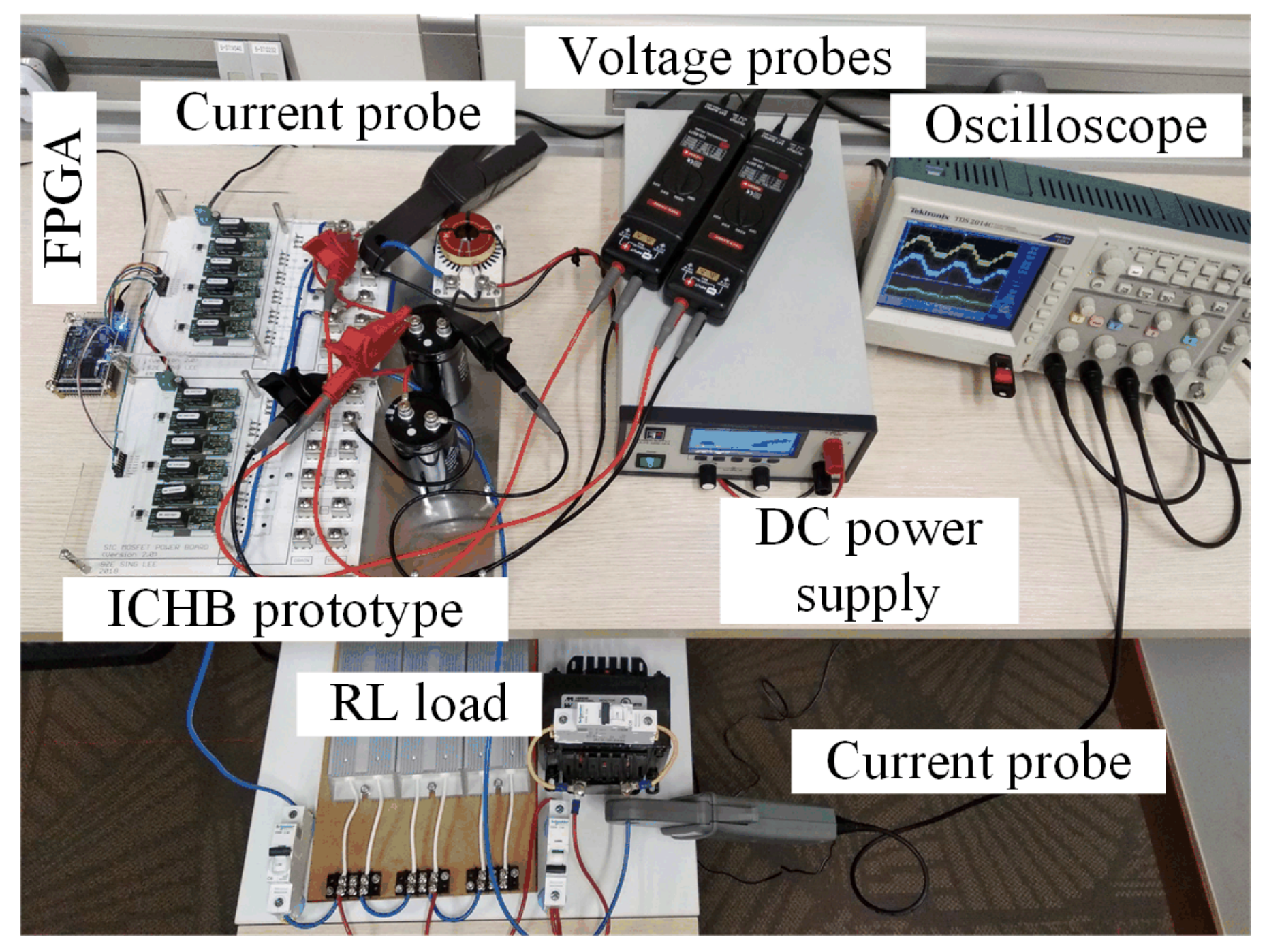
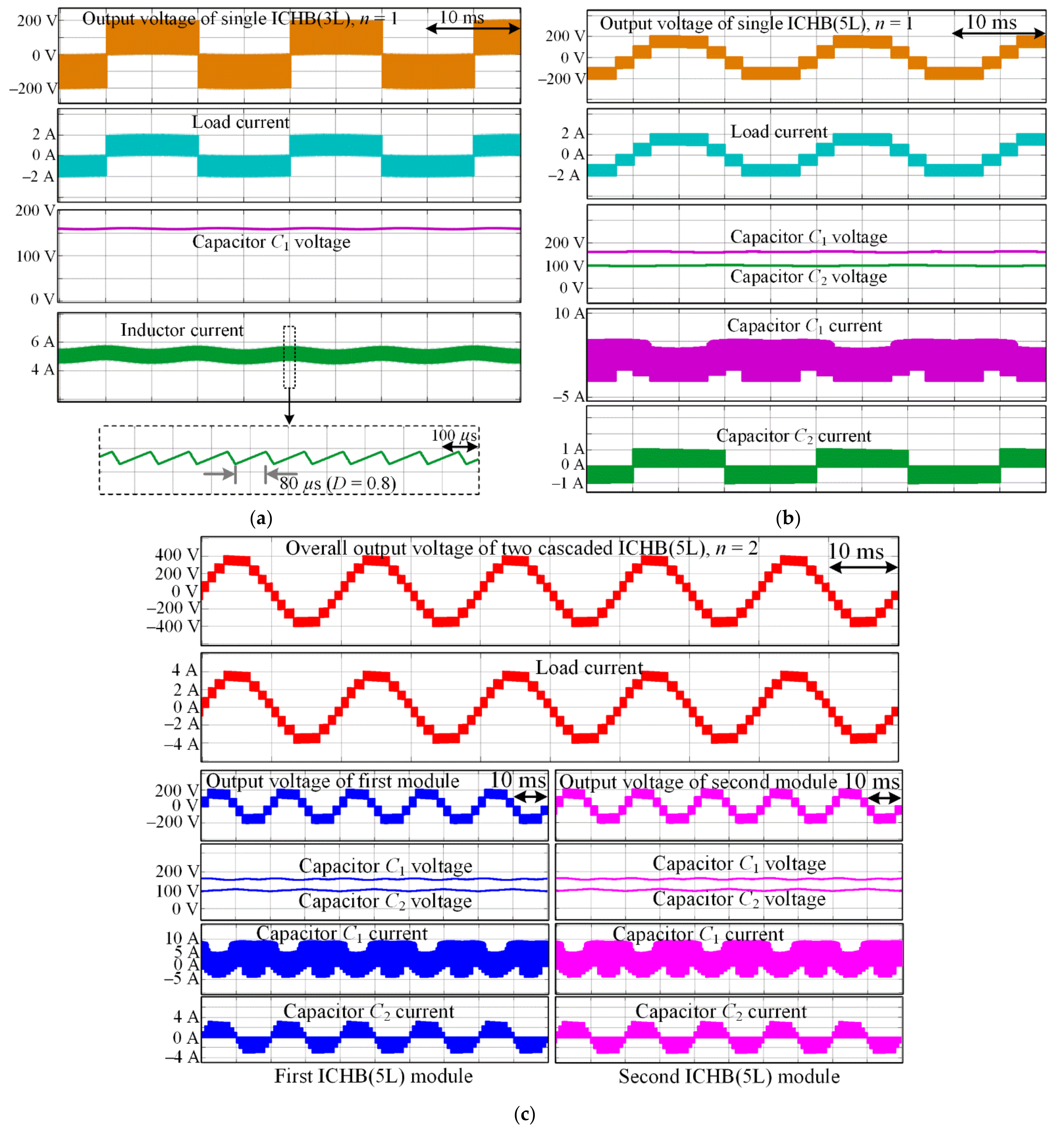
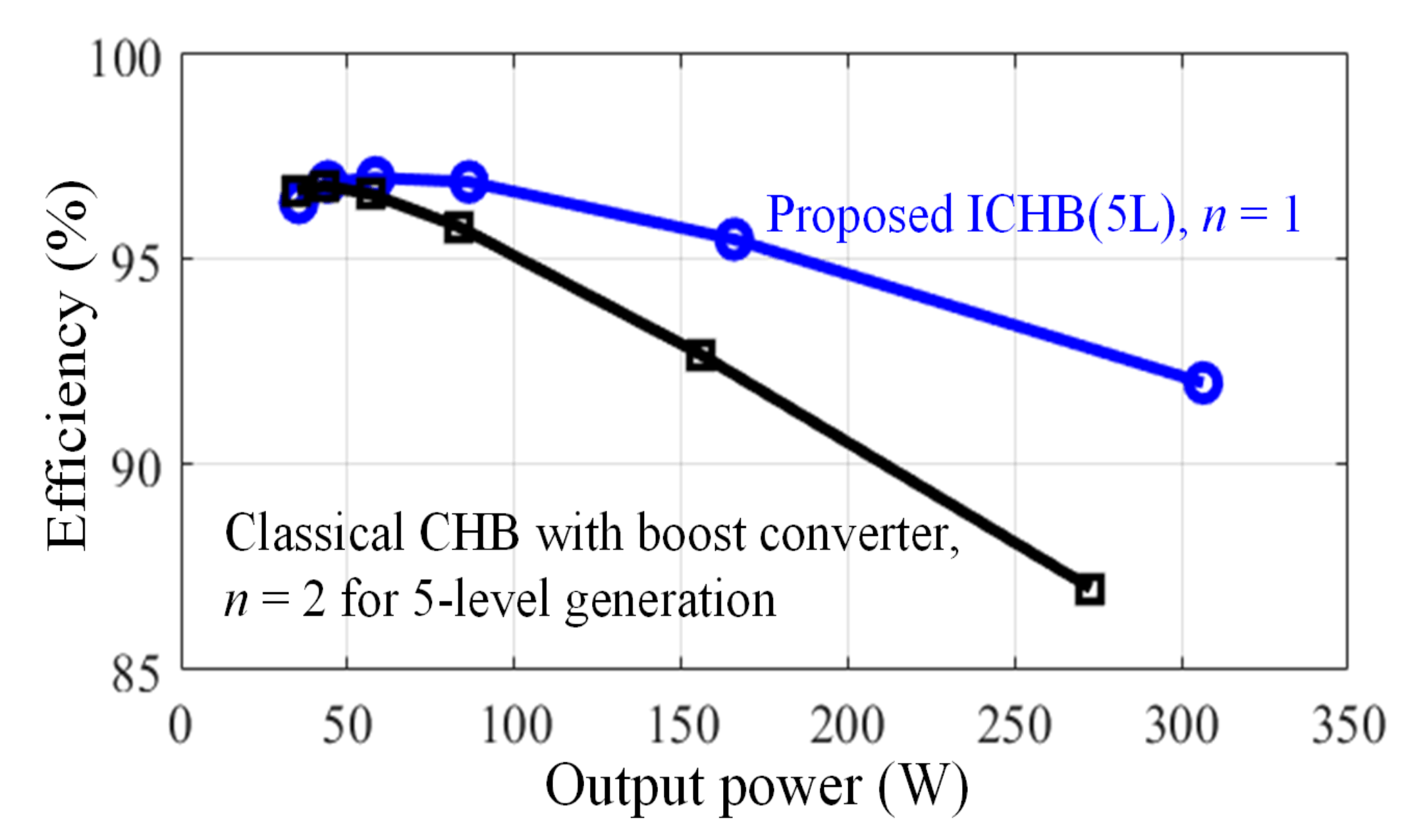
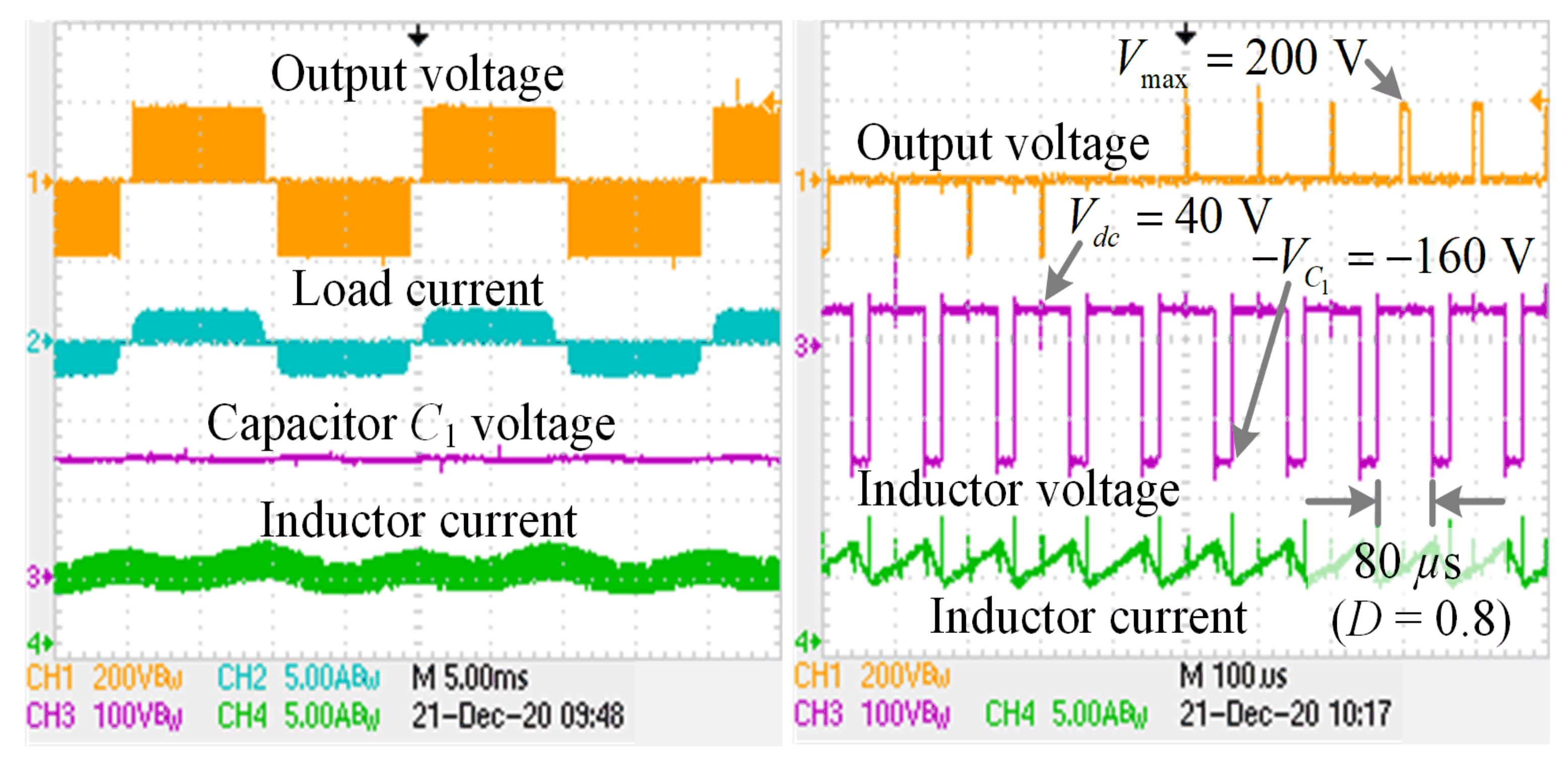
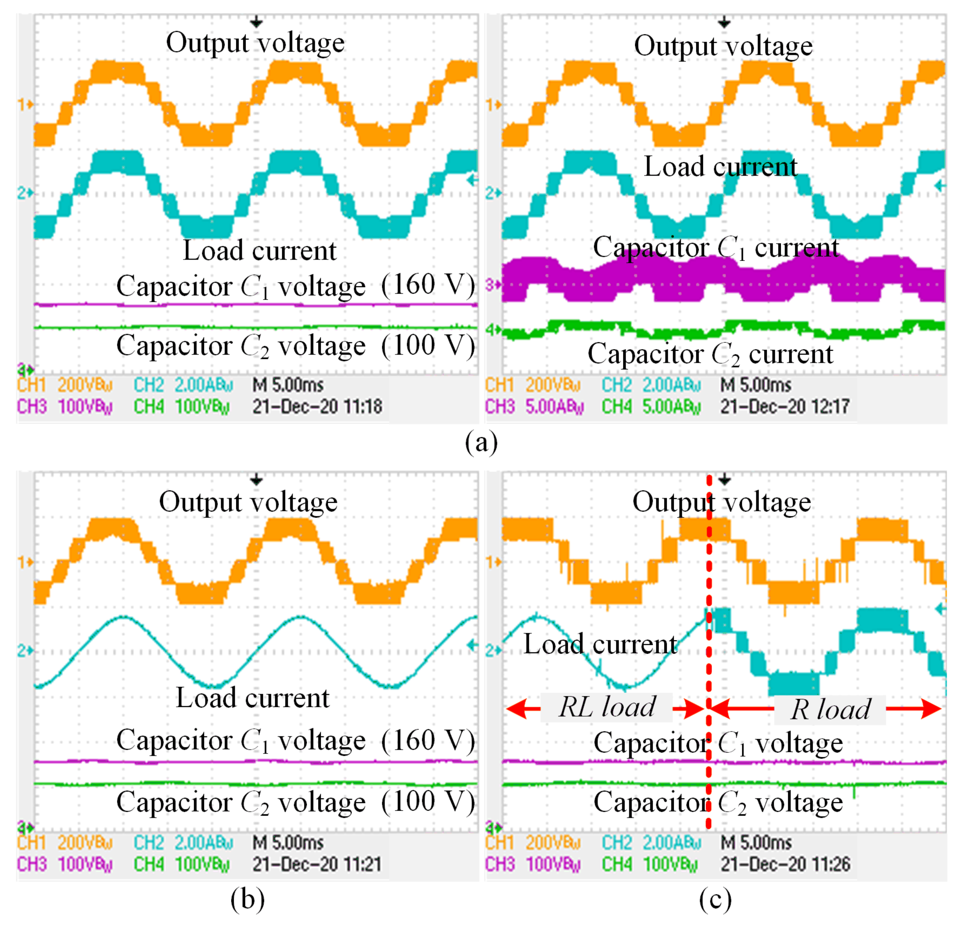
4. Simulation and Experimental Results

For validation, simulations using Matlab Simulink SimPowerSystems toolbox and experimental tests of a prototype depicted in Figure 4 were conducted. The following parameters were considered: Vdc = 40 V, C1 = C2 = 1000 µF, L = 3 mH, fo = 50 Hz, fs = 10 kHz, D = 0.8, load resistance = 100 Ω and load inductance = 100 mH. A power board consisting of silicon carbide power MOSFETs was used to construct the proposed ICHB (3L) and ICHB (5L) according to their schematic, as shown in Figure 1b,c, respectively. An FPGA was used to implement the PWM scheme presented in Figure 3 and generate switching signals for controlling the inverter.
The simulation results of the ICHB (3L) depicted in Figure 5a show that the inductor was charged with a constant D of 0.8 that in turn boosted the capacitor voltage of C1 to 160 V. The maximum voltage level is 200 V. When the capacitor C2 in the ICHB (5L) achieved natural balancing at 100 V, five symmetrical voltage levels were clearly seen between 200 V and −200 V, as shown in Figure 5b. Figure 5c shows the simulation results of the ICHB (5L) when two modules (n = 2) were considered. The number of voltage levels was extended to nine, and it is obvious that the waveforms in each module were identical, thus confirming the modularity feature of the proposed topology.
To investigate the advantage of the proposed topology compared to the conventional CHB, an efficiency study was carried out in Figure 6. The efficiency was computed via simulation by modelling the characteristics of power switches and components. For a fair comparison, the same parameters for both the conventional CHB and the proposed ICHB (5L)were considered. As anticipated, the proposed ICHB (5L) exhibited higher efficiency than the conventional CHB. The efficiency improvement increased with power level. This is attributed to a significant reduction in switch and inductor counts by 42% and 50%, respectively, which reduces conduction loss.
For further validation, measurement results from the experimental prototype are presented in Figure 7 and Figure 8. Good agreement is observed between the experimental results and simulations for both ICHB (3L) and (ICHB (5L), thus validating the operation of the proposed topologies. The steady-state response under an RL load in Figure 8b and transient response from an RL to R load in Figure 8c further confirmed the effectiveness of the proposed ICHB (5L).

5. Conclusions

Two improved CHB topologies capable of three-level and five-level generation are proposed in this paper. Without sacrificing the modularity feature of the classical CHB, the superiority of the proposed topologies lies in their compactness and voltage-boosting capability. The three-level topology is developed by reconstruction of the two-stage CHB structure, which encompasses a front-end boost converter and a rear-end H-bridge. The single-stage structure not only saves one switch but also reduces the capacitor voltage stress. When compared to the CHB with the same voltage gain and level generation, the extended five-level topology offers a further reduction in power switch, an isolated dc source, and inductor counts. Moreover, a significant efficiency improvement is guaranteed. Good agreement is found among the theoretical analysis, simulations, and experimental results. The proposed topologies are suitable for renewable energy applications such as micro inverters for PV system.

Author Contributions

Conceptualization, methodology, writing—original draft preparation, S.S.L.; writing—review and editing, Y.Y., Y.P.S., and R.B. All authors have read and agreed to the published version of the manuscript.

Funding

This research received no external funding.

Conflicts of Interest

The authors declare no conflict of interest.

References

  1. McMurray, W. Fast response stepped-wave switching power converter circuit. U.S. Patent 3581212, 25 May 1971. [Google Scholar]
  2. Akagi, H. Multilevel Converters: Fundamental Circuits and Systems. Proc. IEEE 2017, 105, 2048–2065. [Google Scholar] [CrossRef]
  3. Malinowski, M.; Gopakumar, K.; Rodriguez, J.; Pérez, M.A. A Survey on Cascaded Multilevel Inverters. IEEE Trans. Ind. Electron. 2010, 57, 2197–2206. [Google Scholar] [CrossRef]
  4. Cecati, C.; Ciancetta, F.; Siano, P. A Multilevel Inverter for Photovoltaic Systems with Fuzzy Logic Control. IEEE Trans. Ind. Electron. 2010, 57, 4115–4125. [Google Scholar] [CrossRef]
  5. Rana, R.A.; Patel, S.A.; Muthusamy, A.; Lee, C.w.; Kim, H.-J. Review of Multilevel Voltage Source Inverter Topologies and Analysis of Harmonics Distortions in FC-MLI. Electronics 2019, 8, 1329. [Google Scholar] [CrossRef] [Green Version]
  6. Ye, M.; Ren, W.; Wei, Q.; Song, G.; Miao, Z. Research on Modified Hybrid Frequency Modulation Technology of Type-III Asymmetric CHB Multilevel Inverters. Electronics 2020, 9, 263. [Google Scholar] [CrossRef] [Green Version]
  7. Tayyab, M.; Sarwar, A.; Khan, I.; Tariq, M.; Hussan, M.R.; Murshid, S.; Alhosaini, W. A Single Source Switched-Capacitor 13-Level Inverter with Triple Voltage Boosting and Reduced Component Count. Electronics 2021, 10, 2321. [Google Scholar] [CrossRef]
  8. Vijeh, M.; Rezanejad, M.; Samadaei, E.; Bertilsson, K. A General Review of Multilevel Inverters Based on Main Submodules: Structural Point of View. IEEE Trans. Power Electron. 2019, 34, 9479–9502. [Google Scholar] [CrossRef]
  9. Su, G.J. Multilevel DC-link inverter. IEEE Trans. Ind. Appl. 2005, 41, 848–854. [Google Scholar] [CrossRef]
  10. Hosseinzadeh, M.A.; Sarebanzadeh, M.; Rivera, M.; Babaei, E.; Wheeler, P. A Reduced Single-Phase Switched-Diode Cascaded Multilevel Inverter. IEEE J. Emerg. Sel. Top. Power Electron. 2020, 9, 3556–3569. [Google Scholar] [CrossRef]
  11. Samadaei, E.; Gholamian, S.A.; Sheikholeslami, A.; Adabi, J. An Envelope Type (E-Type) Module: Asymmetric Multilevel Inverters with Reduced Components. IEEE Trans. Ind. Electron. 2016, 63, 7148–7156. [Google Scholar] [CrossRef]
  12. Samadaei, E.; Sheikholeslami, A.; Gholamian, S.A.; Adabi, J. A Square T-Type (ST-Type) Module for Asymmetrical Multilevel Inverters. IEEE Trans. Power Electron. 2018, 33, 987–996. [Google Scholar] [CrossRef]
  13. Alishah, R.S.; Hosseini, S.H.; Babaei, E.; Sabahi, M. Optimal Design of New Cascaded Switch-Ladder Multilevel Inverter Structure. IEEE Trans. Ind. Electron. 2017, 64, 2072–2080. [Google Scholar] [CrossRef]
  14. Lee, S.S.; Lim, C.S.; Siwakoti, Y.P.; Lee, K.B. Dual-T-Type 5-Level Cascaded Multilevel Inverter (DTT-5L-CMI) with Double Voltage Boosting Gain. IEEE Trans. Power Electron. 2020, 35, 9522–9529. [Google Scholar] [CrossRef]
  15. Tran, V.-T.; Nguyen, M.-K.; Ngo, C.-C.; Choi, Y.-O. Three-Phase Five-Level Cascade Quasi-Switched Boost Inverter. Electronics 2019, 8, 296. [Google Scholar] [CrossRef] [Green Version]
  16. Lee, S.S.; Yang, Y.; Siwakoti, Y.P.; Lee, K.B. A Novel Boost Cascaded Multilevel Inverter. IEEE Trans. Ind. Electron. 2021, 68, 8072–8080. [Google Scholar] [CrossRef]
Figure 1. Derivation of the proposed ICHB topologies: (a) classical CHB with a front-end boost converter, (b) proposed ICHB (3L), and (c) proposed ICHB (5L).
Electronics 10 02801 g001
Figure 2. Switching states of the proposed topologies: (a) ICHB (3L) and (b) ICHB (5L).
Electronics 10 02801 g002
Figure 3. Pulse-width modulation scheme for the proposed topologies: (a) ICHB (3L) and (b) ICHB (5L).
Electronics 10 02801 g003
Figure 4. Experimental setup.
Electronics 10 02801 g004
Figure 5. Simulation results of the proposed improved CHB multilevel inverters: (a) single module of 3-level topology (ICHB (3L), n = 1), (b) single module of 5-level topology (ICHB (5L), n = 1), and (c) two cascaded modules of 5-level topology (ICHB (5L), n = 2).
Electronics 10 02801 g005
Figure 6. Efficiency of the proposed ICHB (5L) and comparison with the classical CHB for 5-level generation.
Electronics 10 02801 g006
Figure 7. Experimental results of a single ICHB (3L), n = 1.
Electronics 10 02801 g007
Figure 8. Experimental results of a single ICHB (5L), n = 1: (a) steady-state response under purely resistive R load, (b) steady-state response under series resistive-inductive RL load, and (c) transient response.
Electronics 10 02801 g008
Table 1. Comparison between the proposed ICHBs and the classical CHB with a front-end boost converter (Figure 1a).
3-Level5-Level
CHB
(Figure 1a, n = 1)
Proposed ICHB (3L)CHB
(Figure 1a, n = 2)
Proposed ICHB (5L)
Switch65127
DC source1121
Inductor1121
Capacitor1122
GainM/(1 − D)M/(1 − D)M/(1 − D)M/(1 − D)
V C 1 / V max 1D0.5D
V C 2 / V max 0.50.5
TSV / V max 6566
Gain is the ratio between the peak of the fundamental ac voltage and the total voltage of isolated dc sources.
Publisher’s Note: MDPI stays neutral with regard to jurisdictional claims in published maps and institutional affiliations.

