Article

On-Chip Voltage-Controlled Oscillator Based on a Center-Tapped Switched Inductor Using GaN-on-SiC HEMT Technology

by
Hsuan-Ling Kao
1,2,3
1
Department of Electronic Engineering, Chang Gung University, Tao-Yuan 33302, Taiwan
2
Centre for Reliability Sciences and Technologies, Chang Gung University, Tao-Yuan 33302, Taiwan
3
Department of Dermatology, Chang Gung Memorial Hospital, Linkou Branch, Tao-Yuan 33305, Taiwan
Electronics 2021, 10(23), 2928; https://doi.org/10.3390/electronics10232928
Submission received: 5 November 2021 / Revised: 22 November 2021 / Accepted: 24 November 2021 / Published: 25 November 2021
(This article belongs to the Section Microelectronics)

Abstract

:
This study presents a voltage-controlled oscillator (VCO) in a cross-coupled pair configuration using a multi-tapped switched inductor with two switch-loaded transformers in 0.5 µm GaN technology. Two switch-loaded transformers are placed at the inner and outer portions of the multi-tapped inductor. All the switches are turned off to obtain the lowest sub-band. The outer transformer with three pairs of switches is turned on alternately to provide three sub-band modes. A pair of switches at the inner transformer provide a high-frequency band. Two switch-loaded transformers are turned on to provide the highest sub-band. Six modes are selected to provide a wide tuning range. The frequency tuning range (FTR) of the VCO is 27.8% from 3.81 GHz to 8.04 GHz with a varactor voltage from 13 V to 22 V. At a 1 MHz frequency offset from the carrier frequency of 4.27 GHz, the peak phase noise is −119.17 dBc/Hz. At a power supply of 12 V, the output power of the carrier at 4.27 GHz is 20.9 dBm. The figure of merit is −186.93 dB because the VCO exhibits a high output power, low phase noise, and wide FTR. To the best of the author’s knowledge, the FTR in VCOs made of GaN-based high electron mobility transistors is the widest reported thus far.

1. Introduction

A voltage-controlled oscillator (VCO) is the most ubiquitous element in fully integrated transceivers to generate a tunable local carrier as a local oscillator for up and down frequency conversion in phased array or radar systems [1,2]. To effectively drive multiple mixers in a phased array or provide sufficient detection range for transmitters, AlGaN/GaN high electron mobility transistors (HEMT) are promising candidates for high power at radio-frequency applications. VCOs are the basic element of fifth-generation wireless communication, which can be used in base stations and military applications. The inherent material properties of wide bandgap GaN enable high-power handling capability and better microwave noise performance for low-noise amplifiers and VCOs [3,4]. Furthermore, GaN HEMT on a high-thermal-conductivity SiC substrate provides better reliability for high-power operation. GaN-based monolithic microwave integrated circuits (MMICs) are indispensable in the development of next-generation wireless communication systems.
Research on the design of a high-power MMIC oscillator in GaN HEMT technology has been reported. Fixed-frequency oscillators have been reported to provide a low phase noise (PN) instead of frequency tuning range (FTR) and high efficiency [5,6]. With the demand for the increased capacity of wireless communication systems, VCOs are required to have a wide bandwidth or multiple frequency bands. The most commonly used LC tank in VCOs for frequency tuning is the varactor, which has a low PN and low power consumption. An 8.5–9.5 GHz VCO was designed using 0.15 µm GaN-on-SiC HEMT technology with 31.8 dBm Pout, 11.1% FTR and −101 dBc/Hz PN at the offset of 1 MHz [7]. A common-gate balanced Colpitts VCO operated at 6.45–7.55 GHz was fabricated in 0.25 µm GaN HEMT on silicon carbon substrate with 15% FTR, 2 dBm Pout, and −132 dBc/Hz PN at a 1 MHz offset [8]. A common-source single-end VCO with a feedback network was fabricated using 0.25 µm GaN-on-SiC HEMT technology with 400 MHz FTR, 1.06 dBm Pout, and −122.5 dBc/Hz PN at the offset of 1 MHz [9]. A power VCO based on a T-type lumped-element feedback delay line topology and Class E power amplifier with a frequency from 9.348 GHz to 9.46 GHz was prototyped with 0.25 µm GaN HEMT on SiC, which has 27.9 dBm Pout and −121.62 dBc/Hz PN at the offset of 1 MHz [10]. Although the VCO provides high power and low PN, its FTR is limited by the varactor because the doping profile of GaN HEMT is determined by the epitaxy of transistors. Moreover, the quality factor (Q-factor) of the varactor degrades rapidly with frequency, resulting in a narrow bandwidth. Regarding the wide frequency band, multiband selection is a good approach to extend the bandwidth. Switched capacitor banks or switched inductors are commonly used to obtain a wide tuning range for VCOs [11,12]. However, switched capacitor or switched inductor arrays for GaN technology are hardly applicable because of the large parasitic capacitance and on-resistance of their switches and the large space that they occupy. Wideband multimode magnetically coupled multicore VCOs, which combine the tuning range with multiple modes, have been proposed. However, coupled multicore results in lossy coupled resonators and additional power consumption [13,14]. Tuning frequency via magnetic field has been proposed to increase the tuning range by band selection for single-core VCOs [15,16]. Magnetic tuning is performed by changing the inductance of the primary coil based on the tunable elements in the secondary coil to reduce the significant parasitic effect of the tunable elements, enabling DC noise isolation for the tuning element. In this work, we present a VCO in a cross-coupled pair configuration involving a multi-tapped switched inductor with two switch-loaded transformers. Two switch-loaded transformers providing overlapped tuning ranges are located at the inner and outer portions of the multi-tapped inductor. The tuning range of the fabricated switched inductor VCO is 3.81–5.04 GHz (27.8%). The lowest PN is −119.17 dBc/Hz at a 1 MHz offset at 4.27 GHz, and the highest Pout of 20.9 dBm is obtained at 4.8 GHz using a power supply of 12 V.

2. Circuit Design

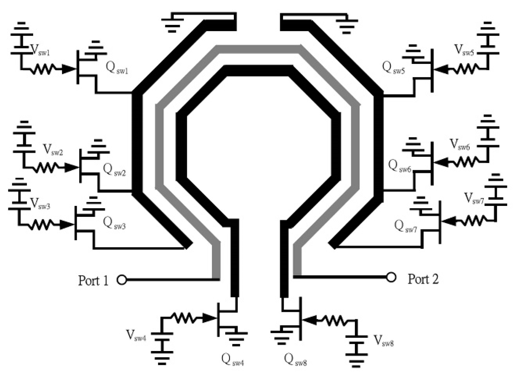
2.1. Switched Inductor

Figure 1 shows the configuration of a conventional loaded transformer-based variable inductor. Lp and Ls represent the primary and secondary coils of the transformer, respectively. Cv and Rv are the variable capacitor and resistor, respectively. Furthermore, k is the coupling factor between coils. When a signal passes through the primary coil, a current is induced in the secondary coil, causing it to generate an induced magnetic field. The induced magnetic field of the secondary coil is opposite to the magnetic field of the primary coil, thus canceling the magnetic field. Thus, the inductance of the primary coil changes, resulting in multiple frequency bands. The variable inductor can be calculated using the input impedance Zin, which is written as follows [17]:
Z i n = j ω L p ( j ω ) 2 M 2 Z o u t + j ω L s
where M is the mutual inductance and Zout is written as follows:
Z o u t = R v 1 + j ω C v R v
By substituting Equation (2) into Equation (1), the equivalent inductance and resistance of the loaded transformer can be derived as follows:
L e q = L p R v 2 [ 1 ω 2 C v L s ( 1 k 2 ) ] 2 + ω 2 L s 2 ( 1 k 2 ) 2 R v 2 ( 1 ω 2 C v L s ) [ 1 ω 2 C v L s ( 1 k 2 ) ] + ω 2 L s 2 ( 1 k 2 )
and
R e q = L p R v 2 [ 1 ω 2 C v L s ( 1 k 2 ) ] 2 + ω 2 L s 2 ( 1 k 2 ) 2 k 2 R v L s
The inductance can be tuned by loading adjustable components, such as varactors, resistors, or switches. The varactor-loaded and switch-loaded components are usually used for transformer-based variable inductors. In this work, a switched inductor is obtained using two switch-loaded transformers to provide overlapping multibands to achieve a wide bandwidth. Figure 2 depicts the equivalent circuit of the switch-loaded transformer at switch on/off. Transistor as a switch can be modelled as R and C in a parallel circuit for both states. Zout at the ON and OFF states can be expressed as RON + 1/(jωCON) and ROFF + 1/(jωCOFF), respectively, where ROFF, COFF, RON, and CON are the equivalent circuit parameters for the switched transistor at the ON and OFF states. Notably, RON is usually smaller than 1/(jωCON) and ROFF is usually larger than 1/(jωCOFF). CON and ROFF can be neglected. Leq at the ON state can be assumed when RON is approaching zero. Substituting Zout into Equation (3), the first term in denominator and numerator of Equation (3) can be neglected and Leq at the ON state can be written as follows:
L e q , O N L p ω 2 L s 2 ( 1 k 2 ) 2 ω 2 L s 2 ( 1 k 2 ) L p ( 1 k 2 )
Leq at the OFF state can be assumed if RON is approaching infinite. Therefore, the second term in denominator and numerator can be neglected; Leq at the OFF state can be written as follows:
L e q , O F F L p R v 2 [ 1 ω 2 C O F F L s ( 1 k 2 ) ] 2 R v 2 ( 1 ω 2 C O F F L s ) [ 1 ω 2 C O F F L s ( 1 k 2 ) ] L p ( 1 + ω 2 L s C O F F k 2 1 ω 2 L s C O F F )
However, the coil area occupied a large space on the chip, resulting in the limitation of the number of transformers. To avoid area expansion and increased bandwidth, two secondary coils are placed inside and outside the primary coil. In this work, the secondary coils are placed at the inner and outer portions of the multi-tapped inductor to provide compact size. Figure 3 shows the proposed layout of the multi-tapped switched inductor with two switch-loaded transformers. The center coil, which is a multi-tapped inductor, is considered the primary coil. Then, more switches are added at inner and outer portions of coils (two secondary coils) to increase the number of sub-bands. The switches are placed at three corners of outer coil and connected between the outer coil and the ground. Only one switch was connected between the edge of the inner coil and the ground. Symmetrical configuration and differential operation can reduce the common mode effects and improve the phase noise. Band selection is used based on the coupling length of the primary and secondary coils. A sub-band is generated when all switches are turned off (Mode 1), which has the largest inductance and the lowest frequency. Three sub-bands are created by turning on the pair of switches on both sides of the outer coil alternately when the switch at the inner coil is turned off (Modes 2–4). The inductance decreases sequentially from Mode 2 to Mode 4 because the coupling length increases accordingly. Mode 5 operates when the switch at the inner coil is turned on and the switches at the outer coil are turned off. The inner coil dominates the coupling ratio to obtain small inductance. The inductance at Mode 5 is smaller than outer coil operates because of its longer coupling length. Only the longest coupling length of the switch (QSW3/QSW6) at the outer coil is turned on when operating with the inner coil (Mode 6). The highest frequency band is obtained because of lowest inductance when inner and outer coupling are both operating. Six modes of sub-bands are selected for the switched inductor. Multiband is created by two switch-loaded transformers to provide continuous sub-bands for width bandwidth. Table 1 summarizes the six modes of sub-bands generated by the switches.

2.2. Design of Switched-Inductor VCO

The topology used conventional cross-coupled VCO involving a switched inductor with two switch-loaded transformers. The LC tank consists of an inductor with two switch-loaded transformers and two varactors (Cv1,2). The losses in the LC tank were compensated by using transistors (Q1,2). C1 and C2 are DC block capacitors because GaN HEMT operates at negative gate bias. R1 and R2 provide a stable gate bias for the core circuit. The widths of the cross-coupled pair of transistors and switch-loaded transistors (Qsw1 ~ Qsw8) are 4 × 100 and 6 × 100 µm, respectively. Two 4 × 100 µm GaN HEMTs were modified by connecting the sources and drains as two-port devices as two varactors (Cv1 and Cv2). The switched inductor VCO was biased at VD = 12 V, VG = −1.2 V, ID = 260–300 mA, and Vtune = 13–22 V. The gate bias of the switch-loaded transistors was 0 V and −5 V for the ON and OFF states, respectively. To ensure balanced signals of the cross-coupled pair in the core circuit, an air bridge is used in GaN MMIC to form a metal crossing to achieve symmetry. Backside ground of wafer and via-hole connection from frontside to backside was used to improve self-heating effect and obtain high gain. The circuit is designed and verified by Advance Design System (ADS) Momentum Electromagnetic simulation to consider signal interference and parasitic effects. The inductor provides coarse tuning via switch-loaded transformers for band selection. Fine-tuning is performed using varactors. The oscillation frequency (fo) of VCO is determined as follows:
f 0 = 1 L e q C e q
where Leq is the equivalent inductance of the LC tank. Here, Ceq includes the varactor capacitance and the parasitic capacitance contributed by cross-coupled pair configuration. Figure 4 depicts the circuit architecture of the designed switched inductor VCO. In this work, the VCO has six continuous sub-bands using a switched inductor. The high power and low PN of VCO are achieved by using highly symmetrical interconnects to balance differential signals.

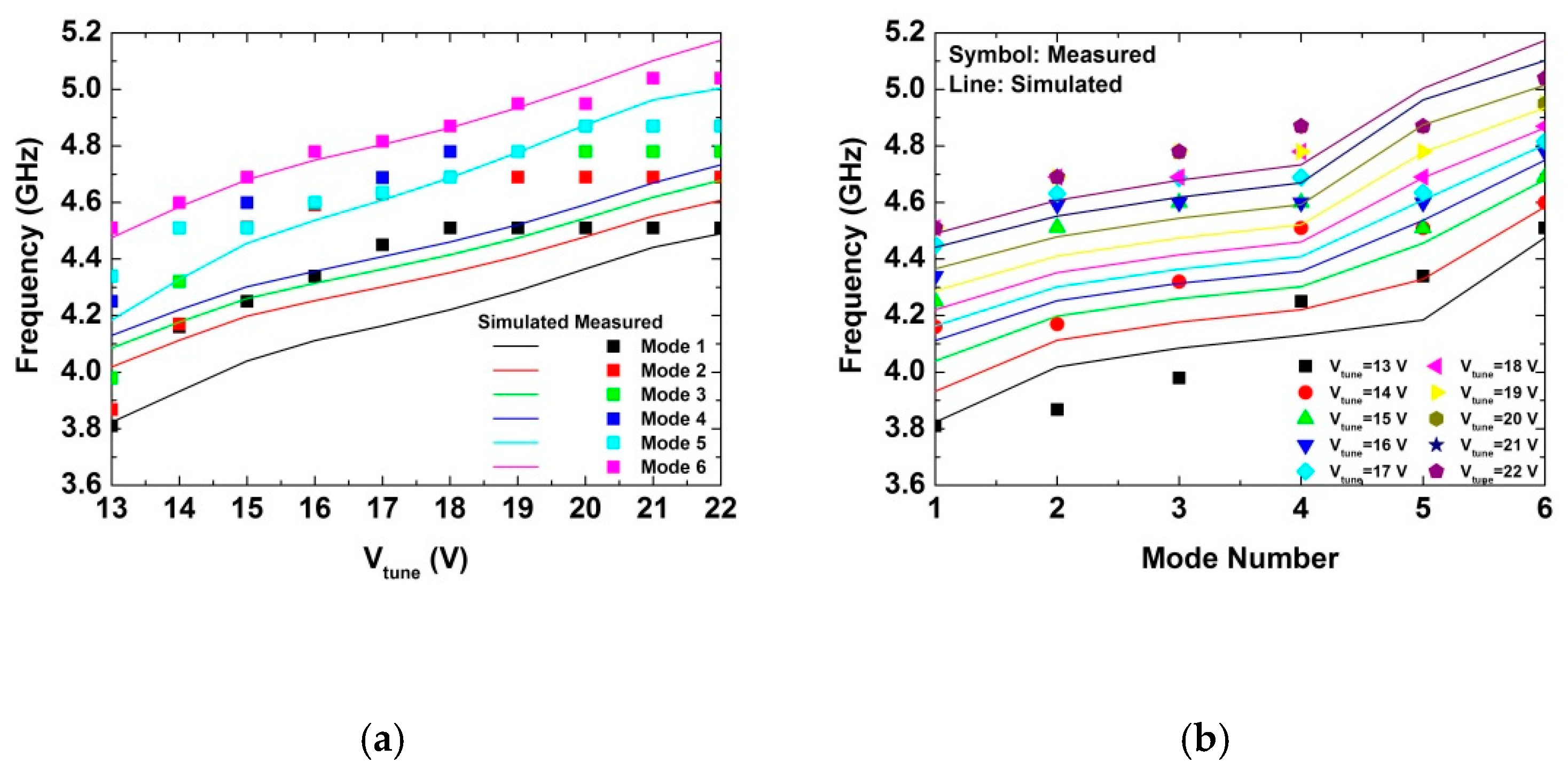
3. Results and Discussion

The switched inductor VCO was characterized using a spectrum analyzer for spectral density and a signal source analyzer for phase noise measurements. Figure 5 shows a photograph of the VCO circuit based on a switched inductor loaded with two transformers. The VCO was implemented using 0.5 µm GaN HEMT on SiC technology with a chip size of 2.2 × 2 mm2 from Transcom, Inc. (Tainan County, Taiwan.) Figure 6 shows the simulated and measured FTR for each sub-band with Vtune varying from 13 V to 22 V. Six continuous sub-bands generate the entire tuning range. Within each sub-band, an FTR of 0.53–0.83 GHz was achieved by the varactors with an FTR of 11.1% to 19.4%. The total tuning range of the proposed VCO was obtained with the oscillation frequency varying from 3.81 GHz to 5.04 GHz, which results in an FTR of 27.8%. The tuning frequency versus each switch mode with Vtune varying from 13 V to 22 V is also shown in the figure. Notably, coarse frequency tuning was dominated by mode numbers, whereas fine-tuning was controlled using varactors, particularly when Vtune > 18 V. Although the outer coil is larger than the inner coil, the coupling lengths of Modes 3–5 are still too close, resulting in a nonlinear crossover between Modes 3–5. All the modes overlap to provide a wide continuous frequency range when Vtune varies from 13 V to 22 V. The tuning range of the simulated and measured results were similar. The difference between the simulated and measured results is due to parasitic effects and the accuracy of the model, particularly in high voltage. Figure 7 shows the measured PN from 1 kHz to 10 MHz offset for each mode. The PN is higher when the switch is turned on because the Q-factor of the inductor is degraded. Mode 1 has less PN because all the switches are in the OFF state. Figure 8a shows the lowest PN of −119.17 dBc/Hz at 1 MHz offset from the carrier frequency of 4.27 GHz. QSWs 3/4 (QSWs 6/8) are turned on at Mode 6, resulting in a high PN. The worst PN of −109.17 dBc/Hz at the offset of 1 MHz from the carrier frequency of 5.04 GHz is detected at Mode 6 because two switches are turned on. The average PN is −114.6 ± 5.3 dBc/Hz at 1 MHz offset for the carrier frequency varying from 3.81 GHz to 5.04 GHz. Figure 9 shows the Pout for all the states. For the output power measurement, one of the output ports is connected to a spectrum analyzer for output power measurement and the other output port is connected by a 50-ohm resistance for balance. The maximum Pout of 20.9 dBm at Mode 5, including 2.9 dB cable loss, is shown in Figure 8b. A large Pout at Modes 1 and 5 is observed because the coupling path connected to the ground is far from VDD. Conversely, Mode 2 has the lowest Pout compared with the other modes because the coupling length is close to VDD, resulting in energy coupling to the ground when SWs 1/4 are turned on. The average Pout for all the modes was 19.4 ± 2.8 dBm. Similar to PN, Pout was degraded when the switched transistor was turned on. A high Pout of VCO indicates a low phase noise, which can be explained using Leeson’s formula, as follows [18]:
( Δ ω ) = 10 log { 2 F K T P s i g [ 1 + ( ω 0 2 Q Δ ω ) 2 ] ( 1 + Δ ω 1 / f 3 | Δ ω | ) }
where (ω) is single side band PN density at the Δω offset of ω0 carrier frequency, Psigis the output power, F is PN figure, Q is the Q-factor of LC tank, Δω1/f3 is the 1/f3 corner frequency, K is the Boltzman constant, and T is the temperature. The performance of the proposed VCO and those reported in previous literature [7,9,10,19] are summarized in Table 2. The figure of merit (FOMT), which is employed to investigate their advantages, is defined as follows [20]:
FOM T = 20 log ( f 0 f o f f s e t T R % 10 ) { f o f f s e t } + 10 log ( P o u t P D C )
where {foffset} is the measured PN at the foffset offset of f0 carrier frequency. TR%, PDC, and Pout are the percentage of FTR, dc power consumption, and output power, respectively. A large FOMT corresponds to an oscillator with high output power, wide bandwidth, and low PN. The fabricated VCO is compared with most state-of-the-art works. The highest FOMT was obtained in this work using a wide tuning range, high power, and low PN. Switch inductance by transformer loading provides a wide tuning range for millimeter-wave VCOs, particularly for high-power operation.

4. Conclusions

In this study, a switched inductor was tuned by two switch-loaded transformers for a VCO in a cross-coupled pair configuration. Using the proposed frequency tuning scheme, the VCO was realized in 0.5 µm GaN HEMT on SiC technology with design goals for the maximum FTR, low PN, and high Pout. The measured results show that the VCO achieved an FTR of 27.8% from 3.81 GHz to 8.04 GHz with a maximum Pout of 20.9 dBm. With a 1 MHz frequency offset, the PN varied from −109.2 dBc/Hz to −119.17 dBc/Hz across the six sub-bands. The proposed VCO has a strong potential to be integrated into fifth-generation wireless base stations and military systems.

Funding

This work was supported by the Ministry of Science and Technology, Taiwan (no. 109-2221-E-182-027 & no. 110-2221-E-182-057-MY2) and the Chang Gung Memorial Hospital, Taiwan (BMRP957 & CMRPD2K0042).

Data Availability Statement

The data presented in this study are available in article.

Acknowledgments

The authors thank the Centre for Reliability Sciences and Technologies at Chang Gung University for their help. This work was supported by the Chang Gung Memorial Hospital, Taiwan (BMRP957 & CMRPD2K0042).

Conflicts of Interest

The author declares no conflict of interest.

References

  1. Hejazi, A.; Pu, Y.; Lee, K.-Y. A Design of Wide-Range and Low Phase Noise Linear Transconductance VCO with 193.76 dBc/Hz FoMT for mm-Wave 5G Transceivers. Electronics 2020, 9, 935. [Google Scholar] [CrossRef]
  2. Mghabghab, S.R.; Nanzer, J.A. Impact of VCO and PLL Phase Noise on Distributed Beamforming Arrays with Periodic Synchronization. IEEE Access 2021, 9, 56578–56588. [Google Scholar] [CrossRef]
  3. Florian, C.; Traverso, P.A.; Santarelli, A. Ka-Band MMIC LNA in GaN-on-Si 100-nm Technology for High Dynamic Range Radar Receivers. IEEE Microw. Wirel. Compon. Lett. 2021, 31, 161–164. [Google Scholar] [CrossRef]
  4. Kong, C.; Li, H.; Chen, X.; Jiang, S.; Zhou, J.; Chen, C. Monolithic AlGaN/GaN HEMT VCO Using BST Thin-Film Varactor. IEEE Trans. Microw. Theory Tech. 2012, 60, 3413–3419. [Google Scholar] [CrossRef]
  5. Liu, H.; Zhou, X.; Boon, C.C.; Yi, X.; Mao, M.; Yang, W. Design of Ultra-Low Phase Noise and High Power Integrated Oscillator in GaN-on-SiC HEMT Technology. IEEE Microw. Wirel. Compon. Lett. 2014, 24, 120–122. [Google Scholar] [CrossRef]
  6. Lai, S.; Kuylenstirena, D.; Özen, M.; Hörberg, M.; Rorsman, N.; Angelov, I.; Zirath, H. Low Phase Noise GaN HEMT Oscillators with Excellent Figures of Merit. IEEE Microw. Wirel. Compon. Lett. 2014, 24, 412–414. [Google Scholar] [CrossRef]
  7. Kaper, V.; Thompson, R.; Prunty, T.; Shealy, J.R. X-band AlGaN/GaN HEMT MMIC voltage-controlled oscillator. In Proceedings of the 11th Gallium Arsenide applications Symposium, Munich, Germany, 6–7 October 2003; pp. 45–48. [Google Scholar]
  8. Thanh, N.T.D.; Lai, S.; Hörberg, M.; Zirath, H.; Kuylenstierna, D. A MMIC GaN HEMT voltage-controlled-oscillator with high tuning linearity and low phase noise. In Proceedings of the 2015 IEEE Compound Semiconductor Integrated Circuit Symposium, New Orleans, LA, USA, 11–14 October 2015. [Google Scholar]
  9. Jang, S.-L.; Chang, Y.-H.; Lai, W.-C. A feedback GaN HEMT oscillator. In Proceedings of the 2018 International Conference on Microwave and Millimeter Wave Technology, Chengdu, China, 7–11 May 2018. [Google Scholar]
  10. Chuang, C.-C.; Chiou, H.-K. A low phase noise X band class E power VCO in 0.25 μm GaN/SiC technology. In Proceedings of the 2021 IEEE International Symposium on Radio-Frequency Integration Technology, Hualien, Taiwan, 25–27 August 2021. [Google Scholar]
  11. Mukhopadhyay, R.; Lee, C.-H.; Laskar, J. A 580-μW 1.8–6 GHz Multiband Switched-Resonator SiGe VCO with 0.3-V Supply Voltage. IEEE Microw. Wirel. Compon. Lett. 2007, 17, 793–795. [Google Scholar] [CrossRef]
  12. Jang, S.-L.; Huang, J.-F.; Lin, Y.-S.; Chang, C.-W. Switched inductor dual-band CMOS cross-coupled VCO. Analog Integr. Circuits Signal Process. 2013, 74, 527–532. [Google Scholar] [CrossRef]
  13. Vigilante, M.; Reynaert, P. A Dual-band E-band quadrature VCO with switched coupled transformers in 28nm HPM bulk CMOS. In Proceedings of the 2015 IEEE Radio Frequency Integrated Circuits Symposium, Phoenix, AZ, USA, 17–19 May 2015. [Google Scholar]
  14. Basaligheh, A.; Saffari, P.; Filanovsky, I.M.; Moez, K. A 65–81 GHz CMOS Dual-Mode VCO Using High Quality Factor Transformer-Based Inductors. IEEE Trans. Microw. Theory Tech. 2020, 67, 4533–4543. [Google Scholar] [CrossRef]
  15. Chen, Z.; Che, J.-X.; Yan, P.; Hou, D.; Zhu, F. K-Band Low Phase Noise VCO Based on Q-Boosted Switched Inductor. Electronics 2019, 8, 1132. [Google Scholar] [CrossRef] [Green Version]
  16. Fei, W.; Yu, H.; Fu, H.; Ren, J.; Yeo, K.S. Design and Analysis of Wide Frequency-Tuning-Range CMOS 60 GHz VCO by Switching Inductor Loaded Transformer. IEEE Trans. Circuits Syst. I 2014, 61, 699–711. [Google Scholar] [CrossRef]
  17. Lu, T.-Y.; Yu, C.-Y.; Chen, W.-Z.; Wu, C.-Y. Wide Tunning Range 60 GHz VCO and 40 GHz DCO Using Single Variable Inductor. IEEE Trans. Circuits Syst. I 2013, 60, 257–267. [Google Scholar] [CrossRef]
  18. Leeson, D.B. A simple model of feedback oscillator noise spectrum. Proc. IEEE 1966, 54, 329–330. [Google Scholar] [CrossRef] [Green Version]
  19. Jang, S.-L.; Chang, Y.-H.; Chiou, J.-S.; Lai, W.-C. A single GaN HEMT oscillator with four-path inductors. In Proceedings of the 2018 International Symposium on Next-Generation Electronics, Taipei, Taiwan, 7–9 May 2018. [Google Scholar]
  20. Kim, D.; Jeon, S. W- and G-Band GaN Voltage-Controlled Oscillators with High Output Power and High Efficiency. IEEE Trans. Microw. Theory Tech. 2021, 69, 3908–3916. [Google Scholar] [CrossRef]
Figure 1. Configuration of a conventional loaded transformer-based variable inductor.
Electronics 10 02928 g001
Figure 2. Equivalent circuit of the switch-loaded transformer at switch on/off.
Electronics 10 02928 g002
Figure 3. Layout of the multi-tapped switched inductor with two switch-loaded transformers.
Electronics 10 02928 g003
Figure 4. Complete schematic of the switched inductor VCO with two transformers.
Electronics 10 02928 g004
Figure 5. Photograph of the switched inductor VCO.
Electronics 10 02928 g005
Figure 6. Simulated and measured frequency tuning range versus (a) varactor biases and (b) selection modes for the switched inductor VCO.
Electronics 10 02928 g006
Figure 7. Measured phase noise versus (a) varactor biases and (b) selection modes for the switched inductor VCO.
Electronics 10 02928 g007
Figure 8. Measured (a) PN at the carrier frequency of 4.27 GHz and (b) Pout at 4.8 GHz of the switched inductor VCO.
Electronics 10 02928 g008
Figure 9. Measured output power versus (a) varactor biases and (b) selection modes for the switched inductor VCO.
Electronics 10 02928 g009
Table 1. Six modes of sub-bands for the switched inductor.
ModeQSW1/QSW5QSW2/QSW6QSW3/QSW7QSW4/QSW8
Mode 1OFFOFFOFFOFF
Mode 2ONOFFOFFOFF
Mode 3OFFONOFFOFF
Mode 4OFFOFFONOFF
Mode 5OFFOFFOFFON
Mode 6OFFOFFONON
Table 2. Comparison of MMIC GaN HEMT VCO.
Ref.Technologyf0
(GHz)
Tuning Range
(%)
PN @ 1MHz (dBc/Hz)Pout (dBm)FOMT
[7]0.15 μm HEMT GaN-on-SiC91 GHz (11.1%)−10120.2−174
[9]0.25 μm HEMT GaN-on-SiC7.28400 MHz (5.5%)−122.51.06−182.9
[10]0.25 μm HEMT GaN-on-SiC *71.1 GHz (15.7%)−13227.9−179.1
[19]0.25 μm HEMT GaN-on-SiC2.66145 MHz (5.6 %)−12917.55−177.9
This Work0.5 μm HEMT GaN-on-SiC4.421.23 GHz (27.8%)−119.1720.9−186.9
* including power amplifier.
Publisher’s Note: MDPI stays neutral with regard to jurisdictional claims in published maps and institutional affiliations.

