Article

Optimal Load Determination of Capacitor–Inductor Compensated Capacitive Power Transfer System with Curved-Edge Shielding Layer

1
School of Marine Science and Technology, Northwestern Polytechnical University, Xi’an 710072, China
2
School of Electrical Engineering, Southwest Jiaotong University, Chengdu 610036, China
3
Department of Electrical and Electronic Engineering, The University of Auckland, Auckland 1010, New Zealand
*
Author to whom correspondence should be addressed.
Electronics 2021, 10(23), 2961; https://doi.org/10.3390/electronics10232961
Submission received: 21 October 2021 / Revised: 25 November 2021 / Accepted: 25 November 2021 / Published: 28 November 2021
(This article belongs to the Section Power Electronics)

Abstract

:
Due to the natural low permittivity in vacuum, the voltage stresses on compensation capacitors and inductances in the capacitive power transfer (CPT) system are very high, which brings challenges to the design of CPT systems in practical applications. This paper used a three-cell structure analysis method for the CPT system to determine the optimal load for achieving the maximum power transfer or maximum efficiency transfer, through considering the maximum withstand voltage of the capacitor or inductor. A shielding layer with edge bending is designed to reduce the range of dangerous areas markedly. The simulation and experimental results verified the above conclusion. The prototype of the CPT system with transfer 3.1 kW across a 13 cm air gap and DC-DC transfer efficiency of 91.4% is built.

1. Introduction

The capacitive power transfer (CPT) technology is widely used in many applications, such as medical treatment, transportation, and household appliances [1,2,3,4,5,6,7,8,9]. Compared to the inductive power transfer (IPT) system [10,11,12], the CPT system wirelessly transfers power through electric field coupling, with the advantages of low cost, low eddy current loss, and low sensitivity to foreign objects, and it is not affected by water and other chemicals.
In order to transfer energy through metal barriers, W. Zhou generated an exciting current on a primary aluminum plate and collected the electromagnetic energy by a secondary pickup coil [13]. L. J. Zou proposed a single-wire CPT system, which requires only a single pair of electric coupling plates without a current return path, and allows a large coupling tolerance compared to the traditional CPT systems with two pairs of coupling [14]. Y. Su proposed an F-type CPT compensation network to reduce the voltage stress on the inverter switches and other circuit components when the energy pickup moves into or out of the charging area [15].
The CPT technology is also used in high power electric vehicle charging. F. Lu proposed a bilateral LCLC compensated CPT system to transfer 2.4 kW, with a DC-DC transfer efficiency of 90.8% [16], and also proposed a CLLC topology structure with reduced compensation inductor to transfer 2.57 kW at 89.3% efficiency [17]. H. Zhang proposed a six-plate structure to reduce the electric field radiation, when a transfer power of 1.97 kW and a transfer efficiency of 91.6% are achieved [18]. I. Ramos proposed a distributed near-field phased array to achieve a higher power density with a reduced external radiation range [19]. B. Regensburger proposed a phase-controlled CPT system to improve the shielding performance, by using the parasitic capacitance effect of the shielding layer [20]. Hua Zhang proposed an improved design methodology of the double-sided LC-compensated CPT system considering the inductance detuning, which shows that the inductance detuning has the benefit to achieve the soft-switching condition for the CPT system, and the output current and internal voltage stresses can also be maintained within the desired range [21,22,23]. Fabio Corti presents a complete design methodology of a Class-E inverter for capacitive wireless power transfer applications, focusing on the capacitance coupling influence [24].
The above research works built a good foundation for designing and analyzing the CPT system. However, in practical applications, since the medium is air and the dielectric constant is small, when the transfer distance is large, the coupling capacitance is usually several tens pF, which is small. In order to carry out high-power transfer, it is necessary to increase the resonance frequency and the voltage on the plate. The CPT system is very sensible to parameters due to high Q value, so further research is needed in the aspects of working mechanism, systematic analysis method, reduced voltage stress, and determination of optimal load impedance.
Although many compensation topologies were proposed, such as LCLC, LCL and LC, double-sided capacitor–inductor (CL) compensation topology can also achieve high power and long-distance power transfer, and simplify the compensation topology [25]. Like IPT system, the CPT system can also support the optimal load to achieve the maximum power transfer or maximum efficiency transfer. During high-power electric energy transmission, a strong electric field will be generated around the coupler in the CPT system. Suziana Ahmad designed a structure to reduce the electric field around the system [26]. In this paper, the optimal load is discussed in detail, and a shielding layer with edge bending is designed to reduce the range of dangerous areas. The rest of the article is organized as follows: The second section includes a general circuit topology analysis method for the compensation network of CPT system. In the third section, the determination of the optimal loads with maximum transfer power and maximum transfer efficiency is presented. The fourth section proposes a shielding layer with edge bending. The fifth section is the experimental verification, and conclusions are made in the sixth section.

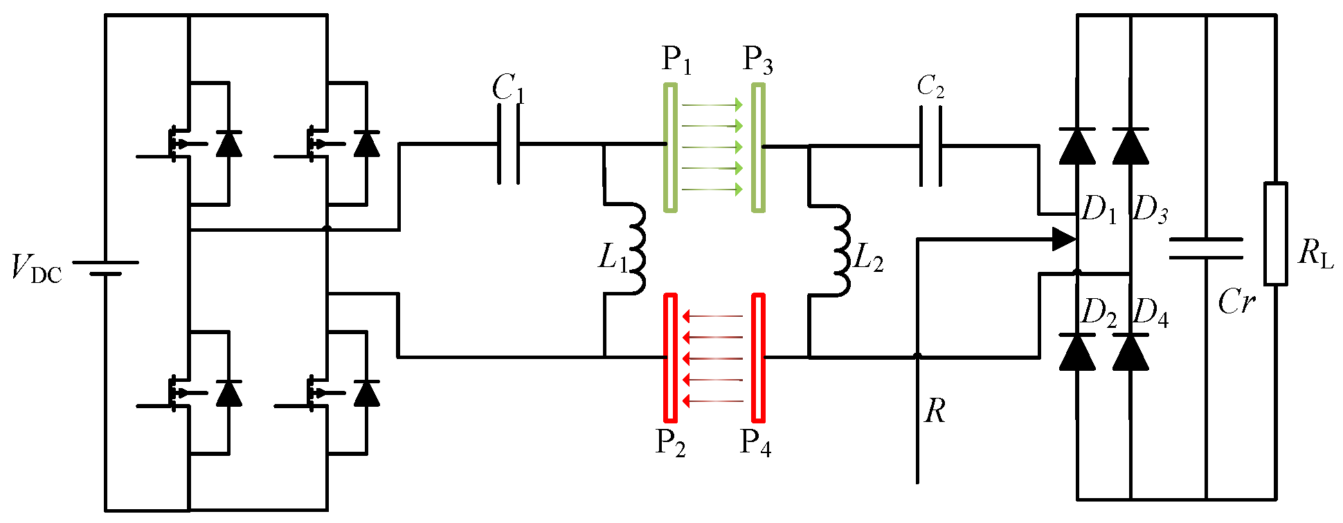
2. General Circuit Topology Analysis for CPT System

In general, the CPT system consists of an inverter, primary side compensation network, two pair of coupling plates, secondary side compensation network, a rectifier, and the load, as shown in Figure 1. The primary side compensation network is composed of L1 and C1, and the secondary side compensation network is composed of L2 and C2. Both compensation networks are CL impedance matching structures. The compensation network in primary side connected to the plates P1, P2 is a voltage gain network, amplifying the voltage from power source to provide high voltage to plates in primary side. Moreover, the compensation network in secondary side connected to the plates P3, P4 is a current gain network, which converts the high voltage on the plates P3 and P4 into the current of the load. A full-bridge rectifier is used to get DC power to change batteries from AC current in the resonant coupling plate.
The CPT system uses electric field coupling to transfer energy, and is usually working at high frequency and high voltage to achieve more transfer power. The value of the resonant frequency should not be too large, because the excessive resonant frequency increases the loss in compensation inductance, the difficulty of realization, and loss in the inverter and the rectifier, which may reduce the system efficiency. After the transfer distance and the coupling structure are determined, the coupling capacitor value is settled. The only thing that can be done is to increase the voltage on the equivalent capacitor. A boost network can be added to increase the voltage between the plates to achieve the wireless transfer of high-power electric energy. The CPT system can be simplified to the three-cell structure, as shown in Figure 2 [13,14,15].
In Figure 2, Z2 and Z3 are impedance including parasitic capacitance, Z1 and Z4 are external series impedances. Generally, in high efficiency network, for ease of analysis, the capacitance and inductance losses are often neglected, and Figure 2 can be simplified as Figure 3.
In Figure 3, X1, X2, X3, and X4 are pure reactance, and X 1 < 0 , X 2 > 0 , X 3 > 0 , X 4 < 0 , X 5 < 0 , X 1 = X 4 , X 2 = X 3 . I1, I2, and I3 are the currents of network 1, network 2, and network 3, respectively, and X5 = −1/ωCM. According to the Kirchhoff voltage, (1), (2) and (3) are obtained:
I 1 j ( X 1 + X 2 ) I 2 j X 2 U = 0
I 2 j ( X 2 + X 3 + X 5 ) I 1 j X 2 I 3 j X 3 = 0
I 3 j ( X 3 + X 4 + R ) I 2 j X 3 = 0
By defining T1 = j(X1 + X2), T2 = jX2, T3 = j(X2 + X3 + X5), T4 = jX3, T5 = j(X3 + X4) and U = [U, 0, 0], the above equations can be expressed as:
U = [ T 1 T 2 0 T 2 T 3 T 4 0 T 4 T 5 + R ] [ I 1 I 2 I 3 ]
Primary and secondary circuits are designed to be symmetrical, in order to simplify calculations. Therefore, T1 = T5, and T2 = T4. The impedance matrix Z can be expressed as:
Z = [ T 1 T 2 0 T 2 T 3 T 2 0 T 2 T 1 + R ]
Based on (5), the admittance matrix Y is
Y = Z 1 = 1 | Z | | ( T 1 T 3 T 2 2 ) + T 3 R T 1 T 2 + T 2 R T 2 2 T 1 T 2 + T 2 R T 1 2 + T 1 R T 1 T 2 T 2 2 T 1 T 2 T 1 T 3 T 2 2 |
where |Z| = T1(T1T3 − 2T22) + (T1T3T22)R.
The equivalent input impedance Zin of the power supply is:
Z i n = T 1 ( T 1 T 3 2 T 2 2 ) + ( T 1 T 3 T 2 2 ) R ( T 1 T 3 T 2 2 ) + T 3 R
The real and imaginary parts of Zin are:
Re ( Z i n ) = R [ ( T 1 T 3 T 2 2 ) 2 T 1 T 3 ( T 1 T 3 2 T 2 2 ) ] ( T 1 T 3 T 2 2 ) 2 ( T 3 R ) 2
Im ( Z i n ) = ( T 1 T 3 T 2 2 ) [ T 1 ( T 1 T 3 2 T 2 2 ) T 3 R 2 ] ( T 1 T 3 T 2 2 ) 2 ( T 3 R ) 2
The numerator of (9) is a product of two terms, and the latter is related to the load. Since the load impedance is variable, the former should be zero, and the condition of T1T3 = T22 can be derived to make the imaginary part of the equivalent input impedance zero.
Z i n = Re ( Z i n ) = R [ T 2 2 ( T 2 2 ) ] ( T 3 R ) 2 = T 2 4 T 3 2 R = T 1 2 R = ( X 1 + X 2 ) 2 R
The resonance condition is:
2 X 1 X 2 + X 1 X 5 + X 2 2 + X 2 X 5 = 0
Based on (4) and (6), the currents I1, I2 and I3 can be expressed as:
I 1 = U T 3 R T 1 T 2 2 = R ( X 1 + X 2 ) 2 U
I 2 = T 1 T 2 + T 2 R T 1 T 2 2 U = R ( X 1 + X 2 ) X 2 U + j X 2 U
I 3 = T 2 2 U T 1 T 2 2 = j ( X 1 + X 2 ) U
Assuming that the external compensating capacitance is C, and the coupling coefficient is defined as kc = CM/C. Based on (11), the corresponding inductance value of the CL compensation structure is obtained as:
L C L = 2 + 1 k C 4 + 1 k C 2 2 ω 2 C = 2 k C + 1 4 k C 2 + 1 2 ω 2 C M
The compensation inductance of the CL structure has two solutions, and one which is ignored here is many times larger than the other one, as shown in (15).

3. The Optimal Load Determination

Due to the natural low permittivity in vacuum, the coupling capacitance in CPT is normally very small, so the voltage stresses on coupling capacitors and compensation inductance are very high, which hinders the practical applications of CPT system widely. When the compensation structure is determined, the only variable parameter of the system is the load impedance. The change of the load affects the maximum output power and efficiency of the system. In practical applications, it is useful to consider the maximum withstand voltage of the capacitor, or inductor to obtain the range of the load, in which the optimal load can be determined to obtain maximum output power or maximum output efficiency.
From (12)–(14), the corresponding voltage values of X1, X2, X3 and X4 can be expressed as:
U X 1 = j X 1 R ( X 1 + X 2 ) 2 U
U X 2 = j X 2 R ( X 1 + X 2 ) 2 U j R X 1 + X 2 U + U
U X 3 = X 2 X 1 + X 2 U + j R X 1 + X 2 U U
U X 4 = X 1 X 1 + X 2 U
Suppose the maximum withstanding voltage of the capacitor and inductor are UC and UL, and the amplitude of the source voltage is Um. Generally speaking, UC > Um and UL > Um. According to (16)–(19), the following relation can be obtained.
X 1 R ( X 1 + X 2 ) 2 U C U m
1 + X 1 2 R 2 ( X 1 + X 2 ) 4 U U L U m
X 1 2 ( X 1 + X 2 ) 2 + R 2 ( X 1 + X 2 ) 2 U L U m
X 1 X 1 + X 2 U C U m
According to (23), in order to avoid the capacitor voltage exceeding the breakdown voltage, the relation between X1 and X2 must meet the following conditions:
{ X 2 X 1 U C + U m U C , I f   ( X 1 + X 2 ) > 0 X 2 X 1 U C U m U C , I f   ( X 1 + X 2 ) < 0
Based on the above limitations (20)–(22), the load R must satisfy the following condition:
{ R U C U m ( X 1 + X 2 ) 2 X 1 R U L 2 U m 2 U m 2 ( X 1 + X 2 ) 4 X 1 2 R U L 2 U m 2 ( X 1 + X 2 ) 2 X 1 2
Considering the maximum withstand voltage of the capacitor or inductor, the parameters of CPT system must meet (24), and the range of the load satisfies:
R M i n { U C U m ( X 1 + X 2 ) 2 X 1 , U L 2 U m 2 U m 2 ( X 1 + X 2 ) 4 X 1 2 , U L 2 U m 2 ( X 1 + X 2 ) 2 X 1 2 }

3.1. Optimal Load for Maximum Power Transfer

The load power can be expressed as:
P L = I 3 2 R
From (14), I3 is independent of load, therefore the load should take the minimum of the three critical values in (25), to obtain maximum power transfer:
R = M i n { U C U m ( X 1 + X 2 ) 2 X 1 , U L 2 U m 2 U m 2 ( X 1 + X 2 ) 4 X 1 2 , U L 2 U m 2 ( X 1 + X 2 ) 2 X 1 2 }

3.2. Optimal Load for Maximum Transfer Efficiency

The above analysis assumes that the compensation network and the equivalent capacitance are purely resistant, but in the practical applications, both the inductor and the capacitor have losses. Because the presence of inductance and capacitance losses is very small and has less effect on the current value in the circuit, the system efficiency is analyzed by the perturbation method [20]. Based on (12)–(14), the power loss on X 1 and X 4 is P X 1 , the power loss on X 2 and X 3 is P X 2 , and the power loss on C M is P M .
P X 1 = ( U 2 R 2 T 1 4 U 2 T 1 2 ) R X 1
P X 2 = [ ( U R T 1 T 2 U R T 1 2 ) 2 U 2 T 2 2 + ( U R T 1 T 2 ) 2 ( U T 2 U T 1 ) 2 ] R X 2
P M = [ ( U R T 1 T 2 ) 2 U 2 T 2 2 ] R M
where R X 1 , R X 2 and R M are parasitic equivalent series resistances of X 1 , X 2 and C M , respectively. The total power loss P l o s s is:
P l o s s = P X 1 + P X 2 + P M
Load power is
P L = U 2 R T 1 2
The efficiency expression of the system is
η = P L P L + P l o s s = 1 1 + P l o s s P L = 1 1 + R T 1 2 G η + G η R
where Gη satisfies:
G η = R X 1 + [ T 1 2 T 2 2 + ( T 1 T 2 1 ) 2 ] R X 2 + T 1 2 T 2 2 R M
If R = jT1 meets the constraints of (26), system efficiency is maximum when R = jT1. At this point, the efficiency η can be expressed as:
η = P L P L + P l o s s = 1 1 + P l o s s P L = 1 1 + 2 [ R X 1 j T 1 + R X 2 ( 1 j T 1 + 2 T 1 j T 2 2 2 j T 2 ) + R M T 1 j T 2 2 ]
If R = jT1 does not meet the constraints of (26), the load should take the minimum of the three critical values in (25) to obtain maximum efficiency transfer.

4. Layer Design of Edge Bending

The optimal load improves the system efficiency, but the radiation is very large during the application. This chapter discusses methods of reducing radiation.

4.1. A Circuit Topology Improvement

Figure 4 is a CL compensation structure, where Z05 and Z06 represent the capacitive reactance between the shield plates P5, P6 and the ground, respectively.
In Figure 4, Capacitors CP, CS and CPS are equivalent capacitances regardless of the shielding layer, respectively, which are equivalent to Cin1-CM, Cin2-CM and 2CM in [21]. It can be judged by geometry that C16 = C35 = C45 = C26, C15 = C25 = C36 = C46, which are the parasitic capacitance between the plate and the shielding layer. The sum of the imaginary part of the voltage on capacitor C1 and inductor L1 is equal to zero, therefore, there exists voltage between P1 and P2; when P2 is grounded, the potential on P5 is not zero. Hence, a potential difference is generated between the shielding layer and ground. Then, I05 will not be zero, which means that the shielding plate cannot shield the electric field. When C1 and C2 are equally uniformly placed on the upper and lower sides of the primary side and the secondary side, the voltage potential on P5 and P6 will be zero, which means that the shielding plates will work [27]. In this case, the equivalent capacitance between the plates is the same as that in [28]. The simplified equivalent circuit diagram is shown in Figure 5.

4.2. Shield Structure Optimization Design

According to the IEEE C95.1-2000 standard, the maximum electric field strength that humans can withstand is 614 V/m. The dangerous area still exists on both sides of the shielding plate in [16], and they are expanded into two big hemispheres, which will threaten human safety. In this paper, the structure of the shielding layer is optimized to shrink the dangerous area. It should be noted that the simulations are for the case of symmetric compensation structures.
The curved structure of the shielding layer has little effect on the equivalent capacitance between the plates. The dimensions of the plate used in the simulation are displayed in Table 1. The corresponding relationship of the parameters is shown in Figure 6. The size of four small plates is exactly the same, and the two big plates are shielding layers.
The structure of the shielding layer can be bent downward to decrease the dangerous area. The relative potential between two shielding layers is always equal to zero during charging. In order to minimize the radiation and not to occupy too much installation volume, the edge of the ordinary six-plate shield structure can be extended to the inside in an arc shape, parallel to the transfer plate. The radius of the arc is the distance between the transfer plate and the shielding layer. So, as a whole, only 1/4 of the circle is extended to the inside. The material of the plates is aluminum. The optimized plate structure is shown in Figure 7.
When the transmission power is 2000 W, and the transmission distance is 130 mm, the electric field cloud diagrams of the two shielding layer structures are shown in Figure 8.
The red in Figure 8 indicates the dangerous area, and its electric field value is greater than 614 V/m. When the transmission power is 2000 W, compared to Figure 8a, the red danger zone in Figure 8b is greatly reduced. It can be seen that the shielding layer with edge bending structure has a better shielding effect.
If V0 is defined as the distance between the shielding plates multiplied by the area of one shielding plate without considering its thickness, and the space volume of the dangerous area (abs(E) ≥ 614 V/m) is taken as the numerator Vd; the shielding effect is calculated by the proportional relationship β = Vd/V0, as shown in Figure 9. It can be seen that the optimized shielding layer structure reduces the dangerous area greatly.

5. Experiment Verification

Since the compensation network is a symmetric network, only the primary side circuit structure is analyzed. Because L1 and CPC are parallel structures, they are equivalent to a capacitor or an inductor, which depend on the magnitude of L1 and CPC. In CL compensation network, it needs to be equivalent to an inductor. The equivalent inductance value is defined as L , then the following expression is established.
j ω L = 1 1 j ω L 1 + j ω C P C
where
L = L 1 1 ω 2 C P C L 1
when ω2CPC L1 < 1, the system can work normally under the CL compensation structure.
The external compensation capacitor value is set to C1 = C2 = 220 pF, and the (15) can be used to obtain L′ = 160.11 uH, so the compensation inductance L1 = L2 = 114.28 uH can be calculated by using (38). L1 is set to be 112 uH, in order to achieve soft switch so that it emproves the efficiency of the inverter. System parameters are shown in Table 2.
RL is the equivalent impedance of batteries. For a high-efficiency rectifier, the values of the equivalent AC load value and the DC impedance satisfy the following relationship [29]:
R = 8 π 2 R L
The optimal load for maximum efficiency transfer is R ≈ 67.76 Ω, which meets the constraints of (26). The compensation capacitor is welded by the unit capacitor PHE448 330 pF polypropylene film capacitor. C1 and C2 are respectively composed of two sets of capacitors, which are respectively connected in series between the inverter and the equivalent resistor in Figure 5. In order to reduce the skin effect of the wire on the compensation inductor, the compensation inductor is wound by 2500 AWG44 Leeds wire, and the Q value of the compensation inductor is 1170. In order to obtain high voltage and high frequency capacitance, a KEMET PHE448 series polypropylene film capacitor is used as a compensation capacitor. When the frequency is 815 kHz, the voltage withstand value of 330 pF capacitor is about 530 V, and the current withstand value can be calculated by using the formula U = j ωC to be about 0.89 A. The compensation capacitors of 440 pF in the experiment were all composed of 12 parallel units of 330 pF and 9 series. The current resistance value at 815 kHz was about 10.68 A. The values were measured by a Wayne Kerr 6500 B impedance analyzer. The circuit structure is shown in Figure 4.
The equivalent AC load R is 54 Ω, 65.8 Ω, and 74.1 Ω, in experiment, respectively. IIN represents the input DC current of inverter, IL represents the RL current, and η represents the efficiency from DC input to DC output. The system transfer efficiency varying with input power is shown in Figure 10.
The system efficiency is the highest when R is 65.8 Ω, which is very close to the optimal load for maximum efficiency transfer, and it can be found that the currents on both DC power supply and DC load are quite close. It can be seen from the figure that when the input power increases, the circuit current and the efficiency of the inverter side gradually increases, so the efficiency of the CPT system gradually increases. At this time, the DC load resistance value RL is 81.14 Ω. The current values on the DC power supply and the DC load are almost equal, and the inverter and rectifier can be considered as high-efficiency structures. Therefore, the current in the compensation circuit is symmetrical. Due to the parasitic impedance of the circuit components, the equivalent input impedance of the DC terminal is not equal to the DC load resistance. However, from the maximum efficiency formula of the system, the symmetry is mainly reflected in the power consumption of the compensation device, so this experiment can be considered, the symmetrical load resistance in the system is 81.14 Ω.
To verify the power transfer capability of the prototype, the input power is increasing with R = 54 Ω. The DC input power PIN, DC output power POUT, and DC-DC efficiency η with DC input voltage UIN shown in Table 3.
It can be seen from Table 3 that, when the input power is over 1.5 kW, the system efficiency is higher than 91%.
The waveform diagram measured by using oscilloscope Tektronix DPO4104B with 3.1 kW output power is shown in Figure 11, where U1, I1 and IL are the inverter output voltage, inverter output current, and output current after rectifying, respectively, and Figure 12 is the prototype of the CPT system.

6. Conclusions

This paper proposes a six-plate coupler structure suitable for high power and long transmission distance. The theoretical analysis of the transmission mechanism of CPT system is carried out, and the compensation circuits on both sides are designed to be symmetrical. The mechanism of electric field radiation generation is analyzed, and a shielding scheme of six-plate structure is proposed. Through the finite element simulation, the electric field radiation cloud diagrams of the traditional shielding structure and the optimized shielding structure are compared, and the reliability of the proposed shielding structure is demonstrated.
The mesh method is introduced into the design of the CPT compensation circuit, and the analytical expression between the mesh current and the compensation circuit parameters is derived through the system matrix. The principle of load selection, considering that the maximum power output of the system under the withstand voltage limit of the device is proposed, and the method of determining the optimal load when the system achieves maximum efficiency transmission, is proposed. It provides a theoretical basis for the design of external circuit parameters of the CPT system. The simulation and experimental results verified the above conclusion. The prototype of the CPT system with transfer 3.1 kW across a 13 cm air gap and DC-DC transfer efficiency of 91.4% is built.

Author Contributions

Conceptualization, K.Z.; Methodology, K.Z.; Project administration, B.L.; Resources, B.S.; Supervision, R.M.; Writing—original draft, H.D.; Writing—review and editing, K.Z., H.D. and A.P.H. All authors have read and agreed to the published version of the manuscript.

Funding

This work was supported by the National Natural Science Foundation of China under Grant 52171338.

Conflicts of Interest

The authors declare no conflict of interest.

References

  1. Kuo, R.-C.; Riehl, P.; Satyamoorthy, A.; Plumb, W.; Tustin, P.; Lin, J. A 3D resonant wireless charger for a wearable device and a mobile phone. In Proceedings of the 2015 IEEE Wireless Power Transfer Conference (WPTC), Boulder, CO, USA, 13–15 May 2015; pp. 1–3. [Google Scholar]
  2. Zaman, H.U.; Islam, T.; Hasan, K.S.; Antora, R.K. Mobile phone to mobile phone wireless power transfer. In Proceedings of the 2015 International Conference on Advances in Electrical Engineering (ICAEE), Dacca, Bangladesh, 17–19 December 2015; pp. 206–209. [Google Scholar]
  3. Chang, C.-K.; Yang, C.-L. Inductive 3-coil wireless power transfer improved by T-type impedance matching for implanted biomedical IC. In Proceedings of the 2015 IEEE Wireless Power Transfer Conference (WPTC), Boulder, CO, USA, 13–15 May 2015; pp. 1–4. [Google Scholar]
  4. Ahire, D.; Gond, V.J. Wireless power transfer system for biomedical application: A review. In Proceedings of the 2017 International Conference on Trends in Electronics and Informatics (ICEI), Tirunelveli, India, 11–12 May 2017; pp. 135–140. [Google Scholar]
  5. Li, S.; Mi, C. Wireless Power Transfer for Electric Vehicle Applications. IEEE J. Emerg. Sel. Top. Power Electron. 2015, 3, 4–17. [Google Scholar] [CrossRef]
  6. Miller, J.M.; Onar, O.C.; Chinthavali, M. Primary-Side Power Flow Control of Wireless Power Transfer for Electric Vehicle Charging. IEEE J. Emerg. Sel. Top. Power Electron. 2015, 3, 147–162. [Google Scholar] [CrossRef]
  7. Wu, Y.; Chen, Q.; Ren, X.; Zhang, Z. Efficiency Optimization Based Parameter Design Method for the Capacitive Power Transfer System. IEEE Trans. Power Electron. 2021, 36, 8774–8785. [Google Scholar] [CrossRef]
  8. Yang, L.; Zhang, Y.; Li, X.; Jian, J.; Wang, Z.; Huang, J.; Ma, L.; Tong, X. Analysis and design of four-plate capacitive wireless power transfer system for undersea applications. China Electrotech. Soc. Trans. Electr. Mach. Syst. 2021, 5, 202–211. [Google Scholar] [CrossRef]
  9. Dai, J.; Ludois, D.C. Single Active Switch Power Electronics for Kilowatt Scale Capacitive Power Transfer. IEEE J. Emerg. Sel. Top. Power Electron. 2014, 3, 315–323. [Google Scholar] [CrossRef]
  10. Mohamed, A.; Lashway, C.R.; Mohammed, O. Modeling and Feasibility Analysis of Quasi-Dynamic WPT System for EV Applications. IEEE Trans. Transp. Electrif. 2017, 3, 343–353. [Google Scholar] [CrossRef]
  11. Funato, H.; Kobayashi, H.; Kitabayashi, T. Analysis of transfer power of capacitive power transfer system. In Proceedings of the 2013 IEEE 10th International Conference on Power Electronics and Drive Systems (PEDS), Kitakyushu, Japan, 22–25 May 2013; pp. 1015–1020. [Google Scholar]
  12. Mi, C. Notice of Removal High efficiency wireless power transfer for EV charging and other applications. In Proceedings of the 2017 IEEE Energy Conversion Congress and Exposition (ECCE), Cincinnati, OH, USA, 1–5 October 2017; pp. 1–184. [Google Scholar]
  13. Zhou, W.; Su, Y.-G.; Huang, L.; Qing, X.-D.; Hu, A.P. Wireless Power Transfer Across a Metal Barrier by Combined Capacitive and Inductive Coupling. IEEE Trans. Ind. Electron. 2019, 66, 4031–4041. [Google Scholar] [CrossRef]
  14. Zou, L.J.; Hu, A.P. A Contactless Single-Wire CPT (Capacitive Power Transfer) Power Supply for Driving a Variable Message Sign. In Proceedings of the 2018 IEEE PELS Workshop on Emerging Technologies: Wireless Power Transfer (Wow), Montréal, QC, Canada, 3–7 June 2018; pp. 1–5. [Google Scholar]
  15. Su, Y.G.; Zhao, Y.M.; Hu, A.P.; Wang, Z.H.; Tang, C.S.; Yue, S. An F-type Compensated Capacitive Power Transfer System Allowing for Sudden Change of Pick-up. IEEE J. Emerg. Sel. Top. Power Electron. 2018, 7, 1084–1093. [Google Scholar] [CrossRef]
  16. Fei, L.; Hua, Z.; Hofmann, H.; Mi, C. A Double-Sided LCLC-Compensated Capacitive Power Transfer System for Electric Vehicle Charging. IEEE Trans. Power Electron. 2015, 30, 6011–6014. [Google Scholar]
  17. Fei, L.; Hua, Z.; Hofmann, H.; Mi, C. A CLLC-compensated high power and large air-gap capacitive power transfer system for electric vehicle charging applications. In Proceedings of the 2016 IEEE Applied Power Electronics Conference and Exposition (APEC), Long Beach, CA, USA, 20–24 March 2016; pp. 1721–1725. [Google Scholar]
  18. Zhang, H.; Lu, F.; Hofmann, H.; Liu, W.; Mi, C.C. Six-Plate Capacitive Coupler to Reduce Electric Field Emission in Large Air-Gap Capacitive Power Transfer. IEEE Trans. Power Electron. 2018, 33, 665–675. [Google Scholar] [CrossRef]
  19. Ramos, I.; Afridi, K.; Estrada, J.A.; Popovic, Z. Near-field capacitive wireless power transfer array with external field cancellation. In Proceedings of the 2016 IEEE Wireless Power Transfer Conference (WPTC), Aveiro, Portugal, 5–6 May 2016; pp. 1–4. [Google Scholar]
  20. Regensburger, B.; Sinha, S.; Kumar, A.; Vance, J.; Popovic, Z.; Afridi, K.K. Kilowatt-scale large air-gap multi-modular capacitive wireless power transfer system for electric vehicle charging. In Proceedings of the 2018 IEEE Applied Power Electronics Conference and Exposition (APEC), San Antonio, TX, USA, 4–8 March 2018; pp. 666–671. [Google Scholar]
  21. Zhang, H.; Lu, F. An Improved Design Methodology of the Double-Sided LC-Compensated CPT System Considering the Inductance Detuning. IEEE Trans. Power Electron. 2019, 34, 11396–11406. [Google Scholar] [CrossRef]
  22. Zhang, H.; Lu, F.; Hofmann, H.; Mi, C. A loosely coupled capacitive power transfer system with LC compensation circuit topology. In Proceedings of the 2016 IEEE Energy Conversion Congress and Exposition (ECCE), Cincinnati, OH, USA, 1–5 October 2017; pp. 1–5. [Google Scholar]
  23. Zhang, H.; Lu, F.; Hofmann, H.; Liu, W.; Mi, C. A Four-Plate Compact Capacitive Coupler Design and LCL-Compensated Topology for Capacitive Power Transfer in Electric Vehicle Charging Application. IEEE Trans. Power Electron. 2016, 31, 8541–8551. [Google Scholar]
  24. Corti, F.; Reatti, A.; Wu, Y.-H.; Czarkowski, D.; Musumeci, S. Zero Voltage Switching Condition in Class-E Inverter for Capacitive Wireless Power Transfer Applications. Energies 2021, 14, 911. [Google Scholar] [CrossRef]
  25. Mai, R.; Luo, B.; Chen, Y.; He, Z. Double-sided CL compensation topology based component voltage stress optimisation method for capacitive power transfer charging system. IET Power Electron. 2018, 11, 1153–1160. [Google Scholar] [CrossRef]
  26. Ahmad, S.; Muharam, A.; Hattori, R.; Uezu, A.; Mostafa, T.M. Shielded Capacitive Power Transfer (S-CPT) without Secondary Side Inductors. Energies 2021, 14, 4590. [Google Scholar] [CrossRef]
  27. Fei, L.; Hua, Z.; Hofmann, H.; Mi, C.C. A Double-Sided LC-Compensation Circuit for Loosely Coupled Capacitive Power Transfer. IEEE Trans. Power Electron. 2018, 33, 1633–1643. [Google Scholar]
  28. Han, Y.; Perreault, D. Analysis and Design of High Efficiency Matching Networks. IEEE Trans. Power Electron. 2006, 21, 1484–1491. [Google Scholar] [CrossRef]
  29. Pellitteri, F.; Boscaino, V.; Di Tommaso, A.O.; Miceli, R.; Capponi, G. Experimental test on a Contactless Power Transfer system. In Proceedings of the 2014 Ninth International Conference on Ecological Vehicles and Renewable Energies (EVER), Monte-Carlo, Monaco, 25–27 March 2014; pp. 1–6. [Google Scholar]
Figure 1. General CPT system structure.
Electronics 10 02961 g001
Figure 2. Three-cell structure CPT system.
Electronics 10 02961 g002
Figure 3. Simple three-cell CPT system.
Electronics 10 02961 g003
Figure 4. Equivalent circuit diagram.
Electronics 10 02961 g004
Figure 5. Symmetric network circuit diagram.
Electronics 10 02961 g005
Figure 6. (a) Look at the top view size in the vertical direction; (b) Horizontal main view size.
Electronics 10 02961 g006
Figure 7. Optimized shield structure.
Electronics 10 02961 g007
Figure 8. (a) 2000 W electric field radiation cloud map before optimization; (b) 2000 W electric field radiation cloud map after optimization.
Electronics 10 02961 g008
Figure 9. Comparison of radiation field ratio.
Electronics 10 02961 g009
Figure 10. (a) The efficiency varies with R; (b) Input and output current when R is 54 Ω; (c) Input and output current when R is 65.8 Ω; (d) Input and output current when R is 74.1 Ω.
Electronics 10 02961 g010
Figure 11. Waveform diagram.
Electronics 10 02961 g011
Figure 12. Experimental system.
Electronics 10 02961 g012
Table 1. Plate Parameters.
ParametersSizes
l 1 48 mm
l 2 49 mm
l 3 48 mm
W 646 mm
L 706 mm
H 1 130 mm
H 2 25.6 mm
tp3 mm
Table 2. System Parameters.
ParametersSizes
C 1 220 pF
C 2 220 pF
L 1 112 uH
L 2 112 uH
C M 16.9 pF
C P 95.51 pF
C S 95.51 pF
Table 3. Power and Efficiency.
U/VPIN/kWPOUT/kWη
395.671.58991.45470.915
467.972.27572.0720.9105
570.843.3923.10.9141
Publisher’s Note: MDPI stays neutral with regard to jurisdictional claims in published maps and institutional affiliations.

