Article

Design and Optimization of Microwave Sensor for the Non-Contact Measurement of Pure Dielectric Materials

1
School of Information and Communication, Harbin Institute of Technology, Harbin 150090, China
2
College of Internet of Things (IoT) Engineering, Changzhou Campus, Hohai University, Nanjing 213022, China
3
Department of Electrical Engineering, Superior University, Lahore 54000, Pakistan
4
Interdisciplinary Centre for Security, Reliability and Trust (SnT)/SigCom, University of Luxembourg, 4365 Luxembourg, Luxembourg
5
Department of Computer Engineering, College of Computers and Information Technology, Taif University, Taif 21974, Saudi Arabia
6
Faculty of Engineering, Moncton University, Moncton, NB E1A 3E9, Canada
7
Department of Information and Communication Engineering, Yeungnam University, Gyeongsan 38541, Korea
*
Authors to whom correspondence should be addressed.
Electronics 2021, 10(24), 3057; https://doi.org/10.3390/electronics10243057
Submission received: 1 November 2021 / Revised: 2 December 2021 / Accepted: 2 December 2021 / Published: 8 December 2021
(This article belongs to the Special Issue RF/Microwave Circuits for 5G and Beyond)

Abstract

:
This article presents an optimized microwave sensor for the non-contact measurement of complex permittivity and material thickness. The layout of the proposed sensor comprises the parallel combination of an interdigital capacitor (IDC) loaded at the center of the symmetrical differential bridge-type inductor fabricated on an RF-35 substrate (εr = 3.5 and tanδ = 0.0018). The bridge-type differential inductor is introduced to obtain a maximum inductance value with high quality (Q) factor and low tunable resonant frequency. The central IDC structure is configured as a spur-line structure to create a high-intensity coupled electric field (e-field) zone, which significantly interacts with the materials under test (MUTs), resulting in an increased sensitivity. The proposed sensor prototype with optimized parameters generates a resonant frequency at 1.38 GHz for measuring the complex permittivity and material thickness. The experimental results indicated that the resonant frequency of the designed sensor revealed high sensitivities of 41 MHz/mm for thickness with a linear response (r2 = 0.91567), and 53 MHz/Δεr for permittivity with a linear response (r2 = 0.98903). The maximum error ratio for measuring MUTs with a high gap of 0.3 mm between the testing sample and resonator is 6.52%. The presented performance of the proposed sensor authenticates its application in the non-contact measurement of samples based on complex permittivity and thickness.

1. Introduction

Planar microwave resonator-based sensing is a developing technology to measure the material’s thickness and complex permittivity. Material properties play a vital role in numerous manufacturing applications, including biomedical, defense, and agriculture [1,2,3,4,5]. Different approaches are used to characterize the material thickness and complex permittivity with high sensitivity [1]. These methods include free space, near-field, RF and microwave, and transmission lines [3,4,5,6]. The resonance-based material characterization approaches have been extensively used due to low cost, high precision, and high sensitivity [6].
The planar microwave sensor is designed by using the complementary split-ring resonator (CSRR), split-ring resonator (SRR), and co-planar waveguide (CPW) structure for measuring the material thickness and dielectric properties [7,8,9]. These structures feature advantages of compactness, embedded easily between each other and with other lumped elements [7]. The microwave resonant-based structure measures the material thickness and dielectric properties with high sensitivity by loading the sample on the resonator’s high field zone [10]. By loading the testing MUTs on the high e-field zone of the designed sensor, it perturbs the resonator’s distribution field, indicating a variation in the resonance frequency and Q-factor [11]. Such alteration in the resonance frequency and Q-factor characterizes the material thickness and dielectric properties of the material [12,13]. The thickness and dielectric properties of the material can be demonstrated with high sensitivity, but it requires a high e-field zone in the resonator; the structure with high field distribution increases the interaction between the loaded sample and sensing field of a resonator [14].
The layout of the resonator for high field generation required an interdigital structure [15]. The alignment of the interdigital design was configured as a spur-line structure that produces a high intense e-field and efficiently interacts with the testing specimen, resulting in increased sensitivity [16,17]. The interdigital design is interfaced with SRR and CSRR types of the resonator for a high field generation [18,19]. The interdigital design with an SRR array was introduced; it is based on strip lines with different gaps that generate a high field coupling, enhancing the interaction between MUTs and resonators [20,21,22,23,24,25,26]. The configuration of interdigital and spiral structures with SRR is used for creating a high field zone [7].
The previously reported planar microwave resonator has not accurately considered an air gap effect between the testing sample and the designed sensor. They happen mainly during a measurement procedure, and the availability of air gaps between the sensing zone of a designed sensor and testing specimen reduce the measurement accuracy. This issue also arises because the tiny dots on the surface of MUTs create an air gap effect between the resonator and testing sample, which distracts the resonator’s measurement results [27]. Various studies applied the method of compression of the MUTs with the help of clampers to mitigate the effect of air gaps during the measurement technique [28]. However, the non-contact analysis of the material is the best possible solution to reduce the air gap phenomena. The upcoming wearable technology (flexible sensors) requires non-contact analysis, especially for biomedical sensors.
In the light of the discussion above, the precise analysis of materials’ thickness and dielectric properties with high sensitivity is essential in the microwave regime. In the proposed work, a non-contact optimized microwave resonator is designed. It is based on the symmetrical differential bridge-type inductor used to intensify a high e-field in strip lines of the parallel combination of an interdigital capacitor. The developed sensor is based on advanced features such as non-contact phenomena and measured the MUTs even with an air gap of 0.3 mm, and simultaneously measured the thickness and dielectric properties of materials. In addition, the optimization of the proposed microwave structure is accomplished to achieve a high field zone and low tunable resonant frequency.

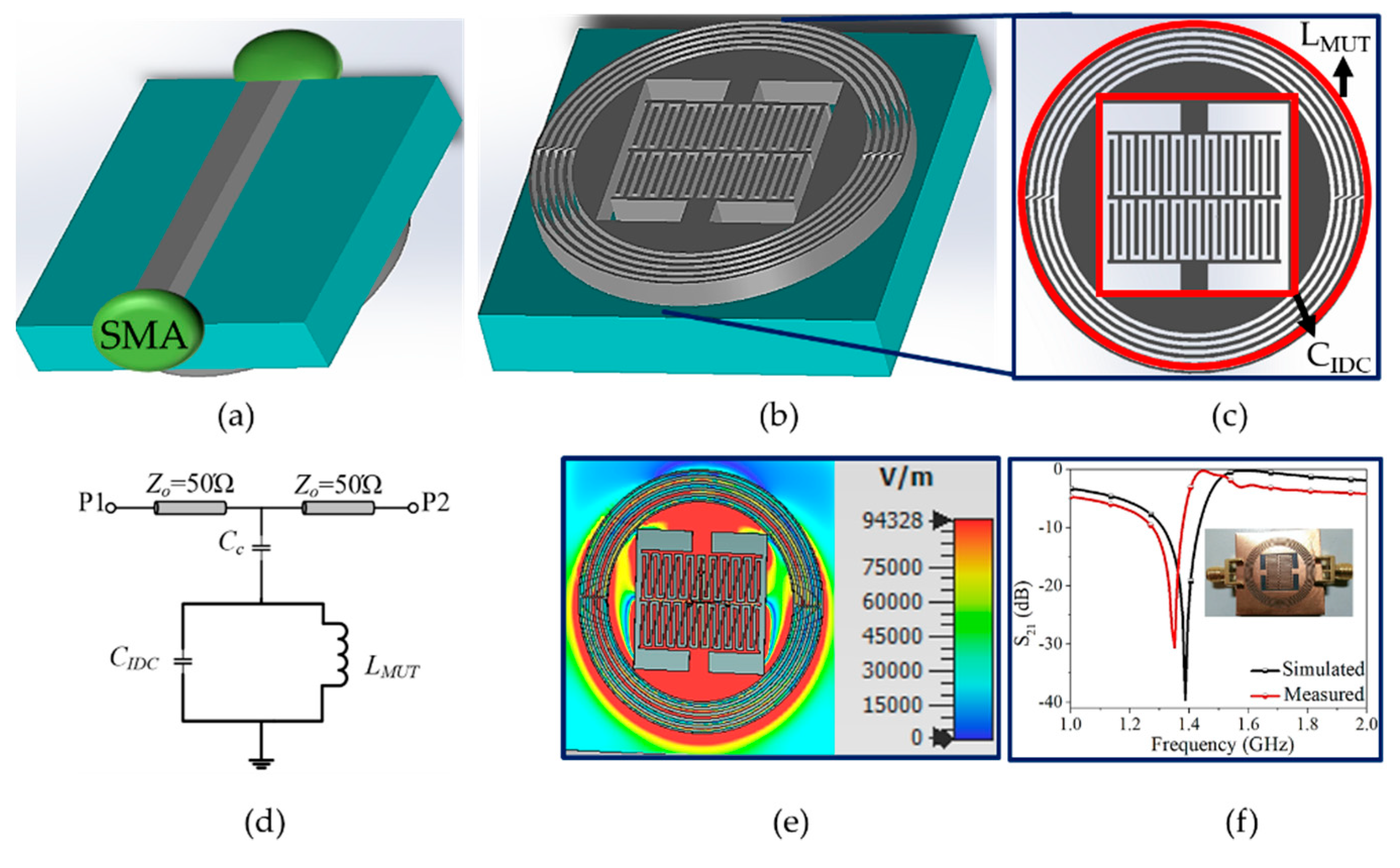
2. Microwave Sensor Design and Operating Principle

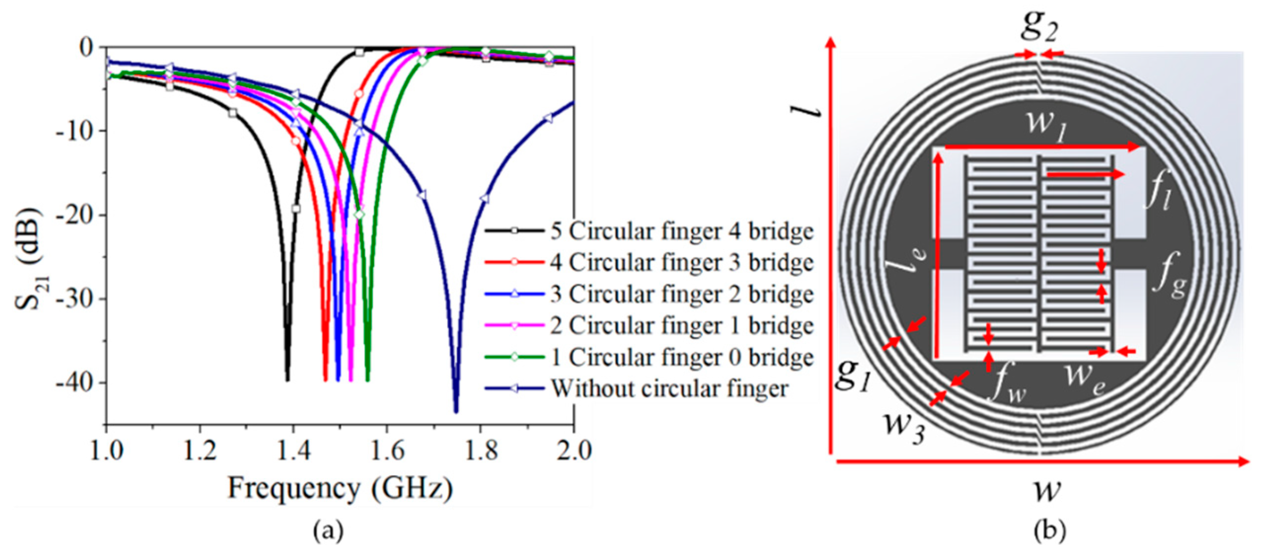
2.1. Microwave Sensor Design

The proposed microwave sensor for measuring materials’ dielectric and thickness properties is designed using a parallel interdigital structure and the symmetrical differential bridge-type inductor. The fingers strip with its gap of the parallel combination of the interdigital structure is employed to achieve a high e-field zone. A differential bridge-type inductor is used to attain high mutual inductance. The designed sensor’s 3D geometry is shown in Figure 1, and the equivalent circuit with its field distribution at 1.38 GHz (see Figure 1f) resonance frequency is depicted in Figure 1d, e, respectively. The proposed microwave sensor resonating frequency ( f r ) depends on the capacitance and inductance of the design, and can be defined as [28]:
f r = 1 2 π L M U T ( C I D C + C C )
The resonance frequency of the proposed microwave sensor is affected by the capacitance and inductance value, as illustrated in Equation (1). The designed sensor circuit model defines that the alteration in coupling capacitance (CC) and parallel IDC structure (CIDC) affect the resonating frequency; thus, it is possible to employ it as an indicator. The total capacitance produced by the combination of CIDC and CC can be approximated as [29]:
C I D C = [ ε ( 1 + ε s 2 ) K ( 1 k 2 ) K ( k ) + ε o f W f g ] l e ( N E 1 )
C c = ε ο ε s 4 K ( k ) K ( k )
In Equations (2) and (3), K(k) defines an elliptical integer of the first kind, ε s is the permittivity of RF-35 substrate, and ε o indicates the permittivity in free space. The le is the length of the electrode, NE represents the number of fingers, and fW and fg define the finger width and gap, respectively. The analysis of interdigital capacitor type structure is essentially based on the sensing zone. The interdigital capacitor is performed like a traditional plate capacitor, but the main benefit lies between adjacent finger strips. The gaps between the fingers of such type of structure are enhancing the total e-field of the resonator. The fingers of interdigital structure and its gaps provide a high electrical potential at the surface of the designed sensor. Once the testing MUTs are loaded on the high field zone, it distracts the entire field, which indicates a variation in the resonance frequency and Q-factor.
The structure analysis of the designed sensor is essential based on fingers and electrodes of the interdigital design. The fingers and electrodes of the IDC structure provide a periodic electric potential at the surface after perturbing the testing sample on the high field zone, as shown in Figure 2. The operating principle of the IDC structure is the same as a capacitor, but the open area between the electrodes and fingers creates a high-intensity field zone suitable for measuring pure dielectric samples. The parallel combination of the interdigital structure provides a high e-field zone, which detects the proximity of testing MUTs even with a minute gap through reflection. Adjusting the gap between the fingers and electrodes indicates a higher interaction between the testing sample and the field [22,30].
Similarly, the inductor is another parameter that also affects the resonating frequency of the proposed microwave sensor. The dual wide gap slit on both sides of the IDC structure is connected with spiral inductance, and the rings are added to enhance the confinement of the e-field. The total inductance produced by the designed sensor is a combination of mutual and self-inductance and can be represented as [31]:
L = 2 L M S ( ln 2 L M S W E F F + H M S 0.5 )
W E F F = = W 0 n ( 1 e ( w w 0 n ) )
W o i = c 1 × c 2 n 1 1 f
In Equations (4)–(6), WEFF determines the effective line width, LMS represents the length of the metal (copper) segment, HMS denotes the height of the metal segment. Similarly, n indicates the number of turns in the coil inductor, C1 and C2 are demonstrated the linearized parameters for the inductance and resistance, respectively. The mutual inductance of the designed sensor mainly depends on the gap between segments and can be defined as [31]:
± L M U T = 2 × 10 4 L M S ( ln ( L M S g + 1 + L M S 2 g 2 ) 1 + L M S 2 g 2 + g L M S )
The proposed design inductor and capacitor value are optimized to attain a lower resonating frequency. The developed sensor interdigital structure generates a high e-field for measuring the sample’s thickness and dielectric properties more accurately with an air gap of 0.3 mm. The different bridge-type inductor is introduced to attain high inductance and lower tunable resonating frequency. The inductance increases with each circular ring included in the bridge structure, and the resonating frequency of the proposed microwave sensor decreases, as shown in Figure 3a. In the CST software, the minimum and maximum values of the different parameters are considered, and the setup solver provides the optimized values of the designed sensor structure. Various parameters of the proposed microwave sensor are optimized (see Figure 3b), as shown in Table 1 (all unit values are mm).

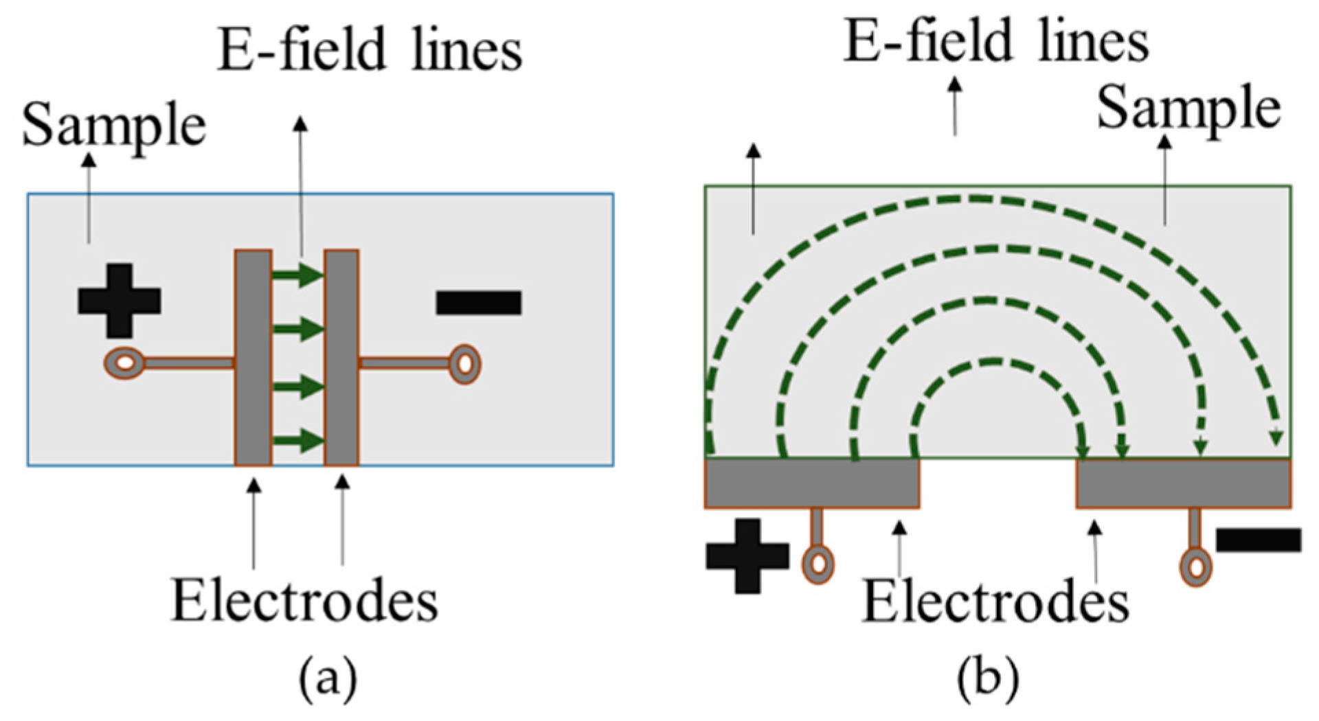
2.2. Operating Principle of the Design

The sensing mechanism of the designed sensor is classified into two categories based on an alteration in the resonance frequency and Q-factor after loading the MUT on the resonator and introducing the air gap scenario between MUT and resonator. The polypropylene strips with various thicknesses represent the gap between the testing MUTs and the resonator. The variation in the resonance frequency and Q-factor of the designed sensor is due to loading an MUT. It was affected due to the permittivity of MUT and interrupted e-field. The designed microwave sensing can be defined from the perturbation theory as given below [1]:
Δ f r f r = v s ( Δ μ H 1 H 0 + Δ ε E 1 E 0 ) d v v s ( μ 0 | H 0 | 2 + ε 0 | E 0 | 2 ) d v
Δ Q r Q r = v s ( Δ μ H 1 H 0 + Δ ε E 1 E 0 ) d v v s ( μ 0 | H 0 | 2 + ε 0 | E 0 | 2 ) d v
In Equations (8) and (9), E0 and H0 represent the e-field and m-field of the unloaded sample, E1 and H1 define the field distribution after loading an MUT on the resonator, and μ 0 and ε 0 represent the permeability and permittivity in free space. The designed sensor is decorated only to characterize the dielectric properties of materials; thus, the terms related to material permeability are neglected. All the tested samples are pure dielectric, and the modified equations can be expressed as [1]:
Δ f r f r = v S ( Δ ε E 1 E 0 ) d v v s ( ε 0 | E 0 | 2 ) d v                        
Δ Q r Q r = v S ( Δ ε E 1 E 0 ) d v v s ( ε 0 | E 0 | 2 ) d v  
In Equations (10) and (11), Δ ε and Δ μ define the permittivity and permeability of a loading MUT on the resonator and v s is represents the volume of a sensing zone. It reveals that once the sample is loaded on the resonator, it variates the resonance frequency and Q-factor of the designed sensor. It is due to the permittivity, volume, and interrupted e-field of a sample, signified through a variation in Q-factor and resonating frequency. The high resolution of the designed sensor reveals that the sample’s position and size are considered accurate.
The proposed microwave sensor detects the complex permittivity and thickness with a gap of 0.3 mm between the resonator and testing MUTs. An air gap scenario is considered an extra layer with an unknown thickness and free space permittivity after loading the MUT on the resonator, as shown in Figure 4b. The alteration in the permittivity and thickness of a testing sample is associated with the resonance frequencies; the air gap between the testing MUT and sample influences the measured result. The polypropylene strip is used for the gap between testing MUTs and resonators, as shown in Figure 4a. The final mapping of the air gap situation between the resonator and testing sample is shown in Figure 4b.
Figure 4b represents the different heights (h1, h2, h3), where h1 is the substrate thickness, h2 denotes the air gap thickness, and the sample thickness is represented by h3. According to the definition of the capacitor, C = ε A / d = ε ( 2 h . ) / ( 2 i 0 ) , the variable 2i0 defines the d, and 2h represents the variable A in the capacitance expression, as shown in Figure 4b. The total capacitance of an MUT with an air gap on the proposed design can be represented as follows [27]:
C MUT   with   air   gap   = ε o ( h 2 ) 2 i 0 + ε 1 ( h 3 h 2 ) 2 i 0 + ε o ( h 0 h 3 ) 2 i 0

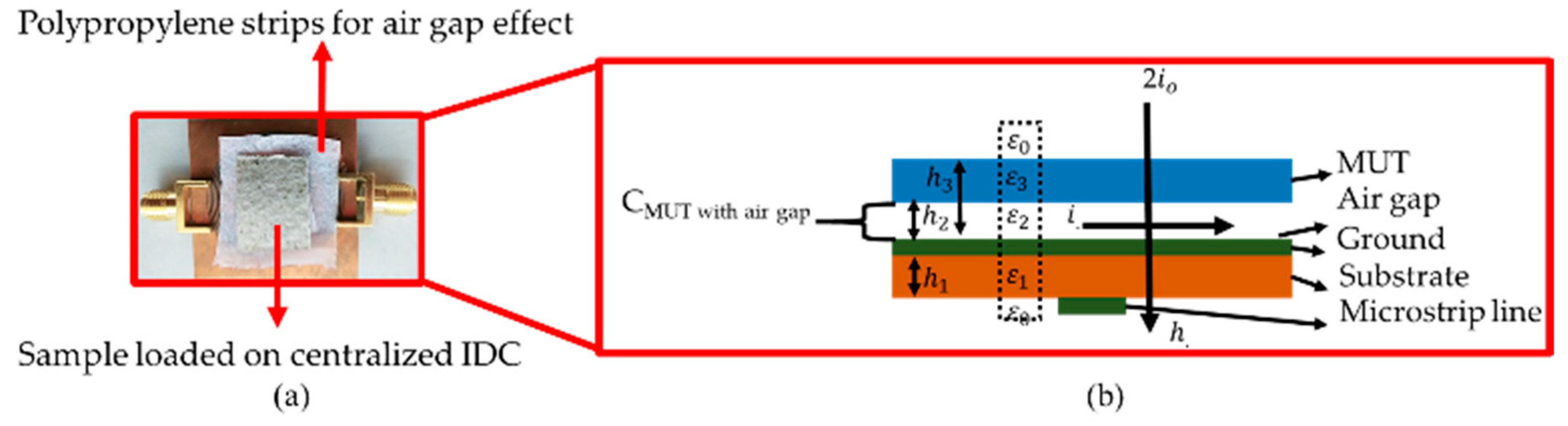
3. Fabrication of the Proposed Design

The proposed microwave sensor is fabricated by using the photolithographic process, as shown in Figure 5. First, a substrate (RF-35) with a height of 0.76 mm and coated with a copper layer of 35 μm thickness on both sides is taken, as shown in Figure 5a. The film’s backside contains the circular fingers inductor and interdigital structure covered with the negative photoresist uniformly. The film is passed through the heated feed rollers for removing vacuum, as shown in Figure 5b. The designed sensor mask is generated by transferring the circular fingers inductor and interdigital structure decoration onto a photographic film with the backing of a photoresist. The prepared cover is examined sensibly without any flaw and placed on the substrate, as shown in Figure 5c. The film with the mask is prebaked in a hotplate at 120 °C for 120 min. This is just for densification of the photoresist layer through evaporating the coating solvent in a hotplate. The entire design is exposed to ultra-violet (UV) light to convey the pattern, as shown in Figure 5c. Finally, with the help of an etchant solution, the unwanted copper is removed gradually, and the photoresist layer is also appropriately removed via acetone. The proposed design is excited by using the SMA connectors at the input and output ports of the microstrip line, as shown in Figure 5d. The designed microwave sensor’s good conductivity and reliability can be verified during the measurement process by encapsulating both connectors with UV light. In the designed microwave sensor, the microstrip line is utilized to attain a 50-ohm characteristic matching impedance.

4. Experimental Results and Discussion

The proposed microwave sensor operates at 1.38 GHz resonance frequency and precisely measures pure dielectric material’s thickness and complex permittivity. The designed sensor is decorated with a centralized IDC structure to generate a high e-field zone and differential bridge-type inductance for a lower tunable resonating frequency, as shown in Figure 6a–l. Each circular finger of the designed sensor illustrates that the total inductance increases and the resonant frequency of the proposed microwave sensor decreases, as shown in Figure 3a. The developed sensor analyzed the thickness and complex permittivity of a sample, which is explained below.

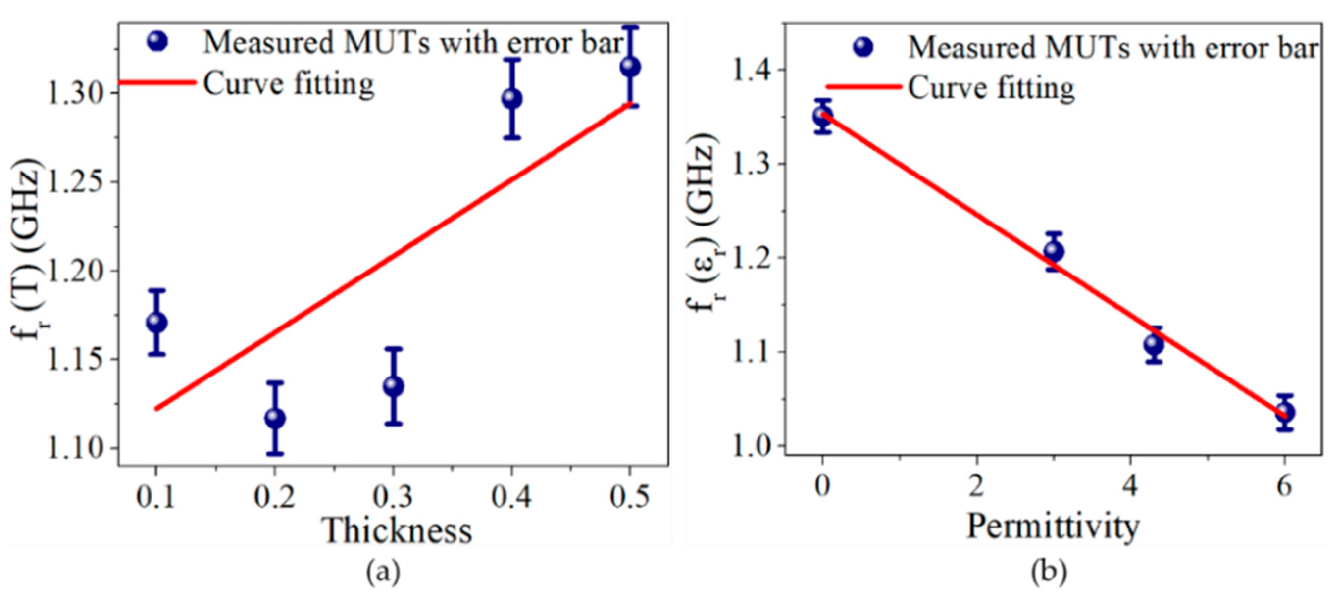
4.1. Analysis of Complex Permittivity with Air Gap Scenario

The measurement analysis of the proposed design is based on the dielectric constant and dielectric loss tangent of the MUTs, loaded on the centralized IDC structure. The thickness of each sample remains constant during the measurement analysis of complex permittivity. This is because under specific thickness, the field interaction of the resonator with the sample saturates, and the alteration in the sensor response is not considered. Once the permittivity of MUTs such as rogers RO3003 ( ε r = 3 and tanδ = 0.001 ), FR4 ( ε r = 4.3 and tanδ = 0.025 ), and mica ( ε r = 6 ) are loaded on the high e-field distribution zone of the centralized IDC structure, the resonance frequency of the designed sensor changes. Such changes in the resonance frequency of the resonator determine the relative permittivity of MUTs. The real and imaginary permittivity of all the testing samples can be calculated from the following expression:
ε r = ε r j ε r
A curve fitting technique is employed to investigate the relationship between shifting in the resonance frequency and loaded MUTs permittivity, as expressed in Equation (14).
ε r = 80.53217 Δ f r 2 3.33755 Δ f r + 0.04647
In Equation (14), Δfr represents the alteration of the resonance frequency with different MUTs loaded on the resonator. The polypropylene strips are introduced between the testing MUT and resonator with varying thicknesses from 0.01–0.3 mm, as shown in Figure 7a–f. The designed sensor sensing accuracy is 97% for estimating the relative part of the permittivity with an excellent correlation coefficient (r2 = 0.97765). The dielectric loss tangent of each testing MUTs is calculated from Equation (15).
tan δ = ε r / ε r
The Q-factor of the proposed design can be influenced by the dielectric loss tangent and relative permittivity of the testing MUTs. The Q-factor of the proposed design for the unloaded sample can be calculated from the following expression (Equation (16))
Q = f r Δ f r ( f u p p e r f l o w e r )
The intercept point between all the testing MUTs can be calculated using the curve fitting technique between the inverse Q-factor and dielectric loss tangent of the loaded MUTs, as expressed in Equation (17).
Q 1 = Slope ( tan δ ) + 0.00744 )
The slope expression is generated from several sets of expressions. It is due to the different relative permittivity of the MUTs loading on the centralized IDC structure. The curve fitting is implemented again between the different slopes expression and relative permittivity of the testing MUTs, as illustrated in Equation (18).
Slope = 0.00575 ( ε r ) 0.00278
tan δ = | Q 1 0.00744 | 0.00575 ( ε r ) 0.00278
Finally, the dielectric loss tangent of all testing MUTs is verified from Equation (19). The designed sensor’s sensing accuracy is 92% for estimating the dielectric loss tangent of the testing specimen with an excellent correlation coefficient (r2 = 0.92694).
Similarly, the frequency detection resolution (FDR) of the designed sensor is 7.2 MHz/Δ ε r . FDR is the measurement analysis of the sensitivity for each change in the permittivity of a testing MUT. The developed sensor’s normalized sensitivity (S%) is 0.51% for measuring the high permittivity MUT with an air gap of 0.3 mm. The performance of the designed sensor is compared with several previous reported works based on the air gap scenario, normalized sensitivity, and FDR, as expressed in Table 2. The difference between the measured |S21| and simulation of the proposed microwave sensor is low, and it exhibits a small error ratio for measuring all the testing MUTs. The performance of the designed sensor based on the error ratio is represented in Table 3.

4.2. Analysis of Thickness with Air Gap Scenario

The proposed microwave sensor also investigated the effect of thickness variation with an air gap, as shown in Figure 8a–c. Mica is selected as a testing MUT with a constant dielectric constant for accurate analysis of the thickness effect on the designed sensor’s resonance frequency. Mica has a wide variety of thicknesses ranging from 0.1–0.5 mm, as shown in Figure 8a. The previous mechanism is implemented to analyze the thickness parameter; all the testing samples are loaded on the centralized IDC structure with high e-field distribution. The resonance frequency of the designed sensor changes by perturbing the mica sample with the varying thickness in the high e-field zone.
MATLAB programming is used to find the polynomial interpolation for evaluating the relationship between resonance frequency (fr) and frequency shifting (Δfr) against the variation in the gap between the designed sensor and mica thicknesses. The polynomial interpolation between the measured resonance frequency and frequency shifting of mica MUTs against the various gap variations is shown in Figure 8b,c, which can be defined as:
f r ( t m ) = 1.965 t m 4 385.87536 t m 3 + 8587.50688 t m 2 47 , 812.53646 t m + 1.171
Δ f r ( t m ) = 7.2 t m 4 + 56.1 t m 3 162 t m 2 + 150 t m + 0.522
Equation (20) defines that if the tested variable is the resonating frequency, then the polynomial interpolation between the measured sample with a varying air gap can be graphically depicted in Figure 8b. Similarly, Equation (21) exhibits the relationship between the total variation in the resonance frequency and mica thickness after loading it on the designed sensor with varying air gaps, as explained in Figure 8c.
The variables such as resonance frequency and frequency shifting are known variables; the thickness of the sample is the unknown variable. The thickness of each MUT can be numerically estimated by taking a polynomial interpolation between the tested frequency shifting and unknown variables as given below:
t m = 90.74796 Δ f r 4 1115.23079 Δ f r 3 + 5129.18723 Δ f r 2 7903.95738 Δ f r 1.95455
The proposed microwave sensor determined the thickness and complex permittivity of a material with a varying gap between the testing MUT and resonator simultaneously. The comparison of the designed sensor with the previously reported work based on different performance characteristics is illustrated in Table 4.
A Keysight microwave analyzer (N9916A) is used to ensure the S-parameter of the proposed microwave sensor. The Keysight was attuned before using a short, open, load, and throughput (SOLT) method to provide the best measurement accuracy. The measurement setup was conducted at room temperature (21.1 °C ± 0.02%) and humidity (49.5 ± 0.03%), as expressed in Figure 9. The measurement results of all the loaded samples are determined through a variation in the transmission coefficient (|S21|). The frequency range is set to 1–2 GHz for the measurement setup, and the polypropylene strips are used for an air gap effect, as shown in Figure 9.
The linear regression analysis was performed between the loaded sample (permittivity and thickness MUTs) and measured resonating frequency, prepared to calibrate the sensor. The designed sensor indicated a linear response with a good correlation coefficient (r2 = 0.91567 for thickness and r2 = 0.98903 for permittivity MUTs). It can be defined using the following regression equations (Equations (23) and (24)) for thickness and permittivity of the samples, as shown in Figure 10a,b.
f r ( T ) = 0.0415674 α m m + 1.16344
f r ( ε r ) = 0.05352 α ε r + 1.35313
In Equations (23) and (24), αmm represents the thickness of the mica sample and α ε r denotes the permittivity of loaded MUTs. Therefore, the fr of the designed sensor revealed high sensitivities (41 MHz/mm for thickness and 53 MHz/Δ ε r for permittivity sample) towards the measurement of thickness and permittivity of the specimen, simultaneously via a single sensor. The resolution and reproducibility of the proposed design are evaluated using a triplicate analysis of each sample. The designed sensor reveals a minute variation in the sample measurement, and it is estimated using the triplicate measurement analysis for permittivity (0.05734) and thickness (0.04618) of the samples. The high reproducibility is predictable, and it is due to the usage of a microwave analyzer (N9916A), which is calculated more precisely by the variation in the resonance frequency (down to 5 kHz). The linearity operation for the MUTs thickness concerning various gap variations is little degraded, as shown in Figure 10a. This is because the resonance frequency of the designed sensor is influenced by the MUTs thickness and different strips variations. The proposed sensor’s correlation coefficient for measuring the mica thickness linear response is r2 = 0.91567. This effect can be minimized by decreasing the gap between the MUTs thickness and resonator. It depends on the measurement setup, and users can utilize it according to their terms and conditions.

5. Conclusions

In this article, a non-contact optimized microwave sensor is designed and fabricated to measure pure dielectric material’s thickness and complex permittivity with varying air gaps. The developed sensor is based on the differential bridge-type inductor (for high Q-factor and lower tunable resonating frequency) and centralized IDC structure for the generation of high e-field zone to measure the thickness and dielectric properties of a material more accurately. The designed sensor’s different parameters are optimized for the configuration of the spur-line structure to produce a high-intensity e-field at the loaded centralized IDC zone. The high sensitivity of the designed sensor is realized in the FDR (7.2 MHz/Δ ε r ) and fr (53 MHz/Δ ε r and 41 MHz/mm) for measuring the thickness and complex permittivity of MUTs with varying air gaps of 0.1 mm and 0.3 mm, respectively. The proposed microwave sensor exhibits an excellent sensing accuracy of 97% and 92% for the real and imaginary parts of the permittivity, respectively. Moreover, the curve fitting technique between the testing sample with varying thickness, permittivity, and air gap exhibited an excellent accuracy, authenticating its application in the non-contact measurement of material. The designed sensor performance affirms its application in the non-contact measurement of complex permittivity and thickness of different pure dielectric MUTs simultaneously.

Author Contributions

Conceptualization, L.A.; methodology, L.A.; software, L.A., validation, L.A., C.W. and I.U.; formal analysis, L.A., R.K., S.U., F.A. and H.H.; investigation, L.A.; resources, C.W., I.U. and W.U.K.; data curation, R.K., A.Y., S.U., F.A. and M.S.; writing—original draft preparation, L.A.; writing—review and editing, L.A., M.S. and C.W.; visualization, C.W. and S.U.; supervision, C.W. and I.U; project administration, C.W., I.U. and M.S.; funding acquisition, H.H. All authors have read and agreed to the published version of the manuscript.

Funding

This Work was supported by Taif University Researchers Supporting Project (TURSP), Taif University, Kingdom of Saudi Arabia under the grant number: TURSP-2020/150.

Data Availability Statement

The dataset used for the experiments in this study is available upon reasonable request from the corresponding author.

Acknowledgments

We deeply acknowledge Taif University for supporting this study through Taif University Researchers Supporting Project Number (TURSP-2020/150), Taif University, Taif, Saudi Arabia. This work was also supported by the General Financial Grant from the China Postdoctoral Science Foundation (2017M611367), Heilongjiang Postdoctoral Science Foundation (LBH-Z17056), NSF of China (No. 61971160), Development Program of China (2019YFE0121800), and Zhejiang Lab (2019MC0AB03).

Conflicts of Interest

The authors declare no conflict of interest.

References

  1. Safa, M.S.; Nayyeri, V.; Khanjarian, M.; Soleimani, M.; Ramahi, O.M. A CSRR-based sensor for full characterization of magneto-dielectric materials. IEEE Trans. Microw. Theory Tech. 2019, 67, 806–814. [Google Scholar] [CrossRef]
  2. Shi, P.; Gao, R.; Liu, S.; Yuan, Y. Topology optimization-based design of metamaterial-inspired sensor with improved sensitivity. Sens. Act. A Phys. 2017, 268, 83–90. [Google Scholar] [CrossRef]
  3. Subbaraj, S.; Ramalingam, V.S.; Kanagasabai, M.; Sundarsingh, E.F.; Selvam, Y.P.; Kingsley, S. Electromagnetic nondestructive material characterization of dielectrics using EBG based planar transmission Line sensor. IEEE Sens. J. 2016, 16, 7081–7087. [Google Scholar] [CrossRef]
  4. Kiani, S.; Rezaei, P.; Navaei, M.; Abrishamian, M.S. Microwave sensor for detection of solid material permittivity in single/multi-layer samples with high-quality factor. IEEE Sens. J. 2018, 18, 9971–9977. [Google Scholar] [CrossRef]
  5. Rusni, I.M.; Ismail, A.; Alhawari, A.R.H.; Hamidon, M.N.; Yusof, N.A. An aligned-gap and centered-gap rectangular multiple split-ring resonator for dielectric sensing applications. Sensors 2014, 14, 13134–13148. [Google Scholar] [CrossRef] [PubMed]
  6. Li, Y.; Bowler, N.; Jhonson, D.B. A resonant microwave patch sensor for detection of layer thickness or permittivity variations in multilayered dielectric structures. IEEE Sens. J. 2011, 11, 5–15. [Google Scholar] [CrossRef]
  7. Rahman, M.N.; Islam, M.T.; Samsuzzaman, S.M. Resonator based metamaterial sensor to detect unknown materials. Microw. Optical Technol. Lett. 2018, 60, 1681–1685. [Google Scholar] [CrossRef]
  8. Romera, G.G.; Martinez, F.J.H.; Gil, M.; Martinez, J.J.M.; Vargas, D.S. Submersible printed split-ring resonator-based sensor for thin-film detection and permittivity characterization. IEEE Sens. J. 2016, 16, 3587–3596. [Google Scholar] [CrossRef]
  9. Karami, M.; Rezaei, P.; Kiani, S.; Sadeghzadeh, R.A. Modified planar sensor for measuring dielectric constant of liquid materials. Electron. Lett. 2017, 53, 1300–1302. [Google Scholar] [CrossRef]
  10. Jankovic, N.; Radonic, V. A microwave microfluidic sensor based on a dual-mode resonator for dual-sensing applications. Sensors 2017, 17, 2713. [Google Scholar] [CrossRef] [Green Version]
  11. Benkhaoua, L.; Benhabiles, M.T.; Mouissat, S.; Riabi, M.L. Miniaturized quasi-lumped resonator for dielectric characterization of liquid mixtures. IEEE Sens. J. 2016, 16, 1603–1610. [Google Scholar] [CrossRef]
  12. Horestani, A.K.; Naqui, J.; Abbott, D.; Fumeaux, C.; Martin, F. Two dimensional displacement and alignment sensor based on reflection coefficients of open microstrip lines loaded with split-ring resonators. Electron. Lett. 2014, 50, 620–622. [Google Scholar] [CrossRef] [Green Version]
  13. Ebrahimi, A.; Withayachumnankul, W.; Sarawi, S.A.; Abbott, D. High-sensitivity metamaterial-inspired sensor for microfluidic dielectric characterization. IEEE Sens. J. 2014, 14, 1345–1351. [Google Scholar] [CrossRef] [Green Version]
  14. Mckeown, M.S.; Julrat, S.; Trabelsi, S.; Tollner, E.W. Open transverse slot substrate integrated waveguide sensor for biomass permittivity determination. IEEE Trans. Instrum. Meas. 2017, 66, 2181–2188. [Google Scholar] [CrossRef]
  15. Saghati, A.P.; Batra, J.S.; Kameoka, J.; Entesari, K. A meta-material inspired wideband microwave interferometry sensor for dielectric spectroscopy of liquid chemicals. IEEE Trans. Microw. Theory Tech. 2017, 65, 2558–2571. [Google Scholar] [CrossRef]
  16. Shafi, K.T.M.; Jha, A.K.; Akhtar, M.J. Improved planar resonant RF sensor for retrieval of permittivity and permeability of materials. IEEE Sens. J. 2017, 17, 5479–5486. [Google Scholar] [CrossRef]
  17. Yeo, J.; Lee, J.L. High sensitivity microwave sensor based on an interdigital capacitor shaped defected ground structure for permittivity characterization. Sensors 2019, 19, 498. [Google Scholar] [CrossRef] [Green Version]
  18. Alahnomi, R.A.; Zakaria, Z.; Ruslan, E.; Rashid, S.R.A.; Bahar, A.A.M. High-Q sensor based on symmetrical split ring resonator with spurlines for solids material detection. IEEE Sens. J. 2017, 17, 2766–2775. [Google Scholar] [CrossRef]
  19. Lee, H.J.; Lee, J.H.; Moon, H.S.; Jang, I.S.; Choi, J.S.; Yook, J.G.; Jung, H.L. A planar split-ring resonator-based microwave biosensor for label-free detection of biomolecules. Sens. Act. B Chem. 2012, 169, 26–31. [Google Scholar] [CrossRef]
  20. Velez, P.; Su, L.; Grenier, K.; Contreras, J.M.; Dubuc, D.; Martin, F. Microwave microfluidic sensor based on a microstrip splitter/combiner configuration and split ring resonators (SRRs) for dielectric characterization of liquids. IEEE Sens. J. 2017, 17, 6589–6598. [Google Scholar] [CrossRef] [Green Version]
  21. Ebrahimi, A.; Scott, J.; Ghorbani, K. Ultrahigh sensitivity microwave sensor for microfluidic complex permittivity measurement. IEEE Trans. Microw. Theory Tech. 2019, 67, 4269–4277. [Google Scholar] [CrossRef]
  22. Mamishev, A.V.; Du, Y.; Lesieutre, B.C.; Zahn, M. Development and applications of fringing electric field dielectrometry sensors and parameter estimation algorithms. J. Electrostat. 1999, 46, 109–123. [Google Scholar] [CrossRef]
  23. Rahman, M.S.A.; Mukhopadhyay, S.C.; Yu, P.L. Novel planar interdigital sensors. Smart Sens. Meas. Instrum. 2014, 10, 11–35. [Google Scholar]
  24. Bonache, J.; Gil, M.; Gil, I.; Garcia, J.; Martin, F. On the electrical characteristics of complementary metamaterial resonators. IEEE Micro. Wirel. Comp. Lett. 2006, 16, 543–545. [Google Scholar] [CrossRef]
  25. Sun, H.R.; Du, G.; Liu, G.; Sun, X.; Tang, T.; Liu, W.; Li, R. Symmetric coplanar waveguide sensor loaded with interdigital capacitor for permittivity characterization. Int. J. RF Microw. Comput. Eng. 2020, 30, e22023. [Google Scholar] [CrossRef]
  26. Kapoor, A.; Varshney, P.K.; Akhtar, M.J. Interdigital Capacitor Loaded Electric-LC Resonator for Dielectric Characterization. Microw. Opt. Technol. Lett. 2020, 62, 2835–2840. [Google Scholar] [CrossRef]
  27. Yang, C.L.; Lee, C.S.; Chen, K.W.; Chen, K.Z. Non-contact measurement of complex permittivity and thickness by using planar resonators. IEEE Trans. Microw. Theory Tech. 2016, 64, 247–257. [Google Scholar] [CrossRef]
  28. Wang, C.; Ali, L.; Meng, F.; Adhikari, K.K.; Zhou, Z.L.; Wei, Y.; Zou, D.Q.; Yu, H. High accuracy complex permittivity characterization of solid materials using parallel interdigital capacitor-based planar microwave sensor. IEEE Sens. J. 2020, 21, 6083–6093. [Google Scholar] [CrossRef]
  29. Keat, G.O.; Craig, A.G. A resonant printed-circuit sensor for remote query monitoring of environmental parameters. Smart Mater. Struct. 2000, 9, 421–428. [Google Scholar]
  30. Nurage, N.; Su, K. Perovskite ferroelectric nanomaterials. Nanoscale 2013, 5, 8752–8780. [Google Scholar] [CrossRef] [PubMed]
  31. Chen, J. On-Chip Spiral Inductor Transformer Design and Modeling for RF Applications. Ph.D. Thesis, University of Central Florida, Orlando, FL, USA, 2006. [Google Scholar]
  32. Ebrahimi, A.; Scott, J.; Ghorbani, K. Transmission lines terminated with LC resonators for differential permittivity sensing. IEEE Microw. Wirel. Compon. Lett. 2018, 28, 1149–1151. [Google Scholar] [CrossRef]
  33. Ali, L.; Wang, C.; Meng, F.; Adhikari, K.K.; Wei, Y.; Li, J.H.; Song, Z.W.; Zhao, M. Design and optimization of interdigitated microwave sensor for multidimensional sensitive characterization of solid materials. IEEE Sens. J. 2021, 21, 22814–22822. [Google Scholar] [CrossRef]
  34. Su, L.; Contreras, J.M.; Velez, P.; Martin, F. Configurations of splitter/combiner microstrip sections loaded with stepped impedance resonators (SIRs) for sensing applications. Sensors 2016, 16, 2195. [Google Scholar] [CrossRef] [Green Version]
  35. Ebrahimi, A.; Beziuk, G.; Scott, J.; Ghorbani, K. Microwave differential frequency splitting sensor using magnetic-LC resonators. Sensors 2020, 20, 1066. [Google Scholar] [CrossRef] [PubMed] [Green Version]
  36. Ali, L.; Wang, C.; Meng, F.; Wei, Y.; Tan, X.; Adhikari, K.K.; Zhao, M. Simultaneous measurement of thickness and permittivity using microwave resonator-based planar sensor. Int. J. RF Microw. Comput. Eng. 2021, 31, e22794. [Google Scholar] [CrossRef]
Figure 1. The 3D geometry of the proposed non-contact optimized microwave sensor layout: (a) front side of the proposed design; (b) backside of the proposed design; (c) simulation-based bridge-type structure; (d) equivalent circuit of the designed sensor; (e) strength of high intensity coupled e-field revealing a maximum field at the center of the developed sensor; and (f) comparison of the resonating frequency of simulated and measured prototype for unloaded MUTs.
Electronics 10 03057 g001
Figure 2. (a) Traditional plate capacitor e-field lines and (b) IDC structure capacitor e-field lines.
Electronics 10 03057 g002
Figure 3. (a) Lower tunable resonating frequency of optimized microwave sensor and (b) different parameters of the developed sensor.
Electronics 10 03057 g003
Figure 4. (a) Designed sensor under testing with polypropylene strip between the testing specimen and resonator and (b) dimension of the mapping air gap scenario between MUT and resonator.
Electronics 10 03057 g004
Figure 5. Fabrication steps of the proposed prototype: (a) RF-35 substrate with copper decoration on both sides; (b) photoresist layer on the backside of the film; (c) patterned mask on the film with UV light exposure for moving design on the substrate; (d) the proposed microwave sensor with SMA connectors.
Electronics 10 03057 g005
Figure 6. Proposed microwave sensor with e-field distribution at the lower tunable resonant frequency; (a) designed sensor without a circular finger; (b) with one circular finger; (c) with two circular fingers and one bridge-type structure; (d) with three circular fingers and two bridge-type structure; (e) with four circular fingers and three bridge-type structure; (f) with five circular fingers and four bridge-type structure; (g) e-field at 1.74 GHz; (h) 1.55 GHz; (i) 1.52 GHz; (j) 1.49 GHz; (k) 1.46 GHz; and (l) 1.38 GHz.
Electronics 10 03057 g006
Figure 7. |S21|measured analysis of different permittivity MUTs loaded on the high e-field centralized IDC structure with varying air gaps ranging from 0.01–0.3 mm; (a) FR4 MUT; (b) rogers RO3003 (Rog) MUT; (c) mica MUT curve fitting technique analysis with error bars for the triplicate measurement of testing MUTs with varying air gap scenario; (d) FR4; (e) rogers RO3003; and (f) mica.
Electronics 10 03057 g007
Figure 8. (a) |S21|measured analysis of different thicknesses of mica MUT loaded on the high e-field centralized IDC structure with varying air gaps; (b) resonance frequency; and (c) frequency shifting (note: Equations (20) and (21) based on Figure 8b,c were arbitrarily proposed).
Electronics 10 03057 g008
Figure 9. Measurement setup of the proposed design: (a) designed sensor under testing; (b) back view of the designed sensor; (c) polypropylene strips between designed microwave sensor and MUT; (d) fabricated bridge-type structure.
Electronics 10 03057 g009
Figure 10. (a) Linear regression graph as per change in MUTs thickness with error bar indicating an excellent linear response (r2 = 0.91567); (b) linear regression graph as per change in MUTs permittivity with error bar indicating an excellent linear response (r2 = 0.98903).
Electronics 10 03057 g010
Table 1. Different optimized parameters of the proposed microwave sensor.
ParametersAbbreviationMinimum ValueOptimized ValueMaximum Value
fwFinger width0.10.30.4
fgFinger gap0.20.3250.5
leLength of electrode7.012.514.0
weWidth of electrode0.10.30.5
flFinger length2.04.06.0
w1Gap between electrode6.09.012.0
w3Width of circular finger0.10.310.5
g1Gap between circular finger0.10.310.5
g2Gap between bridge-type structure0.150.30.45
lLength of the proposed design----15
wWidth of the proposed design----15
Table 2. Proposed microwave sensor comparison based on complex permittivity analysis with previously reported literature.
Referencesfr (GHz) ε r   Range S (%)FDR (MHz)Maximum Gap (mm)Sensing Accuracy
[1]2.473.25–6.21.7400--
[3]2.452.09–6.920.5100--
[28]2.352.2–10.53.98290099.9% and 99.7%
[32]2.02.2–10.23.32250--
[33]5.791.6–6.154.3373099% and 97%
[34]3.62.43–10.21.22100--
[35]2.182.2–10.73.592450--
[36]1.82.2–10.53.3963099% and 87%
Proposed design1.383–60.517.20.397% and 92%
Table 3. Measurement analysis of the designed sensor based on error ratio for the different permittivity MUTs.
Sample Reference   ε r Extracted   ε r Reference tanδExtracted tanδError (%)
FR43.0 ± 0.23.05 0.0250.02378493.86
Rogers4.3 ± 0.154.25 0.0010.00156494.49
Mica6.1 ± 0.26.15----6.52
Table 4. Comparison of the designed sensor based on different performance characteristics.
References ε r tanδAir GapThickness
[1]
[2]
[6]
[7]
[33]
[36]
Proposed design
Publisher’s Note: MDPI stays neutral with regard to jurisdictional claims in published maps and institutional affiliations.

