Article

A Robust Multilevel Inverter Topology for Operation under Fault Conditions

1
Department of Electrical Engineering, ZHCET, Aligarh Muslim University, Aligarh 202002, Uttar Pradesh, India
2
Industrial Engineering Department, College of Engineering, King Saud University, P.O. Box 800, Riyadh 11421, Saudi Arabia
3
Faculty of Information Technology, Engineering and Economics, Oestfold University College, 1757 Fredrikstad, Norway
4
Electrical Engineering Department, College of Engineering, King Saud University, P.O. Box 800, Riyadh 11421, Saudi Arabia
*
Authors to whom correspondence should be addressed.
Electronics 2021, 10(24), 3099; https://doi.org/10.3390/electronics10243099
Submission received: 11 November 2021 / Revised: 27 November 2021 / Accepted: 30 November 2021 / Published: 13 December 2021
(This article belongs to the Special Issue Environment and Electrical Engineering-Edition 2021)

Abstract

:
Multilevel inverters (MLIs) are used on a large scale because they have low total harmonic distortion (THD) and low voltage stress across the switches, making them ideal for medium- and high-power applications. The authenticity of semiconductor devices is one of the main concerns for these MLIs to operate properly. Due to the large number of switches in multilevel inverters, the possibility of a fault also arises. Hence, a reliable five-level inverter topology with fault-tolerant ability has been proposed. The proposed topology can withstand an open-circuit (OC) fault caused when any single switch fails. In comparison to typical multilevel inverters, the proposed topology is fault-tolerant and reliable. The simulation of the proposed topology is conducted in MATLAB-Simulink and PLECS software packages, and the results obtained for normal pre-fault, during-fault, and after-fault conditions are discussed. Experimental results also prove the proposed cell topology’s robustness and effectiveness in tolerating OC faults across the switches. Furthermore, a thorough comparison is provided to demonstrate the proposed topology’s superiority compared to recently published topologies with fault-tolerant features.

1. Introduction

An ever-increasing demand for electrical energy has resulted in the severe depletion of traditional energy sources, which has led to large-scale research into a renewable energy source (RES)-based power generation. New power converter technologies are necessary for intended operation, control, and power management in order to increase power quality. Multilevel inverters were first introduced in early 1975 [1]. These MLIs are becoming increasingly popular due to their high voltage operation ability, higher efficiency, lower switching losses, and lesser electromagnetic interference [2]. MLIs are one of the best options to fulfill the increasing demand for power. MLIs can produce staircase-like AC voltage by the unique connections of switches with DC sources [3]. Due to these advantages, MLIs are widely used in place of two-level inverters.
To increase efficiency, the total harmonic distortion (THD) of the inverter must be decreased. The square-wave output contains an infinite number of harmonics, and to reduce this, we must make multilevel level output that is close to the sinusoidal waveform with reduced harmonics in the output voltage. Multilevel inverters can be of the 2n + 1 type, where n is an integer [4]. A multilevel inverter requires more switches, increasing the possibility of switching failure, and therefore, the unbalanced output voltage is obtained, causing increased THD in the output voltage. Inverters, based on the source, are of two types [1]: (1) the current source type and (2) the voltage source inverter. Based on the source type, a multilevel inverter is further classified as (1) a single DC source or (2) a multiple DC source. In a single DC source multilevel inverter, there are two types: the first is asymmetric, meaning the DC sources’ voltage across the terminal is equal, and the second is asymmetrical, meaning the voltage across the terminal is unequal. The above classification of the inverter is provided in Figure 1.
The well-known conventional topologies of the multilevel inverter are used in different industrial applications due to the unique features of these topologies; however, they need a significant number of the fundamental components of MLIs, such as switches, DC power supplies, capacitors, and diodes, as we are moving towards higher voltage levels. A comparison of the fundamental component of conventional topologies is provided in Table 1 [5], where t is the number of levels. Flying capacitors use additional capacitors, which are clamped across the switches to produce extra voltage. The diode-clamped inverter uses a clamp diode along with a capacitor to produce multilevel output voltage. Flying capacitors, and diode-clamped MLIs, have the disadvantage of needing many capacitors and diodes to produce higher levels. In contrast, cascaded H-bridge inverters contain multiple, separate DC sources and many power semiconductor devices for generating higher levels, and external circuits are required to maintain the capacitor voltage. They also create the problem of unbalancing capacitor voltage in addition to the incapability of self-voltage boosting.
MLIs have low reliability, which is the main area of concern, and this low reliability is due to the power switches that are most vulnerable in nature, but in reality, we use more devices due to the above-mentioned advantages, and this opens the possibility for researchers to reduce the device count. Again, there is a problem when using a smaller number of power switches and redundant path reduction for uninterrupted system use because we have to make the system fault-tolerant. Multiple open-circuit faults are a possible scenario. In this paper, we will study what happened after fault operation due to a fault in a single switch of the circuit. MLIs are used in different applications, including machine drives and renewable-energy conversion such as photovoltaic systems, and these applications require an undisturbed, continuous, and protected mode of application. As a result, we require robust and reliable power inverters, which are essential for maintaining the power supply [6]. The literature in [7] looked into post-fault operation and topologies. In terms of fault-tolerant operations, the previous works of literature have presented a variety of methodologies. Several fault operation methods are classified into four categories. The first solution involves redundant operation. In the second solution, the fundamental concept of the leg-level is to provide redundant legs in the parallel or series connections to the main legs, where the redundant parallel leg offers a better combination of system cost and performance. In the third solution, a module of the multilevel inverter is used, such as cascaded-H bridge (CHB) modular multilevel converters (MMCs), for making the circuit fault-tolerant. Lastly, in the fourth solution, redundant series or parallel converters are used to tolerate the fault. Several techniques have been used to extend the lifetime of long-run power devices, including cooling devices [8], power derating [9], and modulation method reconfiguration. However, these approaches fail when the switch is utterly wrecked; in this situation, only topology reconfiguration works.
The remaining paper is laid out as follows. In Section 2, the five-level fault-tolerant topology is proposed. Section 3 presents the conventional NLC applied to the proposed inverter. In Section 4, power loss analysis is performed on the proposed inverter. Section 5 and Section 6 provide the simulation verification and experimental validation of the discussed inverter, respectively. In Section 7, a comparison between similar inverter topologies is presented. Section 8 concludes the paper.

2. Proposed Five-Level Fault-Tolerant MLI Topology

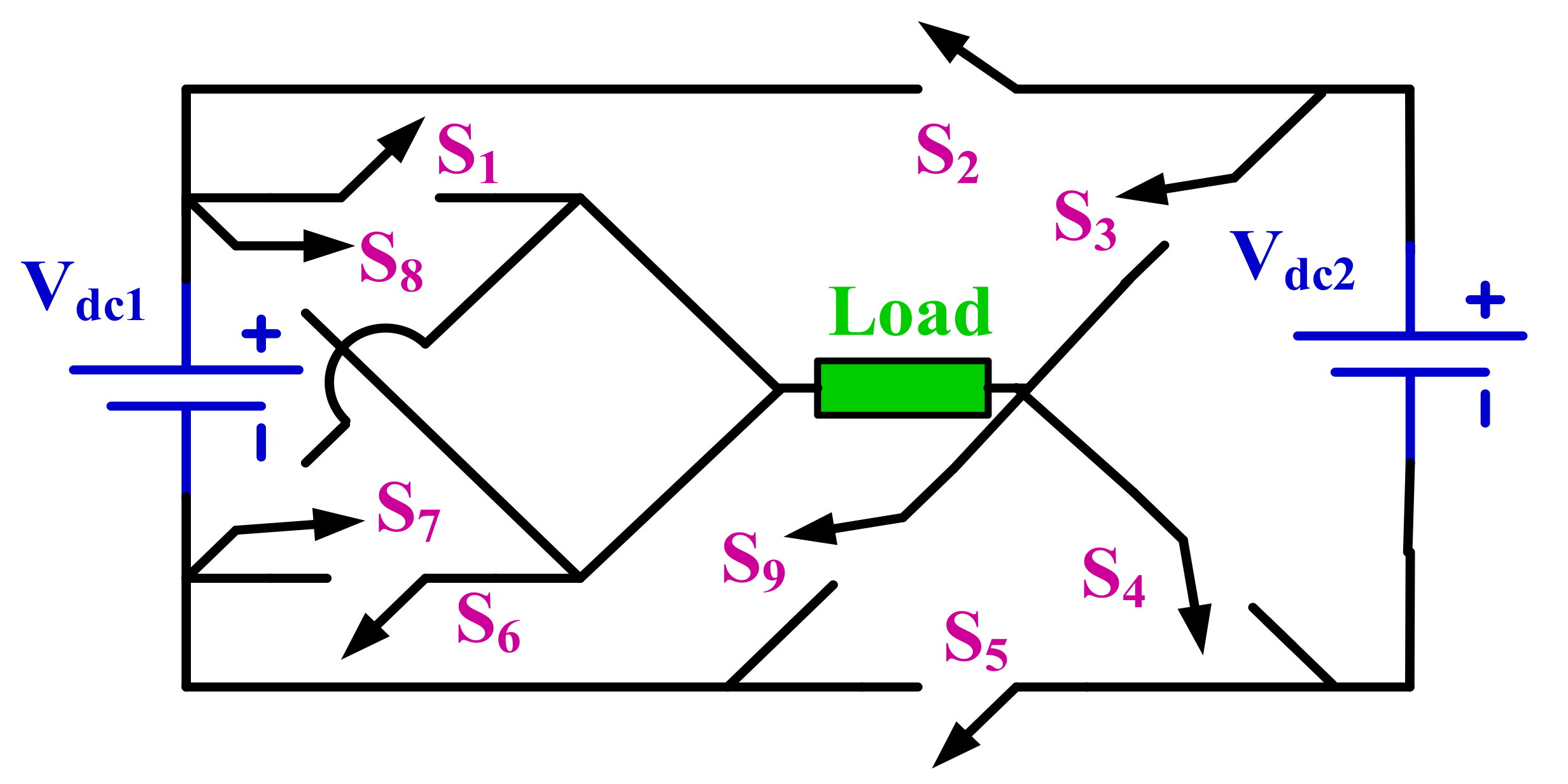
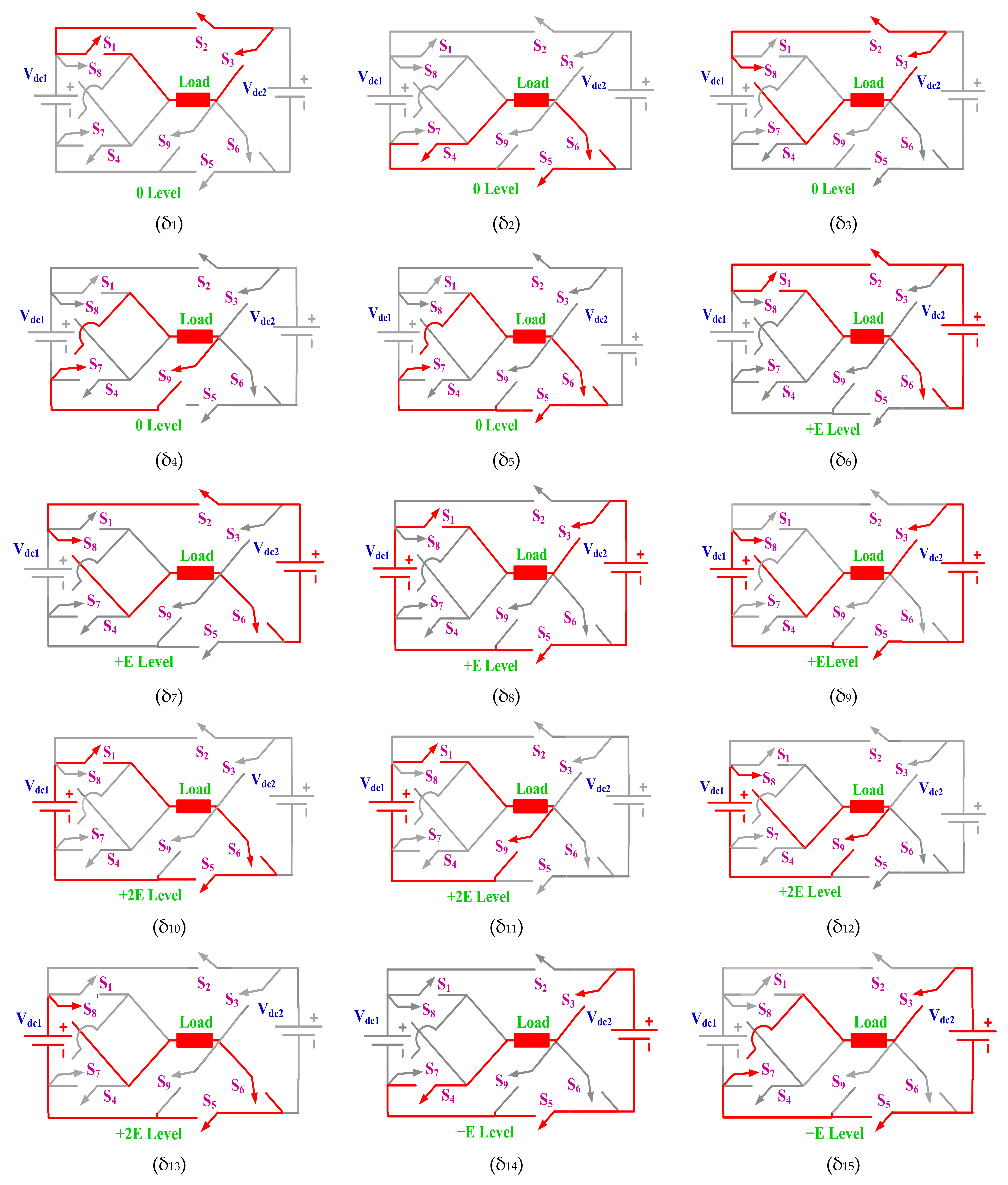
The proposed topology in this paper consists of nine active switches and two isolated DC sources, where the second source is fixed at half of the first DC source as shown in Figure 2. Switches S7, S8, and S9 are added to this circuit to provide more redundant paths for each output voltage level. As the number of redundant paths increases, the circuit has additional paths to obtain the required voltage if there is a fault in any switch of the circuit. The proposed five-level topology counters the drawback of experiencing a complete shutdown during the failure (OC) in switches S1 and S4. The output voltage level reduces to three-level during the failure in switches S2 and S3. The switching table of the proposed topology is provided in Table 2. Table 3 shows the potential switching states and viable output voltage levels if any switch from S1 to S9 fails (OC fault), taking one switch faulty at a time. As an example, if switch S1 fails, all of the five levels can be synthesized using one of the modes for each level from δ2, δ3, δ4, δ5, δ8, δ9, δ12, δ13, δ14, δ15, δ16, δ17, δ18, δ19, and δ20, as shown in Figure 3.

3. Conventional Nearest Level Control (NLC)

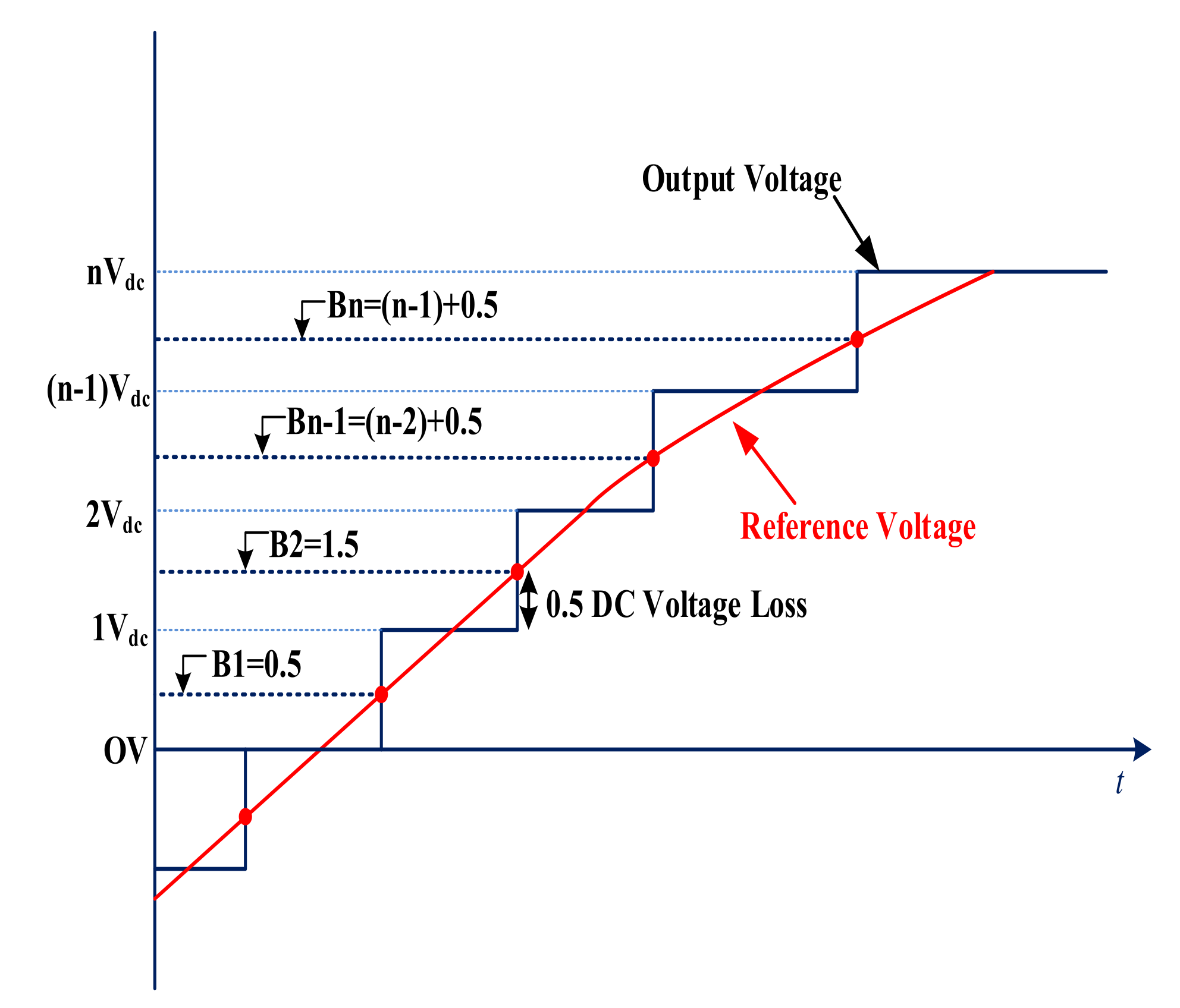
Modulation techniques play a crucial role in affecting switching loss, harmonics, and filter size. Conventional modulation methods have higher complexity, high switching loss, and increased switching harmonics as the number of submodules increases. The NLC has the advantage of low switching losses and minimum low order harmonics for higher output voltage applications. In the conventional NLC technique, a sinusoidal signal is used as a reference (Vref) signal, as shown in Figure 4 [10], which is compared with other carrier signals (B1 to Bn). The conventional procedure is presented in [11]. In this, 0.5Vdc DC loss error is always maintained between two levels. The working principle is depicted in Figure 5.
For N levels:
The total number of carrier signals (B1 to Bn) is expressed as
B 1 0.5   B 2 1 + 0.5   B 3 2 + 0.5   B 3 3 + 0.5     B n 1 n 2 + 0.5   B n n 1 + 0.5
where n = ( N l e v e l 1 ) / 2 .
The output voltage is
V o u t = m N l e v e l 1 2 V d c cos ω t  
where m refers to the modulation index and is expressed as
m = V r e f m a x / n V d c
The switching angles for the conventional NLC are given by
θ j = sin 1 j 0.5 / n
where j = 1 , 2 , 3   .   .   .   .   .   .   .   . ( N l e v e l 1 ) / 2 .

4. Power Loss Analysis

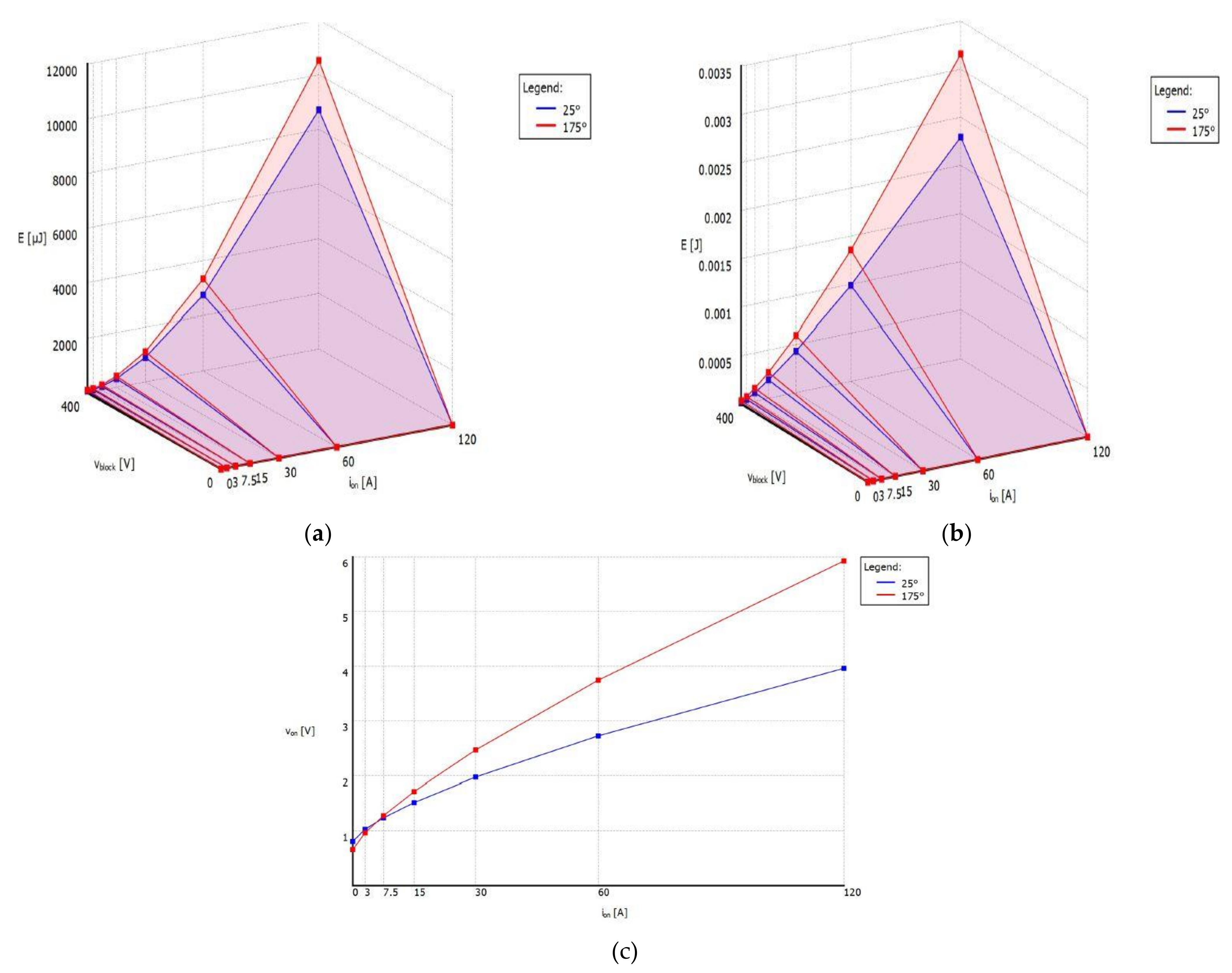
PLECS software has been used to calculate the power loss and efficiency, and the software’s thermal modelling is used to correctly determine conduction and switching losses for all switches. Infineon’s IGBT switch IGA30N60H3 was chosen for this investigation. Figure 6 depicts the IGBT’s turn on, turn off, and conduction loss models, respectively, and two types of losses were considered, i.e., the switching losses (PS) and conduction losses (PC) of all the semiconductor devices.

4.1. Switching Losses (PS)

Switching losses occur when the switches turn on or off [12,13]. Switching losses can be calculated by using the equations below.
The power loss during the interval of switching on is expressed by
P S ,   o n ,   n = f 0 t o n v t i t d t = f 0 t o n V S , n t o n t I n t o n t t o n d t =   1 6   f   V S , n I n t o n
The power loss during the interval of switching off is expressed by
P S ,   o f f ,   n = f 0 t o f f v t i t d t = f 0 t o f f V S , n t o f f t I n t o f f t t o f f d t =   1 6   f   V S , n I n t o f f
where I n and I n , respectively, signify currents across the nth switch when it was turned on and before it was turned off. V S , n specifies the voltage for the off-state of the nth switch, and f denotes the switching frequency. The on and off losses are summed to calculate the total switching loss:
P S = k = 1 9 m = 1 N o n P S , o n , n m + m = 1 N o f f P S , o f f , n m

4.2. Conduction Losses (PC)

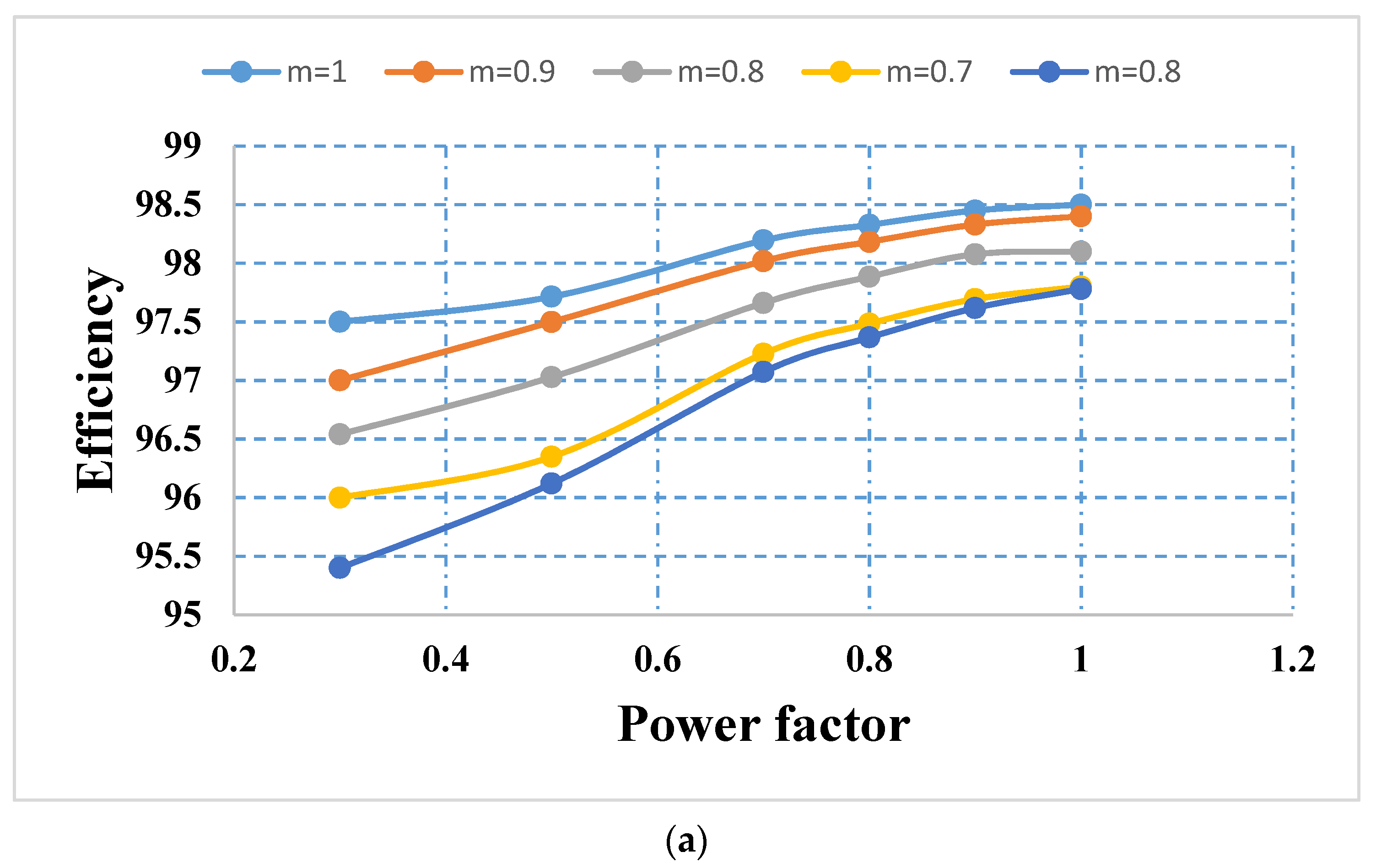
The losses due to the internal resistance of each semiconductor component are used to calculate the losses that occur due to them. Results are obtained for the resistive load by using the PLECS software. Figure 7a shows the efficiency versus power factor curve from which we observe that efficiency will be at a maximum when the modulation index equals one, and efficiency will decrease as the modulation index decreases. Figure 7b shows the power loss vs. power factor curve as we observe that power loss will be more for modulation index equals one and continues decreasing as we decrease the modulation index. Figure 7c shows the variation of THD with a change in the modulation.

5. Simulation Results and Discussions

The Simulink model of the proposed five-level fault-tolerant topology was developed using Matlab2018a, and for verifying the simulation results obtained, experimental hardware results were also recorded.

Simulation Results

The output voltage, load current, and THD for the (RL) load during the normal condition are simulated in the modified FT-MLI, as well as the output voltage and load current for the fault in each switch. The simulation is carried out using MATLAB/Simulink. Table 4 lists all of the device parameters used in the simulation. The magnitude of the DC voltage sources for simulation purposes was considered to be 100 and 50 volts. The output voltage and current, as shown in Figure 8a, are obtained at Z = 100 Ω + 318 mH during the normal condition, and the number of output voltage levels was reduced to three, as shown in Figure 8b when the modulation index changed from 1 to 0.5. This shows that the number of voltage levels is dependent on the modulation index. The THD of the output voltage at 50Hz is 16.12%, which is shown in Figure 8c.
The simulation results, as shown in Figure 9, are obtained when a fault in each switch of the proposed fault-tolerant topology occurs. In Figure 9, pre-fault, during-fault, and after-fault conditions have been shown. Pre-fault refers to the normal operation when no fault has occurred. During-fault refers to the system when the fault occurs to the circuit. Figure 9a shows the output waveform during the fault in switch S1 in which the output voltage regains its level after the fault. Figure 9b shows the output waveform when the fault occurs in switch S2, where the output voltage level reduces to three-level. Figure 9c shows the output waveform when there is a fault in switch S3, reducing the output voltage to three-level. Figure 9d shows the output waveform due to a fault in switch S4, which maintains the output voltage at five-level. Figure 9e shows the output waveform due to a fault in switch S5, which maintains the output voltage at five-level. Figure 9f shows the output waveform due to a fault in switch S6, which maintains the output voltage at five as the fault occurs. Figure 9g shows the output waveform due to a fault in switch S7, which maintains the output voltage at five-level. Figure 9h shows the output waveform due to a fault in switch S8, which maintains the output voltage at five-level. Figure 9i shows the output waveform due to a fault in Switch S9, which maintains the output voltage at five-level.

6. Experimental Setup and Results

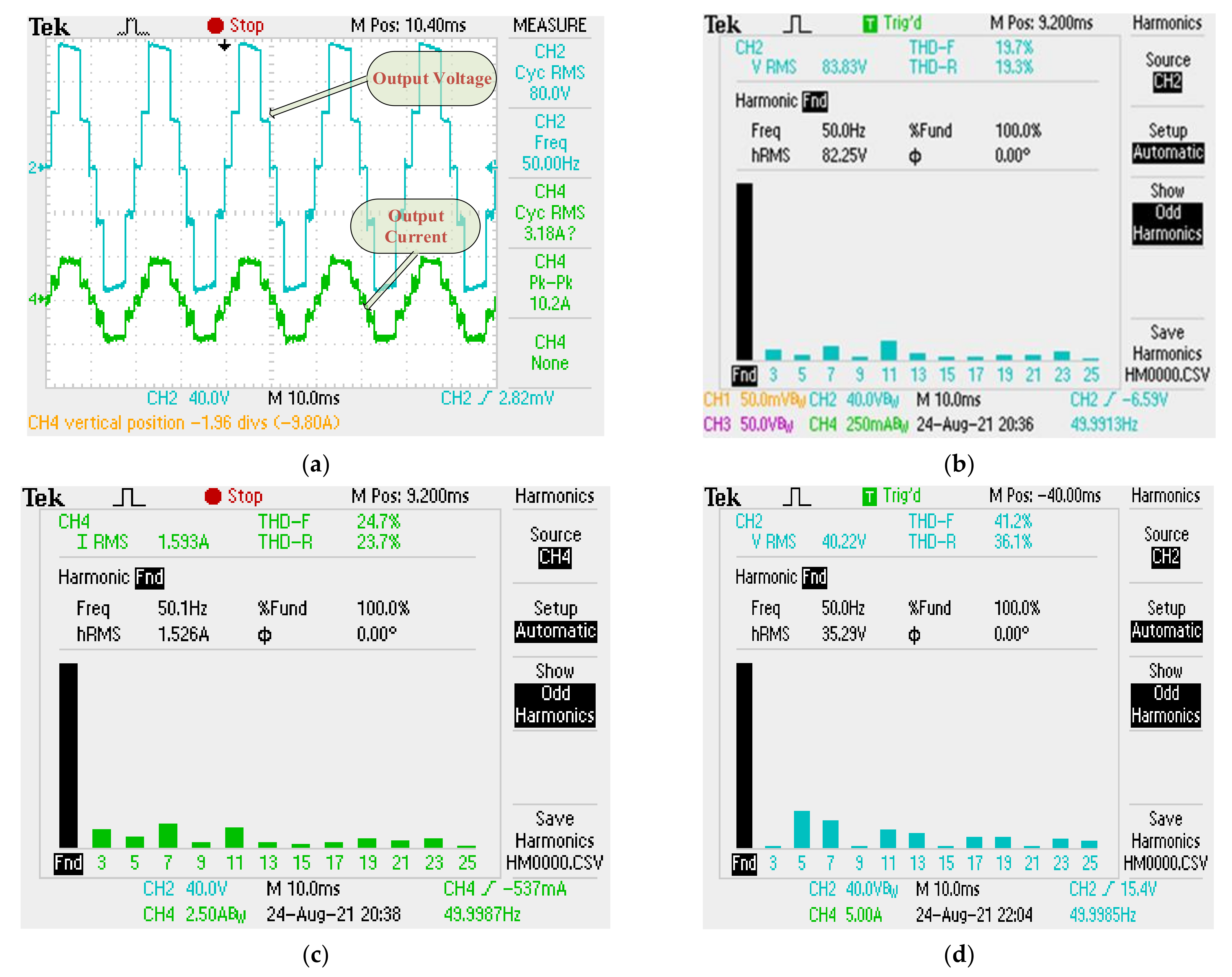
A hardware setup has been designed to test the feasibility and resilience of the proposed FT topology. An experimental model testing setup is shown in Figure 10. Through the gate driver TLP250 (F) and a DSP real-time controller that works as an interface with MATLAB/Simulink, control signals are provided to operate the IGBTs (IGBTFGA25N120) of discrete power switching modules. Two DC sources of 120 and 60 volts, respectively, are used in the hardware setup to obtain the result at a load of R = 300 Ω. Figure 11a shows the output voltage and current during normal conditions with a step size of 40 V and a peak output voltage of 80 Vrms. The output current shown in the figure has a peak-to-peak current of 10.2 A. Figure 11b shows the THD of the output voltage for five-level in which the fundamental THD is 19.7%. Only odd-order harmonics are produced. Even-order harmonics are absent. Figure 11c shows the THD of the output current when the output is five-level. The THD of the fundamental output current is 24.7%. Figure 11d shows the THD of the output voltage when the levels of the output voltage are reduced to three-level. The THD of the fundamental output voltage is 41.2%. Table 5 lists all of the device parameters used in the experiment.
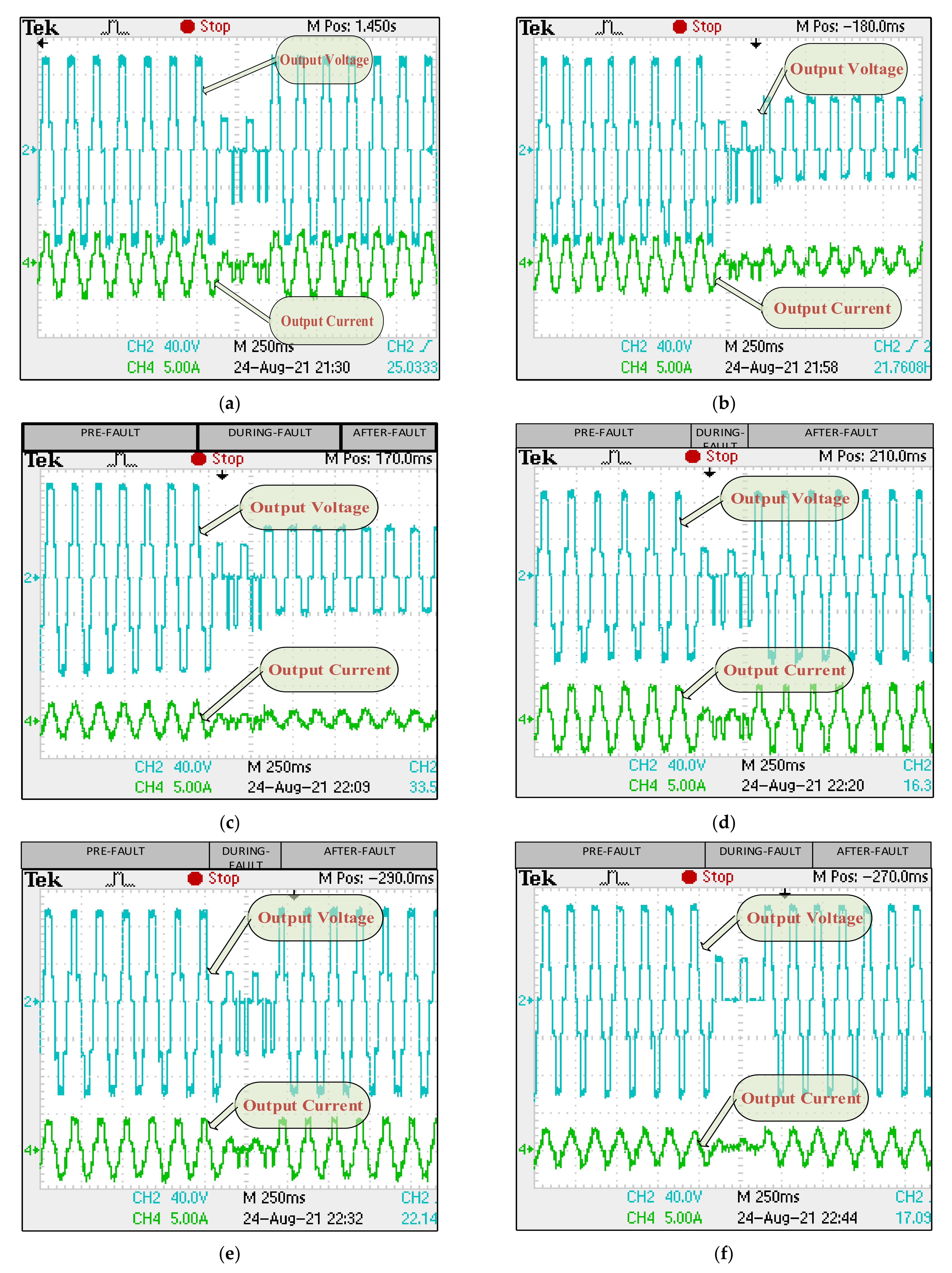
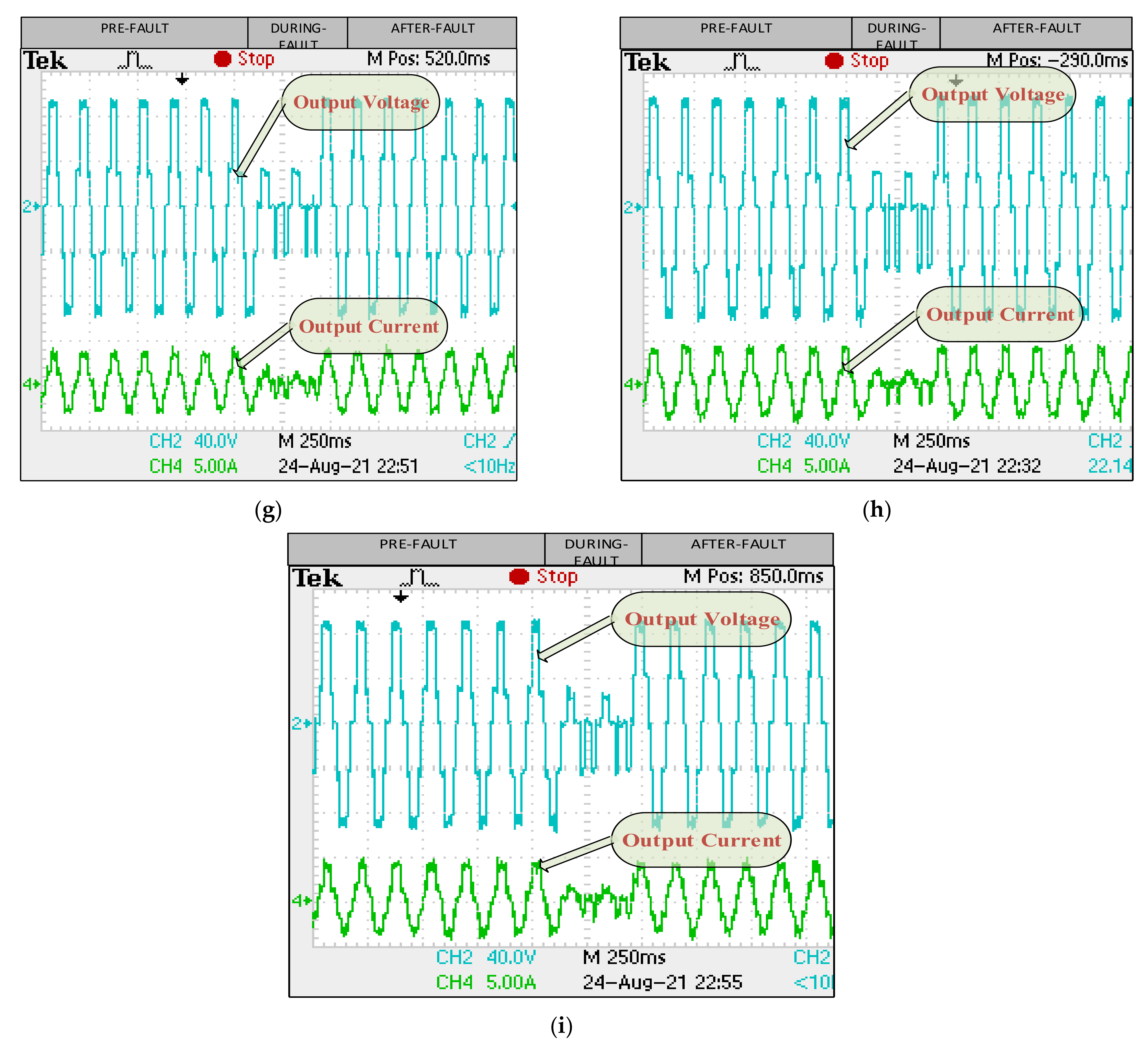
The output voltage and current waveforms during the fault condition, when the OC fault occurs at any switch, are shown in Figure 12. The output voltage and the output current are shown in Figure 12a when there is a fault in switch S1. The voltage and current have an 80V (rms) peak and a 10.2 A peak-to-peak value, respectively. Figure 12b shows the output waveforms (voltage and current) when there is a fault in switch S2. The output waveforms obtained are of three-level after a fault condition. Figure 12c shows the output waveforms when there is a fault in switch S3. The output waveforms obtained are of three-level. Figure 12d shows the output waveforms when there is a fault in switch S4. The output waveforms obtained are of five-level. Figure 12e shows the output waveforms when there is a fault in switch S5. The output waveforms obtained are of five-level. Figure 12f shows the output waveforms due to a fault in S6. The output waveforms obtained are of five-level. Figure 12g shows the output waveforms when there is a fault in switch S7. The output waveforms obtained are of five-level. Figure 12h shows the output waveforms when there is a fault in switch S8. Figure 12i shows the output waveforms when there is a fault in switch S9.

7. Inverter Topologies Comparison

In Table 6, a comparison of the component count of single-phase five-level conventional topology has been made to the proposed fault-tolerant topology with respect to the DC source, capacitor, clamped diode, and active switches. Cascaded H-bridge inverters do not require a clamping diode or balancing capacitor, and their control complexity is low. Flying capacitors and neutral point diode-clamped MLIs have the disadvantage of requiring many capacitors and diodes to produce higher levels and very high control complexity. PUC5 does not require a clamping diode and has the advantage of a self-balancing capacitor with a low control complexity. Table 7 summarizes the different figures of merit considered for the comparative study with fault-tolerant topology. A comparison is made between the number of main switches, flying capacitors, DC bus capacitors, clamping diodes, and main diodes. The number of power switches plays a vital role in dictating the overall size and cost of the inverter. As the number of switches and other components increases, the overall cost, size, and complexity of the circuit also increase. A higher number of switches also increases the switching and conduction loss, which deteriorates the overall efficiency of the circuit. In Table 7, the proposed topology does not require a clamping diode, main diode, DC bus capacitor, additional auxiliary module, redundant leg, or impedance network, which reduces the circuit complexity and the total number of switches required, providing an advantage over the other published topologies. The cost factor (CF), which is used to compare the cost-per-level of the output voltage, is given as [14,15]. The CF for the proposed topology is comparable with PUC5 and the cascaded H-bridge, even though it has fault-tolerant capability and is far better than the other remaining topologies. In Figure 13, the simulation result of PUC5 demonstrates the depreciation in the output power quality when the topology is not fault-tolerant.
Cost   Factor = No . of   DC   voltage   source + Capacitor + Clamped   Diode No . of   Switches No . of   output   Voltage   Level

8. Conclusions

This paper proposed a modified five-level fault-tolerant topology. By strategically putting three power switches in the circuit, the changed topology is obtained from the existing (five-level) topology which results in redundant paths. These redundant pathways can still provide output in the event of power switch open-circuit faults, conferring fault-tolerant properties and making the architecture fully fault-tolerant. In addition, under healthy, faulty, and post-fault operation, the updated FT-MLI topologies have two DC sources, with the second DC source set at half the value of the first DC voltage source. The control scheme has been operated using the nearest level control technique. The working principle and its flexibility against open-circuit failures have been proven by simulation and experimental results. The simulation, coupled with the experimental data, confirmed the modified FT-MLI topology's feasibility and effectiveness. Furthermore, a comparison with recently published topologies shows the effectiveness of the proposed topology.

Author Contributions

Conceptualization, M.A., M.T. and A.S.; Formal analysis, M.T., A.S., M.R.H. and S.A.; Investigation, M.A., M.T., A.S., L.M.-P. and A.S.N.M.; Methodology, M.T. and A.S.; Supervision, M.T. and A.S.; Writing—original draft, M.A. and M.R.H.; Writing—review and editing, M.T., A.S., S.A., L.M.-P. and A.S.N.M. All authors have read and agreed to the published version of the manuscript.

Funding

The authors extend their appreciation to King Saud University for funding this work through the Researchers Supporting Project number (RSP-2021/387), King Saud University, Riyadh, Saudi Arabia.

Conflicts of Interest

The authors declare no conflict of interest.

References

  1. Kouro, S.; Malinowski, M.; Gopakumar, K.; Pou, J.; Franquelo, L.G.; Wu, B.; Rodriguez, J.; Pérez, M.A.; Leon, J.I. Recent advances and industrial applications of multilevel converters. IEEE Trans. Ind. Electron. 2010, 57, 2553–2580. [Google Scholar] [CrossRef]
  2. Rodriguez, J.; Lai, J.-S.; Peng, F.Z. Multilevel inverters: A survey of topologies, controls, and applications. IEEE Trans. Ind. Electron. 2002, 49, 724–738. [Google Scholar] [CrossRef] [Green Version]
  3. Agrawal, R.; Jain, S. Comparison of reduced part count multilevel inverters (RPC-MLIs) for integration to the grid. Int. J. Electr. Power Energy Syst. 2017, 84, 214–224. [Google Scholar] [CrossRef]
  4. Tolbert, L.M.; Peng, F.Z.; Habetler, T.G. Multilevel inverters for electric vehicle applications. IEEE Work. Power Electron. Transp. 1998, 79–84. [Google Scholar] [CrossRef] [Green Version]
  5. Vahedi, H.; Labbé, P.A.; Al-Haddad, K. Sensor-Less Five-Level Packed U-Cell (PUC5) Inverter Operating in Stand-Alone and Grid-Connected Modes. IEEE Trans. Ind. Inform. 2016, 12, 361–370. [Google Scholar] [CrossRef]
  6. Khoucha, F.; Lagoun, M.S.; Kheloui, A.; Benbouzid, M.E.H. A comparison of symmetrical and asymmetrical three-phase H-bridge multilevel inverter for DTC induction motor drives. IEEE Trans. Energy Convers. 2011, 26, 64–72. [Google Scholar] [CrossRef] [Green Version]
  7. Zhang, W.; Xu, D.; Enjeti, P.N.; Li, H.; Hawke, J.T.; Krishnamoorthy, H.S. Survey on Fault-Tolerant Techniques for Power Electronic Converters. IEEE Trans. Power Electron. 2014, 29, 6319–6331. [Google Scholar] [CrossRef]
  8. Li, C.; Jiao, D.; Jia, J.; Guo, F.; Wang, J. Thermoelectric Cooling for Power Electronics Circuits: Modeling and Active Temperature Control. IEEE Trans. Ind. Appl. 2014, 50, 3995–4005. [Google Scholar] [CrossRef]
  9. Yang, Y.; Wang, H.; Blaabjerg, F. Improved Reliability of Single-Phase PV Inverters by Limiting the Maximum Feed—In Power. In Proceedings of the 2014 IEEE Energy Conversion Congress and Exposition (ECCE), Pittsburgh, PA, USA, 14–18 September 2014; pp. 128–135. [Google Scholar]
  10. Hussan, M.R.; Sarwar, A.; Siddique, M.D.; Mekhilef, S.; Ahmad, S.; Sharaf, M.; Zaindin, M.; Firdausi, M. A novel switched-capacitor multilevel inverter topology for energy storage and smart grid applications. Electronics 2020, 9, 1703. [Google Scholar] [CrossRef]
  11. Hu, P.; Jiang, D. A Level-Increased Nearest Level Modulation Method for Modular Multilevel Converters. IEEE Trans. Power Electron. 2015, 30, 1836–1842. [Google Scholar] [CrossRef]
  12. Hussan, M.R.; Sarwar, A.; Siddique, M.D.; Iqbal, A.; Alamri, B. A Cross Connected Asymmetrical Switched-Capacitor Multilevel Inverter. IEEE Access 2021, 9, 96416–96429. [Google Scholar] [CrossRef]
  13. Hussan, M.R.; Sarwar, A.; Khan, I.; Tariq, M.; Tayyab, M.; Alhosaini, W. An Eleven-Level Switched-Capacitor Inverter with Boosting Capability. Electronics 2021, 10, 2262. [Google Scholar] [CrossRef]
  14. Ye, Y.; Chen, S.; Wang, X.; Cheng, K.E. Self-Balanced 13-Level Inverter Based on Switched-Capacitor and Hybrid PWM Algorithm. IEEE Trans. Ind. Electron. 2020, 68, 4827–4837. [Google Scholar] [CrossRef]
  15. Tayyab, M.; Sarwar, A.; Khan, I.; Tariq, M.; Hussan, M.R.; Murshid, S.; Alhosaini, W. A single source switched-capacitor 13-level inverter with triple voltage boosting and reduced component count. Electronics 2021, 10, 2321. [Google Scholar] [CrossRef]
  16. Aly, M.; Ahmed, E.M.; Shoyama, M. A New Single-Phase Five-Level Inverter Topology for Single and Multiple Switches Fault Tolerance. IEEE Trans. Power Electron. 2018, 33, 9198–9208. [Google Scholar] [CrossRef]
  17. Mhiesan, H.; Wei, Y.; Siwakoti, Y.P.; Mantooth, H.A. A Fault-Tolerant Hybrid Cascaded H-Bridge Multilevel Inverter. IEEE Trans. Power Electron. 2020, 35, 12702–12715. [Google Scholar] [CrossRef]
  18. Nistane, T.J.; Sahu, L.K.; Jalhotra, M.; Gautam, S.P. Single and multiple switch fault-tolerance capabilities in a hybrid five-level inverter topology. IET Power Electron. 2020, 13, 1257–1266. [Google Scholar] [CrossRef]
  19. Li, J.; Huang, A.Q.; Liang, Z.; Bhattacharya, S. Analysis and design of active NPC (ANPC) inverters for fault-tolerant operation of high-power electrical drives. IEEE Trans. Power Electron. 2012, 27, 519–533. [Google Scholar] [CrossRef]
  20. Katebi, R.; He, J.; Weise, N. Investigation of Fault-Tolerant Capabilities in an Advanced Three-Level Active T-Type Converter. IEEE J. Emerg. Sel. Top. Power Electron. 2019, 7, 446–457. [Google Scholar] [CrossRef] [Green Version]
Figure 1. Classification of multilevel inverters.
Electronics 10 03099 g001
Figure 2. Proposed five-level fault-tolerant topology.
Electronics 10 03099 g002
Figure 3. All twenty switching states of proposed five-level fault-tolerant topology.
Electronics 10 03099 g003aElectronics 10 03099 g003b
Figure 4. Level generation.
Electronics 10 03099 g004
Figure 5. Simplified NLC.
Electronics 10 03099 g005
Figure 6. (a) Turn on loss, (b) turn off loss, and (c) conduction loss.
Electronics 10 03099 g006
Figure 7. (a) Modulation index vs. efficiency, (b) modulation index vs. power loss, and (c) modulation index vs. THD.
Electronics 10 03099 g007aElectronics 10 03099 g007b
Figure 8. (a) Simulation results for output voltage and load current during normal condition, (b) output voltage and load current at modulation index 1 and 0.5, and (c) THD of voltage during normal conditioning.
Electronics 10 03099 g008
Figure 9. (a) Fault in Switch S1/S1 S4, (b) fault in switch S2, (c) fault in switch S3, (d) fault in switch S4, (e) fault in switch S5, (f) fault in switch S6, (g) fault in switch S7/S1 S7, (h) fault in switch S8/S1 S8, (i) fault in switch S9/S1 S9, and (j) output of PUC5 result in normal condition.
Electronics 10 03099 g009
Figure 10. Hardware setup of the proposed topology.
Electronics 10 03099 g010
Figure 11. (a) Output voltage (V) and load current (A) during normal condition, (b) THD of output voltage for five-level, (c) THD of output current for five-level, and (d) THD of output voltage for three-level.
Electronics 10 03099 g011
Figure 12. (a) Fault in switch S1, (b) fault in switch S2, (c) fault in switch S3, (d) fault in switch S4, (e) fault in switch S5, (f) fault in switch S6, (g) fault in switch S7, (h) fault in switch S8, and (i) fault in switch S9.
Electronics 10 03099 g012aElectronics 10 03099 g012b
Figure 13. Pre-fault and post-fault output voltage and current waveform for PUC5.
Electronics 10 03099 g013
Table 1. Comparison of component count for conventional topologies.
Inverter ConfigurationDiode-ClampedFlying CapacitorCascaded Inverter
Switches2(t − 1)2(t − 1)2(t − 1)
Main Diodes2(t − 1)2(t − 1)2(t − 1)
Clamping Diodes(t − 1)(t − 2)00
DC Bus Capacitor(t − 1)(t − 1)(t − 1)/2
Balancing Capacitor0(t − 1)(t − 2)/20
Table 2. Switching table of proposed five-level fault-tolerant topology.
LevelsS1S2S3S4S5S6S7S8S9
111000000
000111000
011000010
0000000011
000011100
Vdc2110001000
010001010
(Vdc1−Vdc2)101010000
001010010
100000001
Vdc1100011000
000011010
000000011
010001100
001010100
−Vdc2001110000
010001100
− (Vdc1−Vdc2)010101000
−Vdc1011100000
011000010
Table 3. Different modes for any single switch OC fault in proposed five-level fault-tolerant topology.
Failed SwitchAvailable ModesOperation Level
S1δ2, δ3, δ4, δ5, δ8, δ9, δ12, δ13, δ14, δ15, δ16, δ17, δ18, δ19, δ205
S2δ2, δ3, δ5, δ7, δ9, δ10, δ13, δ12, δ13, δ14, δ15, δ16, δ17, δ18, δ19, δ203
S3δ1, δ3, δ4, δ5, δ6, δ7, δ8, δ9, δ10, δ11, δ12, δ13, δ14, δ16, δ183
S4δ1, δ3, δ4, δ5, δ6, δ7, δ8, δ9, δ10, δ11, δ12, δ13, δ14, δ16, δ185
S5δ1, δ4, δ5, δ6, δ8, δ10, δ11, δ13, δ14, δ15, δ16, δ18, δ19, δ205
S6δ1, δ4, δ5, δ7, δ9, δ10, δ13, δ15, δ17, δ19, δ205
S7δ1, δ2, δ4, δ6, δ7, δ8, δ9, δ10, δ11, δ12, δ13, δ15, δ18, δ195
S8δ1, δ2, δ3, δ5, δ6, δ7, δ10, δ11, δ14, δ15, δ16, δ17, δ18, δ19, δ205
S9δ1, δ2, δ3, δ4, δ6, δ7, δ8, δ9, δ11, δ12, δ14, δ15, δ16, δ17, δ18, δ19, δ205
Table 4. Parameters used for simulation.
ParametersSpecification
DC Supply 1100
DC Supply 250
Load Resistance and Inductance ValueR = 100 Ω, L = 318 mH
Modulation Index1
Switching Frequency50 HZ
Table 5. Parameters for experimental validation.
ParametersSpecification Type
DC Voltage Source 160
DC Voltage Source 230
SwitchesIGBTFGA25N120
Resistive Load300 Ω
DSP KitC2000, Texas
OptocouplerTLP250(TOSHIBA)
Modulation Index(M)1
Switching Frequency50 HZ
Table 6. Comparison table for single-phase five-level.
Inverter TypeDC SourcesCapacitorClamped DiodeActive SwitchTotal Parts CountControl ComplexityCost Factor
Cascaded-H Bridge200810Low3.2
NPC with Voltage Control146819Very High17.6
NPC without Voltage Control406818Low16
Flying Capacitor130610High4.8
PUC511068Very Low2.4
Proposed Topology200911Very Low3.6
Table 7. Comparison of the total parts count for the proposed fault-tolerant topology with the existing topology.
Inverter Configuration[16][17][18][19][20]Proposed Topology
Main Switches14161218129
Main Diodes14161218120
Clamping Diodes400000
DC Bus Capacitor000200
Flying Capacitor000100
Voltage Level in Healthy Condition575335
DC Voltage Sources231122
Cost Factor5643.4231.2138563.6
Bi-directional Switches000000
Auxiliary Module
Redundant Leg
Impedance Network
SingleSwitch OCFaultTolerant
Publisher’s Note: MDPI stays neutral with regard to jurisdictional claims in published maps and institutional affiliations.