1. Introduction
When distributed generation is connected to the grid, the DC microgrid can provide a flexible and efficient basic distribution layer. The DC microgrid has received more and more attention for avoiding the conversion of multi-stage power electronic converters such as AC/DC and DC/AC, as well as the complex frequency and reactive power regulation problems [
1,
2,
3].
The main control goal of the DC microgrid is the stability of the DC bus voltage. Compared to master-slave control, which relies on high-speed communication technology, droop control does not require communication [
4]. DC microgrid systems with droop control have higher reliability and can easily realize power distribution and voltage regulation among multiple sources [
5,
6]. However, the DC microgrid is composed of a large number of power electronic converters, and its inertia is insufficient. When it is disturbed, it is easy to cause large dynamic voltage fluctuations [
7,
8]. Therefore, it is not only necessary to consider improving the transient control performance of the voltage closed-loop but also to analyze and solve the problem of insufficient system inertia when designing a DC microgrid bus voltage controller. Although increasing the DC bus capacity can increase the inertia of the DC microgrid and reduce the voltage transient caused by the sudden change of source load power, and it is beneficial to the system’s stable operation effect. However, considering the high cost and large volume of power capacitors, the concept of virtual inertia is a major alternative [
9,
10].
The concept of virtual inertia comes from the AC microgrid, which is based on the virtual inertia compensation of virtual synchronous generators. The DC microgrid learns from it and uses the equivalent concept to improve inertia. In the AC microgrid, the realization of virtual inertia utilizes the change of the frequency, while in the DC microgrid, it is realized by the change of the DC voltage. To reasonably use the degree of voltage change and compensate the system with appropriate virtual inertia, this paper proposes a variable droop coefficient nonlinear virtual inertia control method considering the voltage change rate. The droop control method used by the converter is equivalent to the series virtual impedance [
11]. It uses load fluctuation feedback to affect the nonlinear change of the droop coefficient, and the bus makes nonlinear adjustments regarding the output voltage. As a result, the voltage stabilization inertia of the distributed power supply with the buck–boost converter interface is improved.
In addition, the DC/DC converter is a key executive component in the DC microgrid, and it is used for the output power control and the voltage regulation of distributed generation. There are many types of DC/DC converters. Among them, the traditional buck–boost converter has both a buck–boost function, and it has the advantages of a small number of components and low cost. The buck–boost converter has been widely used in various fields of research, such as energy storage systems, electric vehicle drives systems, photovoltaic power generation systems, etc. However, the buck–boost converter is a highly nonlinear system; there is a right half-plane zero in the classic control theory. Therefore, we need to explore the nonlinear control method of the converter more deeply to improve the outstanding high-frequency dynamic output characteristics of the converter. This is not only an important issue that needs to be further resolved but also a key technology for stabilizing the DC bus voltage [
12,
13,
14,
15,
16,
17].
To solve the problem that negative incremental impedance of a constant power load can lead to system instability, a higher-order sliding mode control method based on a super-torque algorithm was proposed in the reference [
18]. In a medium-voltage DC integrated power system, it is experimentally demonstrated that the converter has strong robustness and reduced chattering in the system under the disturbances of sudden load changes, but the controller only involves single closed-loop voltage control and lacks regulation of the inductor current, which may cause current spikes during operating mode transitions. Reference [
19] studied the dynamic control characteristics of buck–boost converter based on hysteresis current. This reference uses a single closed-loop current-based method for power control. The characteristic of this controller is that the structure is simple and easy to realize.
However, there are usually two types of converter output voltage regulation control strategies, which are divided into single closed-loop and multi-closed-loop cascades. The cascade control method introduces internal current feedback to improve response speed and limit overcurrent [
20]. Because the multi-closed-loop cascade control method can integrate the advantages of multiple types of control strategies, it is more reliable and efficient. Reference [
21] proposed a multi-PI loop cascade control method for buck–boost converter. However, conventional PI control has some shortcomings: poor robustness, easy oscillation and saturation of the control volume. The external voltage loop and internal current loop in reference [
22] both adopt non-singular terminal sliding mode control. This control method is easy to meet the fixed switching frequency requirements and demonstrates the strong robustness of sliding mode control. The reference [
23] proposes a cascade control scheme with a conventional droop control method for the outermost control and an internal cascade control scheme consisting of a voltage derivative control inner loop and a voltage control outer loop. The control method achieves accurate power-sharing and proper voltage regulation of the DC microgrid in islanded operation mode. However, due to the presence of cable impedance, the traditional droop control suffers from a contradiction between voltage deviation and current distribution accuracy. In order to improve the limitations of conventional droop control, secondary control is proposed in the form of compensation to readjust the initial droop profile. A cascade control scheme consisting of virtual inertia control, recovery control and coordinated current sharing control is proposed in the reference [
24]. During grid-connected and off-grid operation of the DC microgrid, both transient and steady-state voltage conditions at the DC bus are significantly improved when there are abrupt changes at the supply and load sides. However, the control method does not take into account the nonlinear effects of virtual inertia control during mode switching. For multiple parallel buck–boost converters with parallel power supplies, the reference [
25] proposes a DC microgrid cascade control scheme with good scalability and robustness, which consists of a droop controller and an auxiliary controller, not only for current sharing between parallel power supplies, but also for compensating the voltage deviation caused by the main controller. However, the cascade control only involves the compensation control of voltage deviation, but not the regulation of inductor current, which cannot avoid the influence of inductor spike current to the system.
In recent years, control strategies based on sliding mode and backstepping have been widely used in various types of control systems due to their excellent adaptability and strong robustness. For nonlinear systems with uncertainty and external disturbances, the reference [
26] uses fuzzy neural networks to approximate unknown nonlinear functions and designs adaptive backstepping fuzzy neural sliding mode controllers. However, the fuzzy rule acquisition method in fuzzy neural networks is complex, and there is also a contradiction between the complexity of the model and the generalization ability. For boost converters containing constant power loads in DC microgrid, without an accurate mathematical model and without stable dynamic systems, a nonlinear control method combining an accurate feedback linearization technique with adaptive backstepping sliding mode control (ABSMC) is proposed in the reference [
27]. The method solves the instability problem caused by constant power loads, reduces the impact of sliding mode chattering on the system and ensures the stability of the DC bus voltage. However, the control method does not take into account the regulation of the inductor current, which may cause spikes, or the lack of inertia of the system. Reference [
28] designed a nonlinear backstepping sliding mode controller for airship trajectory tracking based on the disturbance observer. Simulation analysis shows that compared with traditional backstepping control and sliding mode control strategies, the proposed method is more robust in the three cases of unknown disturbance, model parameter uncertainty, and wind speed influence. However, the sliding mode control law often introduces the upper bound of the uncertainty term as the control coefficient of the switching function, which is easy to cause high-frequency and high-amplitude chattering of the output control quantity. To avoid this problem, an adaptive algorithm can be used to optimize it [
29].
In summary, the main contributions of this paper include: (1) Propose a nonlinear droop control law based on the converter output voltage variation rate dVdc/dt, which facilitates the voltage stability of the bus. (2) Propose an adaptive coefficient function that limits the converter output voltage variation rate, which has continuous, smooth, and saturated nonlinear characteristics. (3) Propose a three-level cascade control method that is based on a nonlinear virtual inertia control with droop variable coefficients and adaptive backstepping sliding mode voltage and current double closed-loop control. It achieves robust high stability of bus voltages in distributed multi-source DC microgrid. (4) Verify the feasibility and effectiveness of the proposed method by comparing the results with traditional control methods.
4. Design of Adaptive Backstepping Sliding Mode Controller
In this section, we design a voltage and current double closed-loop controller based on an adaptive backstepping sliding mode method. The adaptive backstepping sliding mode control method is a recursive design method with excellent adaptability. It involves the feedback control method and the judgment of the stability of the Lyapunov function. The proposed controller is designed in multiple steps and is not higher than the order of the system. The sliding mode control method has strong robustness, which limits the uncertainty of the system through the design of the sliding mode. The adaptive backstepping sliding mode control combines the advantages of the adaptive backstepping control method and the sliding mode control method to obtain good dynamic and static performance.
4.1. Design of Backstepping Sliding Mode Controller
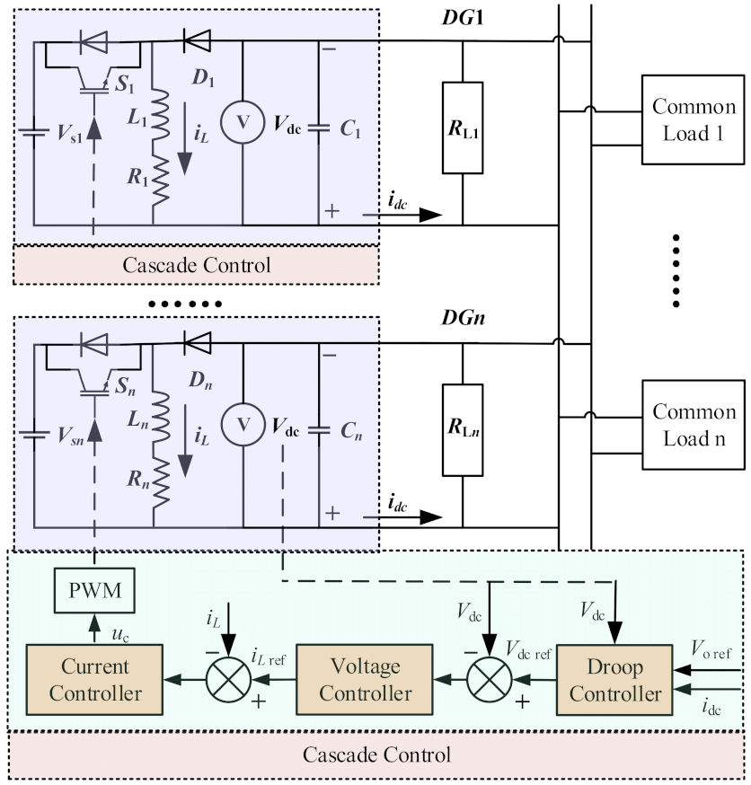
According to the cascade control structure shown in
Figure 1, the goal of the voltage and current backstepping sliding mode controller is to track the reference input. That is, the output voltage
Vdc of the converter tracks the given reference voltage
Vdc ref output by the previous stage virtual inertia controller. The current
iL flowing through the inductor
L of the converter tracks the given reference current
iL ref output by the previous stage voltage controller. Ensure that the above two tracking errors tend to zero. The backstepping sliding mode control design mainly includes two steps:
Define voltage tracking error
zV and current tracking error
zi as:
Define the virtual control variables of voltage tracking error
zV and current tracking error
zi as:
where
c1 and
c2 are adjustable design parameters.
Define the Lyapunov functions
VV1 and
Vi1 as
Define the new voltage tracking error
zV1 and current tracking error
zi1 as:
If zV1 = 0 and zi1 = 0, then . Therefore, this still needs to continue to the next step of design.
Further, define the Lyapunov functions
VV2 and
Vi2 as:
where
σV and
σi are respectively the sliding mode surface functions of the voltage controller and current controller, defined as:
where
k1 and
k2 are adjustable design parameters.
If
, the voltage backstepping sliding mode control law
iL ref and the current backstepping sliding mode control law
uc are designed as:
where
h1,
h2,
β1,
β2 are adjustable design parameters.
4.2. Design of Adaptive Backstepping Sliding Mode Controller
To suppress the influence of the external uncertain disturbance terms FV and Fi on the voltage and current control links, the sign function coefficients in Equations (32) and (33) often need to be conservatively designed. If we choose the upper bounds of FV and Fi, it will cause high-frequency chattering of the control law. Therefore, this section uses an adaptive algorithm to estimate FV and Fi in real-time.
Define the Lyapunov functions
VV3 and
Vi3 as:
where
and
are respectively the estimation errors of
and
, defined as:
where
and
are respectively the estimated values of
and
,
and
are the actual values of
and
, respectively.
From Equations (34) and (35), if
,
, then the adaptive law needs to be designed as:
where γ
1 and γ
2 are adjustable design parameters.
The design of the control law consists of determining the equivalent control law for the linear condition of the system and switching control law for the uncertain and disturbance terms. According to Equation (38), the equivalent control law
mV eq of the voltage controller is designed as:
The switching control law
mV s is:
Therefore, the voltage control law can be obtained
mV =
mV eq+
mV sAccording to Equation (39), the equivalent control law
mi eq of the current controller is designed as:
The switching control law
mi s is:
Therefore, the current control law can be obtained
mi =
mi eq+
mi sSubstituting Equations (38) and (40) into Equation (34),
Substituting Equations (39) and (41) into Equation (35),
where
,
,
By adjusting the values of h1, c1, k1, h2, c2, and k2, we can make |Q1| > 0, |Q2| > 0. To ensure that it is a positive definite matrix to make the system stable.
Therefore, from Equations (42) and (43), we obtain voltage controller
iL ref and current controller
uc as
5. System Simulation and Analysis
By using the MATLAB/Simulink platform, the correctness of the proposed control method is verified. For the DC microgrid distributed buck–boost converter interface circuit and controller shown in
Figure 1, we build models and do experimental analysis. The parameters of the DC microgrid system model are shown in
Table 1.
The experimental simulation scheme is divided into two types: voltage and current double closed-loop cascade control, and three-level cascade control with virtual inertia. In addition, traditional methods such as voltage and current linear PI control and steady droop control are designed to compare and analyze the new methods in this paper.
5.1. Voltage and Current Double Closed-Loop Cascade Control
This simulation program analyzes the performance of the adaptive backstepping sliding mode current and voltage control method of the buck–boost converter.
It is common that the response of the current inner-loop controller should be much faster than that of the voltage outer-loop controller. Therefore, according to this principle, the parameters of the current inner-loop controller are designed: (1) For ABSMC-based current loop controllers, β1 can be assumed to be one. (2) If h1 is too small, the system will go out of control; if h1 is too large, the time for the system to reach stability will increase significantly. (3) If r1 is too small, the system will also go out of control; if r1 is too large, the system will oscillate significantly and it will be difficult to reach stability. (4) If c1 is too small, the time for the system to reach stability will increase; if c1 is too large, the overshoot of the output voltage will increase significantly. (5) If k1 is too small, the system will be out of control; if k1 is too large, the overshoot of the output voltage will also increase significantly. Therefore, according to the criteria as above, the current controller parameters are designed based on the trial-and-error method. Similarly, the parameter design process for the voltage controller can be completed according to the above steps.
By coordinating and tracking the comprehensive performance of overshoot, response time, and stabilization time, this paper designs an adaptive backstepping sliding mode current and voltage controller parameters, as shown in
Table 2.
For comparison, this section designs a buck–boost converter current and voltage PI controller. The design of PI controller parameters is based on the following steps: (1) Establish a PI-based voltage and current double closed-loop controller model in Simulink. (2) Based on the converter switching frequency
fsw, the bandwidth of the current control loop should be much smaller than the converter switching frequency
fsw, set to
fsw/10 = 1 kHz; the bandwidth of the voltage control loop should be much smaller than the bandwidth of the current control loop, Set it to
fsw/100 = 100 Hz. (3) According to the above standards, use the “PID tuning tool” tool to debug the current and voltage double closed-loop PI control parameters as shown in
Table 3.
At the initial moment of the simulation, set the load RL = 200 Ω and the bus DC voltage reference value Vo ref = 0 V. At time 1, 2, and 3 s, Vo ref suddenly changed to 50, 100, 150 V, respectively; at time 4 s, RL suddenly changed to 100 Ω.
As shown in
Figure 6, when the voltage reference value and load change, this scheme compares the response performance of cascaded PI and cascaded ABSMC. As shown in
Figure 6a–e, the proposed cascaded ABSMC is compared with the traditional cascaded PI. In the 1–4 s period, while the response time is accelerated, the overshoot is reduced by about 1.5%, 0.8%, 0.4%, 0.8%, and there is no static error in the steady-state. When tracking the change of the voltage reference value, the proposed control method shows better transient and steady-state performance. Compared with the control method based on cascaded PI, the proposed control method based on cascaded ABSMC reflects lower overshoot, faster response speed, and shorter settling time under the effect of voltage tracking and load disturbance.
In addition, as shown in
Figure 6f, when the reference value of the bus voltage changes significantly, the peak current of the proposed control method based on cascaded ABSMC is much lower than that of the control method based on cascaded PI. In summary, compared with the traditional control method based on cascaded PI, the proposed control method based on cascaded ABSMC shows better transient and steady-state performance.
5.2. Three-Level Cascade Control with Virtual Inertia
This simulation program analyzes the performance of the proposed three-level cascade control method.
The parameter Q2 plays an important role in the nonlinear virtual inertia control method based on the variable droop coefficient. To better choose the parameter value of Q2, this scheme adopts the comparative analysis method to carry out a multi-parameter simulation comparison.
The bus DC voltage reference value Vo ref is set to change between 150–140 V in the 3rd and 4th seconds, and the Q2 value is selected as 1, 5, 10, 20, 50, 100 for simulation.
As shown in
Figure 7, with the increase of
Q2, when the bus reference voltage changes suddenly, the inertia of the converter output voltage also increases. However, when the reference value of the bus voltage changes, as
Q2 increases, it takes longer for the output reference voltage of the converter to establish a new steady state, which also means that the response speed of the proposed nonlinear virtual inertial control method will be slower.
Based on the above considerations, the parameter value of
Q2 is selected as 25 in this paper. The parameters of the proposed nonlinear virtual inertial droop control method are shown in
Table 4.
To verify the performance of the proposed three-level cascade control method, four different cascade control methods are designed for comparison: (i) Traditional droop control and current and voltage PI three-level cascade control (PIdroop); (ii) Virtual inertial droop control and current Voltage PI three-level cascade control (PIVIC); (iii) Traditional droop control and three-level cascade control of current and voltage ABSMC (ABSMCdroop); (iv) Virtual inertia droop control and current and voltage ABSMC three-level cascade control (ABSMCVIC).
To prove that the proposed three-level cascade control with virtual inertia has good tracking characteristics under the reference input step change, this scheme sets the bus DC voltage reference value Vo ref = 20 V. At 0.5 and 1.5 s moments, Vo ref respectively suddenly changed to 50 and 100 V; at 2.5 s and 3.5 s moments, Vo ref respectively suddenly changed to 50 and 20 V.
As shown in
Figure 8, the proposed control method shows better transient and steady-state performance when tracking the voltage reference value. Compared to other three-level cascade control methods, the proposed method exhibits lower overshoot, faster response speed and shorter settling time when tracking the voltage reference value.
Considering the impact of load mutation on the bus voltage, this scheme sets the initial time of simulation, load RL = 200 Ω, bus DC voltage reference value Vo ref =150 V. At the 3rd second moment, RL suddenly changes to 100 Ω; at the 4th second moment, RL suddenly changes to 200 Ω.
Figure 9 shows the output voltage of the converter when the above four different control methods respond to load changes. The performance parameters of four different control methods are shown in
Table 5. It can be seen from
Table 5 that the proposed three-level cascade control method with virtual inertia shows lower overshoot, shorter transition time and smaller IAE (Absolute error integration indicator) when responding to load changes and provides higher inertia for the output voltage of the converter.
5.3. Three-Level Cascade Control under Continuous Dynamic Changes
This scheme sets the voltage reference value
Vo ref to change continuously and dynamically within a small range of 90~110 V and a large range of 50~150 V. Under the three-level cascade control conditions based on virtual inertia droop control and current and voltage adaptive backstepping sliding mode control, the response curve of the converter output voltage
Vdc is shown in
Figure 10.
Figure 10a shows that the converter can track the voltage reference value accurately and achieve effective control of the output voltage when the DC bus voltage reference value
Vo ref varies continuously and dynamically in a small range.
Figure 10b shows that due to the capacitance of the capacitor, there is a slight delay in tracking the high-frequency voltage signal. But the trend of the response is consistent with the trend of the original signal of the voltage reference value, and finally tends to be stable.


