Article

Impacts of LaOx Doping on the Performance of ITO/Al2O3/ITO Transparent RRAM Devices

1
Key Laboratory for Wide Band Gap Semiconductor Materials and Devices of Education, School of Microelectronics, Xidian University, Xi’an 710071, China
2
State Grid Key Laboratory of Power Industrial Chip Design and Analysis Technology, Beijing Smart-Chip Microelectronics Technology Co., Ltd. Beijing 102200, China
*
Author to whom correspondence should be addressed.
Electronics 2021, 10(3), 272; https://doi.org/10.3390/electronics10030272
Submission received: 24 December 2020 / Revised: 18 January 2021 / Accepted: 20 January 2021 / Published: 23 January 2021
(This article belongs to the Section Semiconductor Devices)

Abstract

:
Fully transparent ITO/LaAlO3/ITO structure RRAM (resistive random access memory) devices were fabricated on glass substrate, and ITO/Al2O3/ITO structure devices were set for comparison. The electrical characteristics of the devices were analyzed by Agilent B1500A semiconductor analyzer. Compared with the ITO/Al2O3/ITO RRAM devices, the current stability, SET/RESET voltage distribution, and retention characteristic of the ITO/LaAlO3/ITO RRAM devices have been greatly improved. In the visible light range, the light transmittance of the device is about 80%, that of the LaAlO3 layer is about 95%, the on-off ratio of the device is greater than 40, and the data retention time is longer than 10,000 s. The devices have great optical and electrical properties and have huge application potential as fully transparent RRAM devices.

1. Introduction

With the vigorous development of global information technology and the continuous advancement of semiconductor process nodes, people’s demand for miniaturization, high speed, high capacity, and other aspects of non-volatile memory is increasingly high, and people begin to explore new storage devices. RRAM devices has attracted much attention due to its fabrication simplicity, fast reading and writing speed [1], low power consumption [2], and potential of 3D stacking [3,4]. RRAM cells are mostly a sandwich structure of Top Electrode (TE)-Resistive Switching (RS) Layer-Bottom Electrode (BE). Among them, the resistive switching layer plays a key role in the performance of the device. Materials that have been proven to have resistive characteristics include solid electrolyte materials [5,6], new nanomaterials [7,8], binary and multiple oxide materials [9,10,11], etc., among which metal oxide materials have many advantages such as simple structure and easy control of ingredients. Besides, lanthanum-based multielement oxide materials are more suitable because of their higher K value, larger bandgap width, and better thermal stability [12]. At present, it has been confirmed that HfLaO3 [13], La0.3Pr0.4Ca0.3MnO3 [14], and LaAlO3 [15] materials can be used as resistive switching material and obtain good performance. The work in this paper also used lanthanum-based oxide materials as the resistive switching layer for related research.
In the process of fabricating microelectronic devices, atomic layer deposition(ALD) technology is widely used in the fabrication process of integrated circuits due to the outstanding characteristics of the film prepared by it, such as good uniformity, good flatness, high control accuracy of thickness, mass production capacity and good compatibility with the current CMOS process [16,17]. The hafnium oxide, lanthanum oxide [18] and other dielectric layers have been prepared by atomic layer deposition device in the field of resistively variable memory and good performance has been obtained [19]. Therefore, this process is used to fabricate the resistive switching layer of transparent resistive memory in this paper.
Compared with traditional non-transparent devices, fully transparent devices are more widely used in the fields of solar cells [20,21], photovoltaic conversion equipment [22], and liquid crystal display [23] due to their excellent light transmittance in the visible light range. TRRAM (transparent resistive random access memory) devices based on rare earth oxides, transition metal oxides and nitrides using ITO (Indium Tin Oxide) as top and bottom electrodes, such as CeO2 [11], EuO2 [24], Gd:SiO2 [25], and Gd2O3 [26]. However, there is still less research about the transparent RRAM devices made of LaAlO3 materials fabricated by atomic layer deposition technology. In this study, we have investigated the resistive switching characteristics of RRAM devices based on a transparent ITO/LaAlO3/ITO capacitor structure. The possible resistive switching mechanism of our TRRAM devices have been proposed to be based on the formation and rupture of conducting filaments. The bipolar RS characteristics of the fabricated ITO/LaAlO3/ITO TRRAM devices are observed to be reliable and stable switching characteristics.

2. Materials and Methods

In the work of this article, the memory cell of the transparent RRAM is the key part of our research, namely the sandwich structure of Top Electrode-Resistive Switching Layer-Bottom Electrode. The fabrication process of this structure which is simple and compatible with the CMOS fabrication process will be introduced below.
The glass substrates (3 cm * 3 cm * 1.1 mm) were cleaned using acetone and absolute ethanol solution to ultrasonically for 20 min. Place the glass substrate in a magnetron sputtering device to fabricate an ITO film with a thickness of about 185 nm as the bottom electrode. The resistive switching (RS) layer was fabricated by the ALD system using La(i-PrCp)3 and Al(CH3)3 as precursors, ozone as oxidant at a temperature of 280 °C. By setting the pulse period of different precursors and adjusting the sequence of pulses, the resistive dielectric layer films of different structures are prepared. The ITO material of about 100 nm was prepared as the top electrode of the devices. After photolithography, the top electrode structure was formed by magnetron sputtering and lift-off. Thus, complete devices preparation process can be completed by the fabrication process shown in Figure 1. The electrical characteristics of the RRAM device are completed by the Agilent B1500A analyzer. As shown in Figure 1, one of the probes is connected to the top electrode of the device, and the other probe is connected to the bottom electrode and ground at the same time. The probe adopts the ST-20-5 probe made by GGB co. with a tip diameter of about 10 μm. The total contact resistance is about 16 Ω.
Two sample groups were set up: S1: ITO/Al2O3/ITO and S2: ITO/LaAlO3/ITO. The alumina resistive switching layer of S1 devices was made by growing 230 cycles of ALD equipment; in order to ensure the same thickness of the RS layer, the resistive switching layer of S2 devices was grown alternately in the La/Al cycle ratio of 2:1, a total of 245 cycles by ALD equipment due to the difference in the deposition rate of different materials. The thickness of the RS layer film of both groups was about 20 nm, which was measured by the M2000U ellipsometer produced by J.A. Woollam corporation. The parameters of single oxide films prepared by ALD are shown in the Table 1.
In order to further explore the conductive mechanism of the transparent RRAM devices, XPS (X-ray photoelectron spectroscopy) was used to analyze the chemical bond composition of RS layer. A spectrometer is used to analyze the overall transmittance of transparent resistive memory devices.

3. Results and Discussion

3.1. Analysis of Resistive Switching Layer Composition

In order to verify that the RS layer of RRAM is in line with the expectation, the RS layers of S1 and S2 samples were analyzed by XPS. To avoid the influence of surface contaminants, the test was carried out after argon ion bombardment for 20 s. The full spectrum of XPS are shown in Figure 2a. The characteristic peaks of oxygen and aluminum can be found in the spectra of S1 and S2 samples. In addition, the characteristic peaks of lanthanum are found in the spectrum of S2 sample. The atomic ratio of Al: O in alumina medium layer is close to 2:3, and the ratio of La: Al: O in LaAlO3 layer is close to 1:1:3, which is in line with the expectation [15].
Figure 2b shows the 1s peak spectrum of O element. The RS layer of S1 is composed of pure alumina, so only Al-O-Al bonds [27] are observed in the peak spectrum. The O 1s spectrum of the thin film doped with lanthanum oxide can be fitted to three peaks. This shows that in addition to the original Al-O-Al bond, La-O-Al bond [28] and La-O-La bond [29] are added to the RS layer of S2. Figure 2c shows the 3d peak spectra of the La element of the S1 and S2 devices. The characteristic peak of La is observed in the S2 sample. Figure 2d is the 2p peak spectrum of Al. The Al 2p peak binding energy of the doped LaOx film is about 0.9 eV lower than that of the undoped film, and the Al 2p peak intensity is weaker than that of the undoped film. La atoms enter the crystal lattice of alumina and form La-Al-O bonds, making the Al-O bond weaker and oxygen ions more easily separated from the crystal lattice.

3.2. Transmission Analysis of Devices

As a transparent resistive memory, the RRAM devices need to have higher transmittance in the visible light range as far as possible. Therefore, ultraviolet spectrophotometer is used to test the transmittance of the device in the wavelength range of 200 to 800 nm, which includes the wavelength range of human visible light. Figure 3 shows the wave-transmittance relationship of the devices in the wavelength range of 200–800 nm. As shown in the Figure 3, the transmittance of S1 and S2 RRAM devices were tested, respectively. It can be seen that the devices show excellent light transmittance in the range of visible light. The RS material studied in this paper has a transmittance of about 95% in the visible light range, with excellent transmittance. After the fabrication of the bottom electrode (BE)—RS layer—top electrode (TE), the transmittance in part of the visible light range can exceed 80%, and the transmittance at the highest point can reach 86%. In addition, as can be seen from the embedded picture in Figure 3, the words “XIDIAN UNIVERSITY” and the school logo above can be clearly seen through the devices, which intuitively demonstrates the excellent light transmittance of the device. In the experiment in this article, the electrode of the RRAM device needs to be tested with a needle. The thickness of ITO is greater than 100 nm to prevent the needle from penetrating the electrode. However, in the actual microelectronic manufacturing process, the light transmittance of the device can be effectively increased by reducing the thickness of the electrodes, indicating that the transparent RRAM fabricated in this paper has a good application potential.

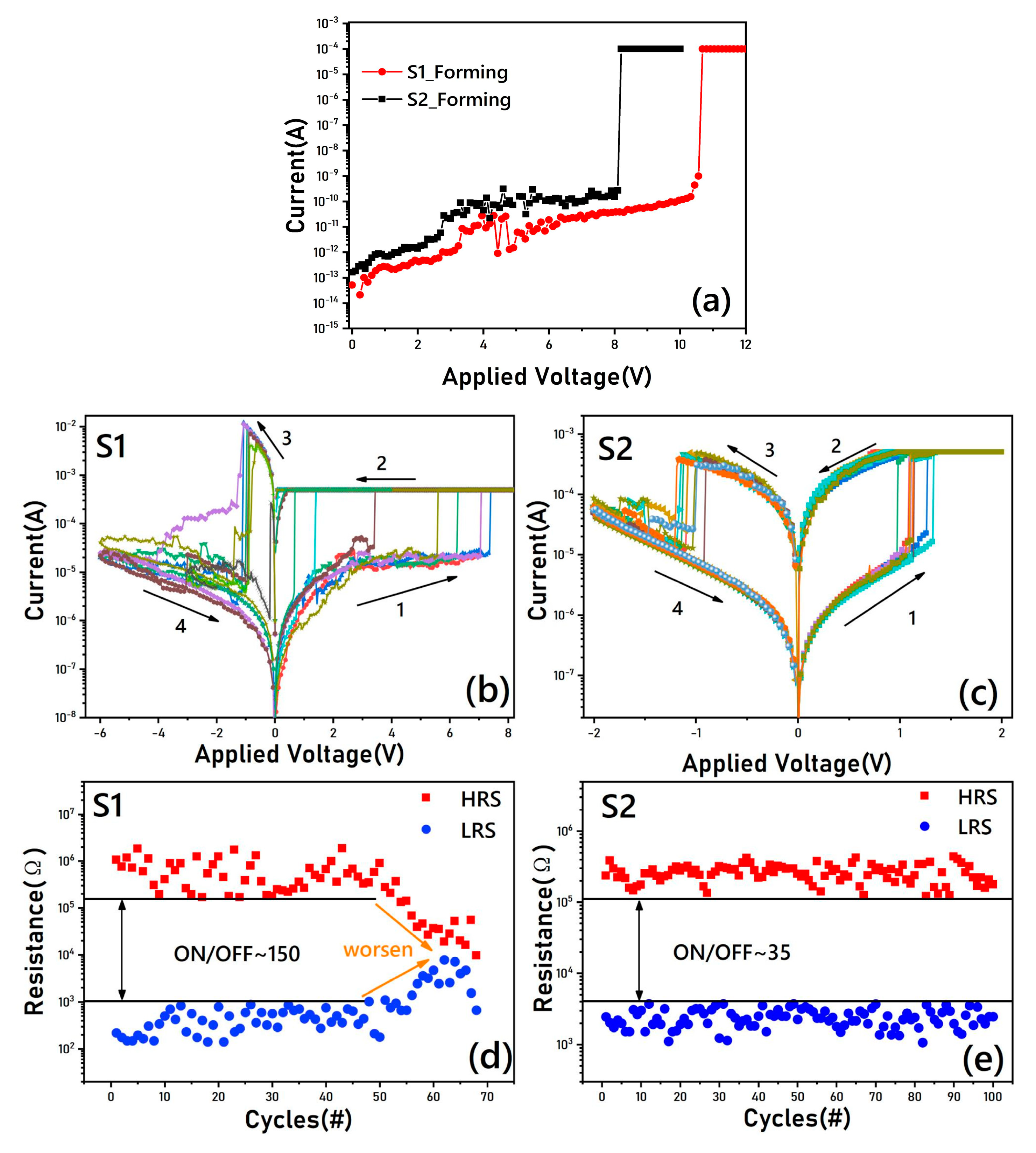
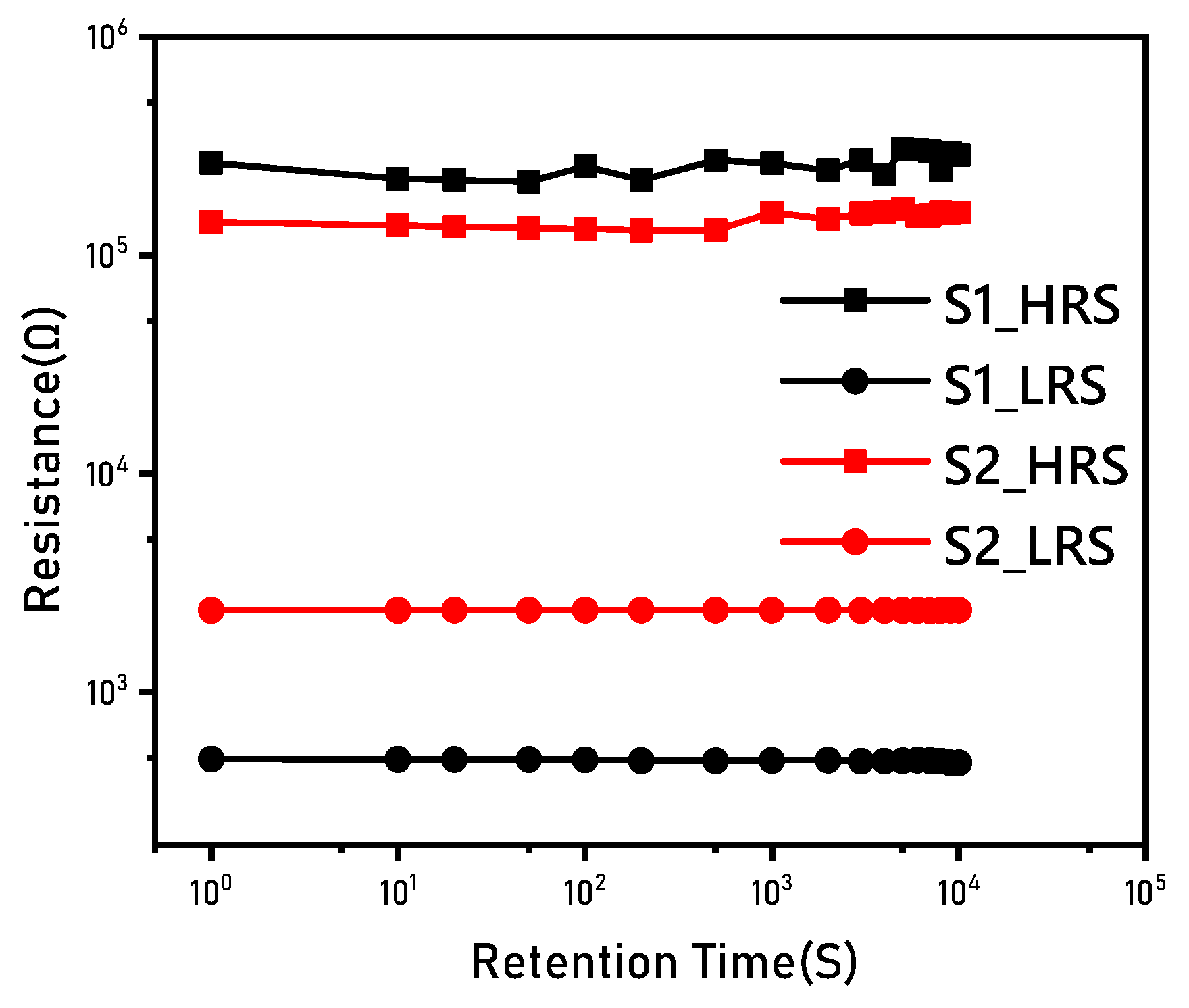
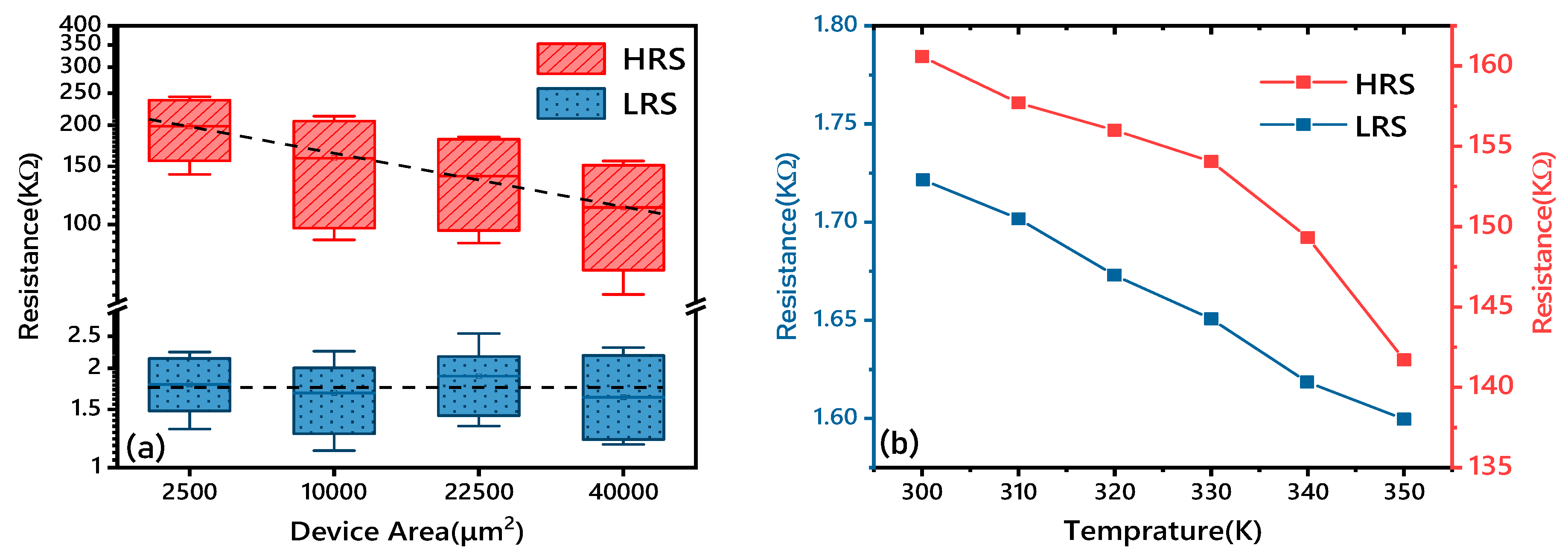
3.3. Electrical Characteristic of the RRAM Devices

Figure 4a shows the I-V characteristic curves of the devices’ forming process in S1 and S2 with a specification of 50 × 50 μm with current limiting set at 0.1 mA (stop applying voltage at 0.1 mA) to avoid device burning out due to excessive instantaneous power. S1: ITO/Al2O3/ITO devices have a large forming voltage (about 10.5 V). It can be seen that the forming voltage of S2: ITO/LaAlO3/ITO devices drops from 10.5 V to 8 V after lanthanum oxide doping. The lower operating voltage is conducive to reducing its operating power consumption and reducing the risk of circuit damage. Due to the high density and good homogeneity of the alumina dielectric film grown by ALD technology, the electric field intensity of RS layer needs to reach 5.5 MV/cm before breakdown can occur. The forming voltage of the S2: ITO/LaAlO3/ITO devices was greatly reduced (~8 V), and the electric field in the medium was around 4 MV/cm. This shows that the insertion of lanthanum oxide layer can effectively reduce the forming voltage of the devices. This may be due to the introduction of lanthanum doped impurities and defects in the medium to affect the dielectric film insulation performance, resulting in the enhancement of local electric field in the RS layer.
Figure 4b,c shows the typical current–voltage curves of DC sweep cycles for the transparent RRAM devices. It can be seen that during the SET process, the current in S1 has large fluctuations. This phenomenon can be explained as the incomplete fracture of the conductive filament during the RESET process from the perspective of the formation/fracture of the conductive filament. In the positive SET process, the current mainly never passes through the fault. At this time, a large amount of joule heat will be generated locally, and a large amount of heat will accumulate in a very short time, making the unbroken filament fuse [30]. Therefore, abnormal current rise and fall occurs. During the RESET process of the S1 RRAM devices, the current peak value of the device reached about 10 mA. The power consumption was about 10 mW. After inserting the lanthanum oxide layer in the resistive switching layer, the I-V cycle process of the S2 RRAM devices shows a more stable current, and the peak current of the device during the RESET process is only 0.5 mA, and the maximum power consumption is only about 0.5 mW, which is only equivalent to 1/20 of the power consumption of S1. In addition, the durability and operating voltage distribution of the device after doping with lanthanum have been improved to a certain extent, and the details will be shown later. Figure 4d,e shows the resistance values of the first 70 cycles of the S1 RRAM devices and the first 100 cycles of the S2 RRAM devices. The resistance of the HRS and LRS were obtained at +0.2 V, following Setting (S1:+7 V/S2:+2 V) and Resetting (S1:−4 V/S2:−2.5 V) for 30 ms. The resistance value of S1 shows a large dispersion and the window value has obviously deteriorated after about 45 cycles. The resistance may appear from 100 K ohm to 5 M ohm, and its low resistance value fluctuates between 100 Ω and 1000 Ω. Although the device switching ratio of the S2 sample is about 35 times, which is lower than the 150 times of the S1 sample, the distribution of the resistance value is more concentrated, and the cycle number of the device has been greatly improved, which has greater applications potential.
Data retention is an important indicator to measure the performance of memory devices. Figure 5 shows the retention characteristics of S1 and S2 devices at room temperature for 10,000 s. After the devices are placed in a high-resistance state/low-resistance state, the voltage and current applied to the devices are read at regular intervals and their resistance values are calculated. It can be seen from the figure that the device can maintain a stable resistance at room temperature, and its resistance hardly changes within 104 s. Therefore, S1 and S2 RRAM devices have good retention characteristics and can adapt to non-volatile memory.
As a non-volatile memory, the operating voltage distribution of RRAM devices also needs to be as concentrated as possible. In order to analyze the devices more comprehensively, 20 samples with the same size of 50 μm * 50 μm were selected from S1 and S2 respectively, and the distribution of operating voltage was statistically analyzed after multiple resistive switching cycles. Figure 6a shows the result. It can be found that the Vforming, Vset, and Vreset of S1 RRAM devices have greater dispersion. To show the difference more concretely, Figure 6b shows the cumulative probability distribution of the SET/RESET voltage of two typical samples. It can be seen that the probability distributions of S1 and S2 are quite different. Among them, the voltage distribution of S1 RRAM devices is obviously more scattered, and the SET voltage is distributed from 1 to 8 V, while the voltage distribution of S2 group is much more concentrated. In order to further analyze the voltage distribution of the devices, the voltage during the measurement process was counted, and the average value μ and standard deviation δ of Vset and Vreset of S1 and S2 were calculated, respectively. It can be seen that, after doping with lanthanum oxide, the average value of Vset decreased from 2.20 to 1.05, and the standard deviation decreased to 0.22, which was only 1/5 of the standard deviation of S1; the average value of Vreset changed from −1.04 to −0.94, and its absolute value decreased. Vreset standard deviation decreased from 0.58 to 0.13, which is only 22% of S1′s standard deviation. It shows that this method of doping lanthanum oxide effectively improves the dispersion of the operating voltage of the device and reduces the randomness in the formation of conductive filaments.

3.4. Conduction Mechanism Analysis of the RRAM Devices

Devices with four areas of 50 μm × 50 μm, 100 μm × 100 μm, 150 μm × 150 μm, and 200 μm × 200 μm were fabricated. In order to study the conductive mechanism of ITO/LaAlO3/ITO devices, 5 samples of devices of each area were taken and carried out for several resistive switching cycles, the resistance of HRS (high-resistance state) and LRS(low-resistance state) were statistically analyzed and shown in Figure 7a. It can be seen from the figure that the resistance of the LRS of the device has nothing to do with the area, while the resistance of the HRS of the device decreases as the area increases. The above phenomenon reflects that the devices are based on conductive filaments. In the HRS, the resistance of the device is mainly determined by the leakage current of the dielectric layer, so it is related to the area, while the resistance is not completely linear with the area because the RS layer conductive filaments are not completely broken during the reset process; in the LRS, the resistance value is mainly determined by the local conductive filaments, so the change of area does not affect the resistance value of the device.
Figure 7b shows the resistance of the device in the high-resistance state and the low-resistance state with temperature. Place the RRAM devices in a high-resistance state (or a low-resistance state) at room temperature, and then test the resistance value of the device under a hot plate temperature of 300–350 K to obtain the resistance–temperature relationship shown in the figure below. For resistive switching devices based on the theory of conductive filaments, the conductive filaments generally have two possible configurations: metal or oxygen vacancies. The device exhibits a semiconductor-type resistance-temperature relationship in both high resistance and low resistance states; that is, the temperature increases, and the resistance decreases. Therefore, the conductive filaments in the resistive switching device are formed by oxygen vacancies. The resistance–temperature test results strongly prove that the resistive switching device is a kind of resistive switching device based on oxygen vacancy conductive filament.
The devices use metal oxide as its electrode and RS layer, and there are many forms of conduction mechanism in it, such as ohmic transmission, space charge limited current effect trap level charge release and capture, Schottky emission effect, etc. [31]. In order to explore the mechanism of resistive switching and conduction of RRAM devices, I-V curves were fitted for different conduction mechanisms.
According to Figure 8a,b, it can be seen that the I–V characteristic curve can be divided into three regions in the high resistance state during the SET process. When the voltage is less than 0.3 V, the slope of the curve is about 0.98, which can be considered as an ohmic conduction mechanism; during the 0.3 to 0.9 V voltage scan, the slope of the curve is about 1.93, which conforms to the child’s law of conduction; in the range of 1–1.2 V, the slope of the curve is about 2.94. As the voltage increases, the current increases rapidly until it transforms into a low resistance state. During the reset process, the device also exhibits similar conduction behavior, which shows that the conduction mechanism of the RRAM device conforms to the trap-controlled space charge limited current (SCLC) conduction model [32]. Figure 8c,d shows the fitting analysis of Schottky emission and Poole-Frenkel emission. It can be found that there is a linear relationship between ln(I) and V0.5 of ITO/LaAlO3/ITO RRAM devices at about 0.4 V–1.0 V, indicating that the device also conforms to the Schottky barrier conduction mechanism in this voltage range.
Figure 9 shows the resistance switching process based on the conductive filament theory. As the voltage increases, the oxygen ions in the LaAlO3 resistive switching film and the ITO bottom electrode migrate to the RS layer/top electrode interface, reducing the Schottky barrier at the interface, and at the same time generating oxygen vacancies in the RS layer. At this stage, the electron transmission of the device is dominated by Schottky emission, the Schottky barrier at the RS layer/top electrode is reduced with the resistance of the device. Conversely, when a negative bias is applied, oxygen ions migrate to the bottom electrode, and the Schottky barrier at the interface increases with the increase in device resistance [33].
Based on the above analysis, when the applied voltage is very small, the conductive mechanism of the device is dominated by ohmic transmission. As the voltage rises, the oxygen ions in the RS layer migrate and form oxygen vacancies, which in turn affects the Schottky barrier height at the interface and causes the device resistance to change. As the voltage continues to rise, conductive filaments formed in the LaAlO3 film connect the top electrode and the bottom electrode, and the RRAM device changes to a low resistance state. At this time, the electron transport mechanism of the device changes to ohmic contact. On the contrary, when a negative bias is applied, oxygen ions migrate to the bottom electrode, the Schottky barrier at the interface increases, and the device resistance increases [34].

4. Conclusions

In summary, in the work of this article, high-transparency ITO/LaAlO3/ITO RRAM devices were successfully fabricated on glass substrates. The performance of the devices is effectively improved by inserting LaOx layer during the fabrication of the RS layer by ALD equipment. The fabricated TRRAM has a light transmittance of about 75% in the visible light range, has a stable operating voltage distribution, a switching ratio of about 40 times, and a retention time of up to 10,000 s. The light transmittance of the RS layer is as high as 95%. The resistive switching mechanism of the device is mainly controlled by the SCLC mechanism, supplemented by the Schottky emission principle, and the resistive switching is completed by the formation and rupture of oxygen vacancy filaments. The work of this paper presents the huge application potential of lanthanum-based rare earth oxide as a resistive switching layer in the field of transparent RRAM.

Author Contributions

G.H. designed the experiment, completed the experiment, wrote the manuscript; Y.C. and H.L. provided funding support and resources; D.W. supervised the study; R.Q. managed the project. All authors have read and agreed to the published version of the manuscript.

Funding

This research was supported by the National Natural Science Foundation of China (Grant No. U1866212), the Laboratory Open Fund of Beijing Smart-chip Microelectronics Technology Co., Ltd. (Grant No. SGITZXDDKJQT2002303).

Conflicts of Interest

The authors declare no conflict of interest.

References

  1. Chen, Z.; Huang, W.; Zhao, W.; Hou, C.; Ma, C.; Liu, C.; Sun, H.; Yin, Y.; Li, X. Nonvolatile memory: Ultrafast multilevel switching in Au/YIG/n-Si RRAM. Adv. Electron. Mater. 2019, 5, 1800418. [Google Scholar] [CrossRef]
  2. He, Z.-Y.; Wang, T.-Y.; Chen, L.; Zhu, H.; Sun, Q.-Q.; Ding, S.-J.; Zhang, D.W. Atomic layer-deposited HfAlOx-based RRAM with low operating voltage for computing in-memory applications. Nanoscale Res. Lett. 2019, 14, 51. [Google Scholar] [CrossRef] [Green Version]
  3. Xu, W.; Zhao, Y.; Huang, P.; Liu, X.; Kang, J. 3D vertical RRAM array and device co-design with physics-based spice model. In Proceedings of the 2019 IEEE 13th International Conference on ASIC (ASICON), Chongqing, China, 29 October–1 November 2019; IEEE: Piscataway, NJ, USA, 2019; pp. 1–4. [Google Scholar]
  4. Zayer, F.; Lahbacha, K.; Dghais, W.; Belgacem, H.; De Magistris, M.; Melnikov, A.V.; Maffucci, A. Electrothermal analysis of 3D memristive 1D-1RRAM crossbar with carbon nanotube electrodes. In Proceedings of the 2019 IEEE International Conference on Design & Test of Integrated Micro & Nano-Systems (DTS), Gammarth-Tunis, Tunisia, 28 April–1 May 2019; IEEE: Piscataway, NJ, USA, 2019; pp. 1–6. [Google Scholar]
  5. Shrestha, P.R. Fast transients in non-volatile resistive memories (RRAM) using tantalum pentoxide as solid electrolyte. In Dissertations and Theses Gradworks; Old Dominion University: Norfolk, VA, USA, 2013; pp. 2549–2554. [Google Scholar]
  6. Zhang, W.; Hu, Y.; Chang, T.-C.; Chang, K.-C.; Tsai, T.-M.; Chen, H.-L.; Su, Y.-T.; Chu, T.-J.; Chen, M.-C.; Huang, H.-C.; et al. An electronic synapse device based on solid electrolyte resistive random access memory. IEEE Electron. Device Lett. 2015, 36, 772–774. [Google Scholar] [CrossRef]
  7. Ram, M.S.; Persson, K.-M.; Borg, M.; Wernersson, L.-E. Low-power resistive memory integrated on III–V vertical nanowire MOSFETs on silicon. IEEE Electron. Device Lett. 2020, 41, 1432–1435. [Google Scholar] [CrossRef]
  8. Persson, K.A.; Ram, M.S.; Kilpi, O.E.; Borg, M.; Wernersson, L. Cross-point arrays with low power ITO/HfO2 resistive memory cells integrated on vertical nanowires. Adv. Electron. Mater. 2020, 6, 2000154. [Google Scholar] [CrossRef]
  9. Wu, S.-J.; Wang, F.; Zhang, Z.-C.; Li, Y.; Han, Y.-M.; Yang, Z.-C.; Zhao, J.-S.; Zhang, K.-L. High uniformity and forming-free ZnO-based transparent RRAM with HfOx inserting layer. Chin. Phys. B 2018, 27, 087701. [Google Scholar] [CrossRef]
  10. Salaoru, I.; Prodromakis, T.; Khiat, A.; Toumazou, C. Resistive switching of oxygen enhanced TiO2 thin-film devices. Appl. Phys. Lett. 2013, 102, 013506. [Google Scholar] [CrossRef]
  11. Ismail, M.; Rana, A.M.; Talib, I.; Tsai, T.-L.; Chand, U.; Ahmed, E.; Nadeem, M.Y.; Aziz, A.; Shah, N.A.; Hussain, M. Room-temperature fabricated, fully transparent resistive memory based on ITO/CeO2/ITO structure for RRAM applications. Solid State Commun. 2015, 202, 28–34. [Google Scholar] [CrossRef]
  12. Liu, L.N.; Tang, W.M.; Lai, P.-T. Advances in la-based high-k dielectrics for MOS applications. Coatings 2019, 9, 217. [Google Scholar] [CrossRef] [Green Version]
  13. Jin-shun, B.; Zheng-sheng, H. Study on Hf/HfO2 bipolar resistive random-access-memory. J. Funct. Mater. Devices 2014, 5, 002. [Google Scholar]
  14. Yu, W.; Li, X.; Rui, Y.; Liu, X.; Wang, Q.; Chen, L. Improvement of resistive switching property in a noncrystalline and low-resistance La0.7Ca0.3MnO3 thin film by using an Ag–Al alloy electrode. J. Phys. D Appl. Phys. 2008, 41, 215409. [Google Scholar] [CrossRef]
  15. Wang, Y.; Liu, H.; Wang, X.; Zhao, L. Impacts of Cu-doping on the performance of La-based RRAM devices. Nanoscale Res. Lett. 2019, 14, 1–9. [Google Scholar] [CrossRef] [PubMed]
  16. Kim, S.M.; Kim, H.J.; Jung, H.J.; Park, J.Y.; Seok, T.J.; Choa, Y.H.; Park, T.J.; Lee, S.W. High-performance, transparent thin film hydrogen gas sensor using 2D electron gas at interface of oxide thin film heterostructure grown by atomic layer deposition. Adv. Funct. Mater. 2019, 29, 1807760.1–1807760.8. [Google Scholar] [CrossRef]
  17. Leskelä, M.; Ritala, M. Atomic layer deposition (ALD): From precursors to thin film structures. Thin Solid Films 2002, 409, 138–146. [Google Scholar] [CrossRef]
  18. Wang, Y.; Liu, H.; Wang, X.; Zhao, L. Impact of remote oxygen scavenging on the interfacial characteristics of atomic layer deposited LaAlO3. Mater. Sci. Semicond. Process. 2019, 90, 50–53. [Google Scholar] [CrossRef]
  19. Liu, H.; Wang, X. Impact of Al+ implantation on the Switching Characteristics of Al2O3/La2O3/Al2O3 multilayer RRAM devicesevices. In Proceedings of the International Conference on IC Design and Technology, Suzhou, China, 17 June–19 June 2019; IEEE: Piscataway, NJ, USA, 2019; pp. 1–4. [Google Scholar]
  20. Calnan, S.; Tiwari, A.N. High mobility transparent conducting oxides for thin film solar cells. Thin Solid Films 2010, 518, 1839–1849. [Google Scholar] [CrossRef]
  21. Wu, J.; Becerril, H.A.; Bao, Z.; Liu, Z.; Chen, Y.; Peumans, P. Organic solar cells with solution-processed graphene transparent electrodes. Appl. Phys. Lett. 2008, 92, 263302. [Google Scholar] [CrossRef] [Green Version]
  22. Pan, J.; Li, S.; Ou, W.; Liu, Y.; Li, C. The photovoltaic conversion enhancement of NiO/Tm:CeO2/SnO2 transparent p-n junction device with dual-functional Tm:CeO2 quantum dots. Chem. Eng. J. 2020, 393, 124802. [Google Scholar] [CrossRef]
  23. Suh, S.; Yi, K.; Choi, C.; Park, D.; Kim, C. Mobile LCD device with transparent infrared image sensor panel for touch and hover sensing. In Proceedings of the 2012 IEEE International Conference on Consumer Electronics (ICCE), Las Vegas, CA, USA, 12–15 January 2012; IEEE: Piscataway, NJ, USA, 2012; pp. 213–214. [Google Scholar]
  24. Zhang, T.; Ou, X.; Zhang, W.; Yin, J.; Xia, Y.; Liu, Z. High-k-rare-earth-oxide Eu2O3 films for transparent resistive random access memory (RRAM) devices. J. Phys. D Appl. Phys. 2014, 47, 162–172. [Google Scholar] [CrossRef]
  25. Chen, K.H.; Tsai, T.M.; Cheng, C.M.; Huang, S.J.; Young, T.F. Schottky emission distance and barrier height properties of bipolar switching Gd:SiOx RRAM devices under different oxygen concentration environments. Materials 2018, 11, 43. [Google Scholar] [CrossRef] [Green Version]
  26. Chen, C.Y.; Goux, L.; Fantini, A.; Redolfi, A.; Groeseneken, G.; Jurczak, M. Low-current operation of novel Gd2O3 -based RRAM cells with large memory window. Phys. Status Solidi (A) 2015, 213, 320–324. [Google Scholar] [CrossRef]
  27. Ali, K.; Choi, K.H.; Jo, J.; Lee, Y.W. High rate roll-to-roll atmospheric atomic layer deposition of Al2O3 thin films towards gas diffusion barriers on polymers. Mater. Lett. 2014, 136, 90–94. [Google Scholar] [CrossRef]
  28. Martin, W.C.; Wiese, W.L.; Musgrove, A.; Fuhr, J.R.; Sugar, J.; Reader, J.; Kelleher, D.E.; Olsen, K.J.; Mohr, P.J.; Dalton, G.R. NIST atomic spectra database. Mem. Soc. Astron. Ital. Suppl. 2005, 8, 96. [Google Scholar]
  29. Lee, B.; Park, T.; Hande, A.; Kim, M.; Wallace, R.M.; Kim, J.; Liu, X.; Yi, J.; Li, H.; Rousseau, M.; et al. Electrical properties of atomic-layer-deposited La2O3 films using a novel La formamidinate precursor and ozone. Microelectron. Eng. 2009, 86, 1658–1661. [Google Scholar] [CrossRef]
  30. Seo, J.W.; Park, J.-W.; Lim, K.S.; Yang, J.-H.; Kang, S.J. Transparent resistive random access memory and its characteristics for nonvolatile resistive switching. Appl. Phys. Lett. 2008, 93, 223505. [Google Scholar] [CrossRef]
  31. Lee, J.; Schell, W.; Zhu, X.; Kioupakis, E.; Wei, D.L. Charge transition of oxygen vacancies during resistive switching in oxide-based RRAM. Acs Appl. Mater. Interfaces 2019, 11, 11579–11586. [Google Scholar] [CrossRef]
  32. Hsu, S.T.; Li, T. RRAM electronics and switching mechanism. MRS Proc. 2007, 997, 0997. [Google Scholar] [CrossRef]
  33. Szot, K.; Speier, W.; Bihlmayer, G.; Waser, R. Switching the electrical resistance of individual dislocations in single-crystalline SrTiO3. Nat. Mater. 2006, 5, 312–320. [Google Scholar] [CrossRef]
  34. Piros, E.; Petzold, S.; Zintler, A.; Kaiser, N.; Vogel, T.; Eilhardt, R.; Wenger, C.; Molina-Luna, L.; Alff, L. Enhanced thermal stability of yttrium oxide-based RRAM devices with inhomogeneous Schottky-barrier. Appl. Phys. Lett. 2020, 117, 013504. [Google Scholar] [CrossRef]
Figure 1. Schematic diagram of devices fabrication process.
Electronics 10 00272 g001
Figure 2. (a) Full spectrum of XPS test; (b) The 1s peak spectrum of O element; (c) The 3d peak spectra of the La element; (d) 2p peak spectrum of Al element.
Electronics 10 00272 g002
Figure 3. Wavelength—Transmittance diagram of RRAM.
Electronics 10 00272 g003
Figure 4. (a) The I-V diagram of the RRAM devices’ forming process; (b) I-V cycling characteristics of S1:ITO/Al2O3/ITO RRAM with ICOMP = 0.5 mA; (c) I-V cycling characteristics of S2:ITO/LaAlO3/ITO RRAM with ICOMP = 0.5 mA; (d) Endurance test of S1 RRAM devices; (e) Endurance test of S2 RRAM devices.
Electronics 10 00272 g004
Figure 5. Data retention time of S1 and S2 RRAM devices.
Electronics 10 00272 g005
Figure 6. (a) Operating voltage distribution of RRAM devices; (b) Cumulative probability of SET/RESET voltages.
Electronics 10 00272 g006
Figure 7. (a) Area dependence of resistance; (b)Temperature dependence of resistance.
Electronics 10 00272 g007
Figure 8. (a) Double logarithmic plotting of set process; (b) Double logarithmic plotting reset process (c) Ln(I)–V0.5 plotting of the set process; (d) Ln(I/V)–V0.5 plotting of the set process.
Electronics 10 00272 g008
Figure 9. Schematic diagram of resistance switching process of RRAM devices.
Electronics 10 00272 g009
Table 1. Single cycle growth parameters of ALD.
La2O3Al2O3
PulseTimePulseTime
La(i-PrCp)30.1 sAl(CH3)3 0.1 s
N24 sN2 3 s
O30.3 sO30.5 s
N210 sN2 4 s
Publisher’s Note: MDPI stays neutral with regard to jurisdictional claims in published maps and institutional affiliations.

