1. Introduction
The power electronics field is related to the electrical energy transformation through electronic components; one of their specific fields is the development of large voltage gain dc–dc converters [
1], which are important in renewable energy generation systems and other environmentally friendly applications [
2], for example, in photovoltaic (PV) panels or fuel cells (FCs), in which the dc voltage that comes from the PV panel or the FC, must be increased from some dozens of volts to some hundreds of volts.
There are traditional topologies, such as the buck, boost, or buck–boost converter, some of them has the capability to increase the input voltage, but the required voltage gain can be too large for traditional topologies [
3], manufacturers of integrated circuits for the control of power converters, usually do not warranty their circuits can work with duty cycles larger than 0.75 or 0.8, which would limit the operation of traditional converters to voltage-gains of around five [
3] (the definition of duty cycle and their relation to voltage gain will be further explained).
A solution to achieve a large voltage gain is the use of transformers or coupled inductors [
1], but transformer-less converters can be manufactured with available commercial components (off-the-shelves), which make them attractive, while magnetic-coupling based converters, based for example on transformers or coupled inductors, usually require the magnetic component to be designed in a custom manner. On the other hand, the magnetic coupling may provide electrical isolation to the converter. If electrical isolation is not required, transformer-less topologies are cheaper, and their manufacturing process is faster.
Other solutions to achieve large voltage gain are the use of voltage multipliers combined with traditional converters [
4,
5,
6], or quadratic topologies [
7,
8].
Additionally, then, the research on transformer-less topologies is an active field. One of the recently investigated transformer-less dc–dc boost converter topologies is the so-called, multistage-stacked boost architecture (MSBA) converter, initially introduced in [
9,
10], has been studied in other works of the literature; for example, their control has been studied in [
11]. In contrast to other large voltage gain topologies, such as other quadratic topologies, the MSBA converter allows one to increase the structure and attain voltage levels that are higher than the blocking capability of the semiconductor devices [
9], their structure can be extended with similar building blocks. On the other hand, it has two transistors in contrast to other dc–dc converters, which utilizes a single switch; furthermore, if the structure is extended, more transistors are required.
This article analyzes the operation mode of the multistage-stacked boost architecture MSBA converter working under symmetric operation mode, and it proposes a new operation mode with a modified pulse width modulation (PWM) scheme. In the modified PWM scheme, the switching functions of transistors are obtained from an interleaved PWM and shifted 180°. The interleaved PWM has been utilized in several studies to reduces the input current ripple in converters [
12]; this work is focused on the output voltage ripple.
The results show that the modified PWM results in a similar operation of the converter; it has the same equilibrium and the same power rating in all devices, but it offers a reduction on the output voltage ripple without increasing the switching frequency; if the switching frequency can be increased, the designer still can choose the proposed strategy and achieve a smaller voltage ripple compared to the former strategy. A mathematical model of the converter is provided, the output voltage ripple calculation is performed in the traditional, and the modified PWM scheme, simulation, and experimental results are provided to verify the operation mode and the obtained equations.
2. The MSBA Converter with Non-Interleaved PWM
The topology understudy is depicted in
Figure 1. It is composed of two inductors
L1 and
L2, two capacitors
C1 and
C2, two transistors
s1 and
s2, and two diodes
s1n and
s2n. Diodes switch complementary with transistors; when a transistor is closed, their complementary diode is open, and vice-versa; the subtitle “
n” (from “
not”) in the name of diodes indicates their complementary transistor,
s1n is complementary to
s1, and
s2n is complementary to
s2.
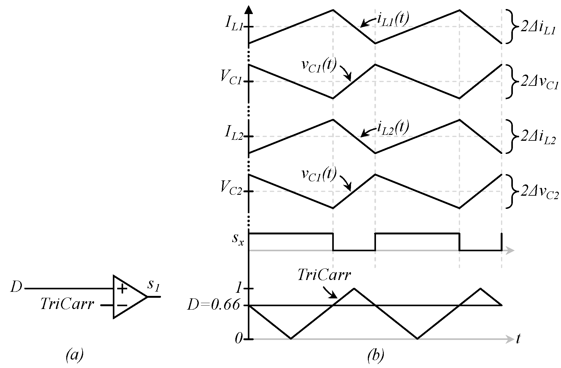
In the symmetric operation mode, both transistors share the same switching function
sx and duty cycle
D;
Figure 2a shows the block diagram of the pulse width modulation (PWM) scheme at the former operation mode of the converter, and
Figure 2b shows important waveforms in this process, the first four signals are the state variables of the converter, the current through both inductors and the voltage across capacitors’ terminals. At the button of
Figure 2b, the switching function
sx is shown over the triangular carrier and the duty cycle signal, which are depicted together at the button of the figure.
The switching function sx, also called the PWM signal, is obtained by comparing the dc signal “D” (which can take values between 0 and 1) against a triangular carrier TriCarr. The switching function sx = 1 when D is larger than TriCarr, and sx = 0 when D is below the signal TriCarr.
The operation of the converter produces two different switching states or equivalent circuits,
Figure 3a shows the equivalent circuit of the converter when
sx = 1, both transistors are closed, and diodes are reversely polarized (
s1n whit
VC1 and
s2n with
VC1 +
VC2).
Those switching states lead to two different mathematical models; by following the Kirchhoff voltage law (KVL) and the Kirchhoff current law (KCL), the mathematical model of the circuit shown in
Figure 3a is given by (1) and (2).
Being C1 and C2 the capacitance of their respective capacitors; L1 and L2 the inductance of inductors; vC1 and vC2 the voltage across capacitors C1 and C2; iL1 and iL2 the currents through inductors L1 and L2; vg is the input voltage; and io is the output current, the current through the output resistor, which in this case is equal to (vC1 + vC2)/R.
The mathematical model of the circuit shown in
Figure 3b is given by (3) and (4).
Now the traditional averaging technique [
1] can be used to determine the full average model. However, first, let’s remind that the duty cycle
D is defined as the relation of the time period in which a transistor is closed, divided over the total switching period
TS. The remainder of the average time (in which the transistor is open) can be expressed as (1 −
D). From this definition, the time period in which the circuit behaves like
Figure 3a is equal to
DTS, and the time in which the circuit behaves like
Figure 3b is equal to (1 −
D)
TS. In order to obtain the average model, the value of variables in each switching state can be multiplied by the time each switching state holds and divided over the total switching period
TS. This leads to:
The term
TS is not present since it is canceled during the averaging process; furthermore, the lowercase “
d” is used instead of the uppercase “
D”, in general, lowercase letters are used to indicate that signals can change (are variables), and uppercase letters are used to indicate they operate in steady-state (considered as constant in this specific condition). The average model in (5)–(8) can be further simplified to the model in (9)–(12).
The mathematical model described in (9)–(12) is sometimes called the non-linear, or full average, or large-signal model of the converter; from this large-signal model, the steady-state condition or equilibrium can be obtained when derivatives are equal to zero, the equilibrium is calculated (13) and (14).
Finally, the output voltage of the converter, see
Figure 1, is given by the series connection of both capacitors, the output voltage is then the summation of
VC1 +
VC2, and finally expressed in terms of the input voltage
Vg and the duty cycle
D as (15).
The equilibrium described in (13) and (14) is similar to the equilibrium of the classical quadratic boost converter. The discussed converter is also a quadratic boost, which can be observed from their output voltage (15). One advantage of the MSBA converter against the quadratic boost is that capacitor C2 has less voltage rating, which has an impact on the size of the converter; on the other hand, it requires two transistors, while the traditional quadratic boost requires only one.
The Output Voltage Ripple
The output voltage ripple is an important parameter to define the power quality of the converter; it is desired to have an output voltage as pure (or clean) as possible, which means as free of switching ripple as possible. A pure DC signal would be desirable, but this is impossible; it would require an infinitely large capacitance. The output voltage ripple can be reduced by choosing larger capacitors, but this brings a compromise between the size of the converter and the output voltage ripple.
As described ahead, the MSBA converter can offer an advantage in this matter when it is operated with the modified PWM scheme, but first, the traditional operation mode is described to have a comparison point.
The voltage ripple in each capacitor can be calculated considering that their voltage decreases when then transistors are closed; since their current is negative in this particular switching state, this lasts for a time period equal to
DTS. The derivative of the voltage or voltage slope in a capacitor is equal to their current divided over the capacitance
dv/dt = I/C. Considering that the voltage ripple in
C1 and
C2 can be calculated as:
The ripple is an absolute value, and then the current through the capacitor can be expressed as positive; the number 2 comes from the fact that the ripple is defined as the maximum deviation from the average voltage; the average is at the middle point in the triangular waveform. Peak to peak variation in
Figure 2 is labeled as twice of the ripple.
Similarly to the switching ripple in capacitors voltage, there is a switching ripple in inductors currents, and they can be similarly calculated [
1]; this article focuses on the voltage ripple.
From
Figure 2, the ripples in capacitors are in phase, the voltage in capacitors rise and fall at the same time, capacitors are connected in additive series, which produces that the output voltage ripple is the summation of the ripple in individual capacitors.
3. The MSBA Converter in the Proposed Operation Mode
The proposed operation mode of the MSBA converter is based on an interleaved PWM scheme, and shown in
Figure 4, like the PWM scheme in interleaved converters, there is a single duty cycle signal, but two triangular carriers shifted 180°, called in this case
s1Carr and
s2Carr switching functions of transistors are different, but they have the same duty cycle (the same proportion of time in the closed position of the switch).
The proposed operation mode is more complex to analyze than the former operation mode for the following reason, in the former operation mode, there were two transistors operating with the same switching functions; this produces only two switching states, or equivalent circuits, as shown in
Figure 3. Having only two switching states simplifies the averaging process. However, if each transistor has their own switching function, there are four possible switching states, which are shown in
Figure 5, those switching states are: (i)
s1 = 1 and
s2 = 0, (ii)
s1 = 0 and
s2 = 1, (iii)
s1 = 1 and
s2 = 1, and (iv)
s1 = 0 and
s2 = 0.
Even if the number of possible switching states is four, the number of switching states that appears during the operation mode is three (two in a particular point), and they depend on the value of the duty cycle
D. The duty cycle
D may change during the operation, adjusted by a controller (for example, a PID controller), to maintain the output voltage in a certain desired value. The operation of the converter can be classified in three possible cases (when
D < 0.5,
D = 0.5, and
D > 0.66).
Figure 6 shows three particular cases (when
D = 0.33,
D = 0.5, and
D = 0.66) to exemplify how switching functions would look like and to observe how the different equivalent circuits may appear.
Case
D < 0.5: When the duty cycle is smaller than 0.5, PWM signals are as shown in
Figure 6a; the low value of
D causes each switch to close for a short period of time, and the second transistor to close after a time in which both signals are off (a digital 0). There is not a time in which both transistors are closed at the same time (signals blue and gray are not high simultaneously in
Figure 6a, and then the switching state in
Figure 5c did not appear, all other three switching states in
Figure 5 (
s1 = 1 and
s2 = 0,
s1 = 0 and
s2 = 1, and
s1 = 0 and
s2 = 0) are present in this operation mode.
Case
D = 0.5: In this particular case, only two switching states are present, see
Figure 6b; those switching states are when transistors are
s1 = 1 and
s2 = 0, and
s1 = 0 and
s2 = 1 (see
Figure 5a,b). This particular case can be analyzed as any of the other two cases in their boundary case.
Case
D > 0.5: This operation mode is shown in
Figure 6c, which in contrast to other diagrams in
Figure 6, the time calculations for the different periods are also shown; this is because this operation mode is the focus of this article. In this operation mode, there is not a time in which both transistors are open at the same time, but there is a time in which both transistors are closed at the same time. The switching states that appear during this operation mode are
s1 = 1 and
s2 = 0,
s1 = 0 and
s2 = 1, and
s1 = 1 and
s2 = 1.
Despite the four possible combinations of switch positions, the proposed operation mode does not affect the mathematical model; at the end of the averaging, the mathematical model of the converter is still described by Equations (9)–(12). That means the proposed operation provides the same dynamic performance to the MSBA converter, compared to the former strategy. The equilibrium is also described as (13) and (14). Equations are not repeated for convenience. The difference is the calculation of the output voltage ripple, which is certainly different to (17).
The Output Voltage Ripple in the Proposed Operation Mode
Before providing the equations to calculate the output voltage ripple in the proposed operation mode, a discussion about the ripple origin may improve the understanding of the principle.
In the former operation mode, during any of both switching states (see
Figure 3), both capacitors are getting charged or discharged at the same time. In
Figure 3a, capacitor
C1 is getting discharged with
IL2 +
Io, while capacitor
C2 is getting discharged with
Io; both capacitors (which are series-connected) are getting discharged at the same time. On the other hand, in
Figure 3b, capacitor
C1 is getting charged with
IL1 −
Io (is getting charged since
Io is smaller than
iL1 as stated in (14)), while capacitor
C2 is getting charged with
IL2 −
Io (is getting charged since
Io is smaller than
iL2 as stated in (14)). The conclusion is that both capacitors get charged or discharged at the same time, and then the ripple of individual capacitors gets a cumulative contribution to the output voltage ripple.
In the proposed operation mode, the discussed switching states are also present; notice that
Figure 3a is equal to
Figure 5c, and
Figure 3b is equal to
Figure 5d, but the other two switching state are present in which one capacitor is getting charged while the other one is getting discharged, and thus represent a non-cumulative contribution to the output voltage ripple.
In
Figure 5a, capacitor
C1 is getting discharged with
Io, while capacitor
C2 is getting charged with
IL2 −
Io. On the other hand, in
Figure 5b, capacitor
C1 is getting charged with
IL1 −
IL2 −
Io, while capacitor
C2 is getting charged with
Io. The conclusion is that in those new switching states, one capacitor gets charged while the other gets discharged, and vice-versa; this behavior helps to reduce the output voltage ripple since the ripple of individual capacitors does not get a cumulative contribution to the output voltage ripple.
To calculate the output voltage ripple in the proposed operation mode of the MSBA converter, we must consider that the maximum voltage variations (the switching ripple) can be present on one of the new switch states, the one shown in
Figure 5a, or the one shown in
Figure 5b, this depends on the duty cycle (as explained the new operation mode has two different sets of switching states (see
Figure 6). Additionally, From
Figure 6, both new switching states hold for a time (1 −
D)
TS. The expression for the output voltage ripple is then the largest value of those ripples expressed in (18) and (19), respectively.
Equations (18) and (19) will provide different values, but as will be shown in the next section, both have a smaller ripple compared to (17) for the same size of devices and power rating, without increasing the switching frequency, if the switching frequency can be larger, the designer still can choose the proposed strategy and achieve a smaller voltage ripple compared to the former strategy, the best choice would be the combination of the proposed strategy with the largest possible switching frequency (the switching frequency of the design can be limited by the semiconductors technology and the losses).
Figure 7 shows a zoom into the theoretical waveforms of the output voltage ripple;
Figure 7a shows the former strategy; only two switching states are present, the state in which both transistors are on (
Figure 5c) and the state in which both switches are off (
Figure 5d),
Figure 7 shows the derivative of the output voltage as the summation of the derivative of voltages across both capacitors, as it can be observed Equation (17) corresponds to the time in which transistors are closed, and both capacitors are getting discharged.
Figure 7b shows the zoom intro the output voltage ripple in the proposed strategy, the falling derivative is always the same, since the switching state is also the one shown in
Figure 5c, when both transistors are closed, on the other hand, the rising derivative may be produced for two different switching states, when
s1 is closed while
s2 is open (
Figure 5a), and when
s1 is open while
s2 is closed (
Figure 5b). Those two rising derivatives were used to determine (18) and (19).
4. Comparative Evaluation and Discussion
In this section, two MSBA converters with the same design are compared, with the former and the proposed operation mode; as mentioned before, the equilibrium does not change, both converters have the same power rating, but the output voltage ripple is smaller for the proposed operation mode within the full operating range. Both converters have equal inductance in inductors L1 = L2 = 330 µH; the switching frequency is selected as 50 kHz. The capacitance of capacitors was initially selected as C1 = C2 = 20 µF for both capacitors, then two additional cases with different capacitance were tested.
The comparative evaluation is based on the numerical simulation of a real application, in which an MSBA boost converter is fed with a fuel cell (FC), which voltage varies from 20 to 25 V, the output voltage is expected to be a constant 200 V dc bus, which feeds a grid-tie inverter. The power varies linearly depending on the FC parameters; the maximum voltage was attained when the minimum current was drawn from the FC, the minimum current was 2A; on the other hand, the minimum voltage was attained when the maximum current was drawn from the FC, the maximum current is 10 A. Those parameters are similar to the operation of a real FC; see FCS-C200 from [
13].
Figure 8 shows the output voltage ripple for the former operation mode and the new operation mode (both Equations (18) and (19)) vs. the input voltage; it can be observed that the proposed operation mode achieved a lower output voltage ripple for the full operating range.
Similar to
Figure 8 and
Figure 9 the output voltage ripple is shown, but in this case, the value of capacitors was different, in this case,
C1 = 20 µF while
C2 = 10 µF, the change has been done to show how the largest value of the ripple in Equations (18) and (19), depends on the duty cycle and the value of capacitors, in this case, for an input voltage smaller than 22 V, the output voltage ripple of the proposed strategy must be calculated with Equation (18), on the other hand, for an input voltage larger than 22 V, the output voltage ripple of the proposed strategy must be calculated with Equation (19), both equations must be evaluated, and the largest value must be considered as the output voltage ripple. Despite that Equations (18) and (19) provided a smaller output voltage ripple compared to the former operation mode for the entire operating range.
A particular point in
Figure 9 is marked with red circles;
Figure 10 shows the simulation results for the output voltage in this particular point. The output voltage was 200 V dc with a small ripple; the figure shows a zoom in, in which (only) 5 V are shown (from 198 to 203 V); the zoom was made to appreciate the ripple, it seemed the voltage was well regulated to 200 V, the output voltage of a converter controlled in the former strategy is shown in black color, the output voltage ripple for the proposed strategy is shown in blue, a couple of measurement shows the peak-to-peak the ripple in the DeltaY measurement. Reminder that the peak-to-peak ripple is twice of Equations (17)–(19). Values can vary in a small percentage since Matlab calculates the equations, and the Synopsys Saber simulator provides a switched simulation with all parameters of components, including losses and parasitic elements.
As another example, we could reduce the capacitance of capacitors and obtain similar (or superior) performance with smaller capacitors; the last example, shown in
Figure 11, compares the former operation mode with capacitors of
C1 = 20 µF and
C2 = 10 µF, against the proposed operation mode with capacitors of
C1 = 6.8 µF and
C2 = 3.3 µF.
Figure 11 shows that even with smaller capacitors, the proposed operation mode achieved a smaller output voltage ripple in the entire operating range.


