Article

CDM Protection Test Structure for I/O Cells in a Submicronic Technology

by
Mihaela-Daniela Dobre
1,2,*,
Philippe Coll
3 and
Gheorghe Brezeanu
2
1
Microchip Technology Inc., 061344 Bucharest, Romania
2
Faculty of Electronics, Telecommunications and Information Technology, University Polyethnic, 061071 Bucharest, Romania
3
Microchip Technology Inc., 13106 Rousset, France
*
Author to whom correspondence should be addressed.
Electronics 2021, 10(4), 443; https://doi.org/10.3390/electronics10040443
Submission received: 31 December 2020 / Revised: 28 January 2021 / Accepted: 5 February 2021 / Published: 11 February 2021
(This article belongs to the Section Circuit and Signal Processing)

Abstract

:
This paper proposes an investigation of a CDM (charge device model) electrostatic discharge (ESD) protection method used in submicronic input–output (I/O) structures. The modeling of the commonly used ESD protection devices as well as the modeling of the breakdown caused by ESD is not accurate using traditional commercial tools, hence the need for test-chip implementation, whenever a new technology node is used in production. The proposed method involves defining, implementing, testing, and concluding on one test-chip structure named generically “CDM ground resistance”. The structure assesses the maximum ground resistance allowed for the considered technology for which CDM protection is assured. The findings are important because they will be actively used as CDM protection for all I/O structures developed in the considered submicronic technology node. The paper will conclude on the constraints in terms of maximum resistance of ground metal track allowed to be CDM protected.

1. Introduction

Electrostatic discharge (ESD) is one of the main reasons for failures in integrated circuits (ICs) [1,2,3,4,5,6,7,8,9,10,11,12,13,14,15,16,17,18,19,20,21,22,23,24,25,26,27,28]. There are several models developed to describe this phenomenon: HBM (human body model), MM (machine model) and CDM (charge device model) [2]. Each of these models describe a particular type of discharge. This paper’s focus is on the CDM model. Unlike HBM or MM, CDM represents the event of discharging from a device [1,2,3,4,5,6,7,8,9,10,11,12,13,14,15,16,17,18,19,20,21,22,23,24,25,26,27,28]. After a device becomes charged as shown in Figure 1a (for example from sliding down the feeder in an automated assembler or moves across a surface or vibrates in a package [1]) and contacts afterwards another conductive surface which is at lower potential, the rapid discharge that may occur from the device to the metal object is known as CDM. The “zap” comes from inside the integrated circuit due to the storage of static charge. Once the accumulated static charge finds a path to discharge, a large and rapid current will find its way to that path, causing gate oxide damage, as illustrated in Figure 1b. A controlled path to discharge the high voltage accumulated during the static charge storage is needed. The path consists of extra circuit elements that clamp the I/O pins to safe levels [4,5,6,7,8,9,10].
CDM ESD current is most likely to flow through the capacitive structures of devices in ICs, such as gate oxides of MOS transistors (Figure 1b), so the gate oxide is most likely to be damaged under CDM ESD events [4]. In nanoscale CMOS processes, the gate oxide becomes thinner, which makes the equivalent capacitance per unit area larger. Consequently, the thinner gate oxides of MOS transistors in nanoscale CMOS (complementary metal oxide semiconductor) processes are more vulnerable to CDM ESD stresses. Besides, more functions are integrated into a single chip, which makes the die size larger. Under the same charged voltage, a larger capacitance stores more static charges, so the CDM ESD current is larger for the IC with larger die size. Therefore, nanoscale CMOS ICs with larger die size and thinner gate oxide are very sensitive to ESD, especially CDM ESD events [3]. Among different protection devices that can be used for CDM protection there are: diodes, grounded gate negatively doped metal oxide semiconductor (GGNMOS) [5], resistor-capacitor (RC) MOS clamp [6], and silicon controller rectifier (SCR) [1,5].
Previous works show a variety of different methods to try to overcome the issues caused by CDM. Some findings argue the importance of the packaging on CDM occurrence (pin count, die area, metal frame structure [24]) by presenting their findings in terms of CDM peak currents dependence of various packages [18,23,27] or by trying to model the package parameters into software scripts to be used during pre-silicon testing simulation steps [15,20,26]. Similarly, a number of previously published works discuss the possibility of full-chip simulations [10,16,17,18]. One CDM model proposal for 110 nm BCD (Bipolar CMOS double diffused MOS) technology for TCAD (Technology Computer Aided Design) simulations had high correlation with real-life chip measurements [23]. The charge distribution method in a 0.25 µm IP was also explored [20] in trying to come up with a realistic simulation model.
One of the most common CDM protection challenges is met in mixed-power domains I/Os [4,21]. The protection methods for this case are widely described in the literature [4,5,6,7,8,9,10,21] due to the urgent need to protect the gate oxide from the potential CDM damage. Mentions of interface between power supply domains [25] are being made because of the different voltage domain in the core of the chip versus the I/O structures. Discussions about the proper CDM protection methods to be used in this case lead to either GGNMOS devices [8,21], back-to-back diodes [7,8,21] or distribution of power clamps along the I/O network [7]. Solutions are met in the literature for various ranges of technology node. One research work argues finding a new cross clamp [7] as a novelty technique to overcome exposing the receiver oxide to CDM stress while another discusses the effect of remote CDM clamps [20] in the context of different power domains.
Another subject discussed when coming to CDM protection is the characterization techniques used to assess the CDM impact. While standardized field-induced CDM (FICDM) is the default CDM testing/stress method [12,23], transmission line pulsing (TLP) IV characterization reports have also been used for CDM purposes [17,23] for different technological nodes. Some reports also analyze and adapt alternative CDM test methods such as vf-TLP (very fast TLP) [20,21,23,25], LICCDM (low-impedance contact CDM) [23] or CCTLP (capacitive coupled TLP) [23].
Most of the studies cited above related to different research area around CDM phenomena have a thing in common: they highlight the importance of the parasitic ground bus resistance in the CDM modeling process [13,16,17,18].
The purpose of this paper is to develop an effective CDM protection method for I/O cells in the context of increased ground resistance due to metallization length [7,10]. In CDM events, power supply network resistance has significant impact on ESD robustness, especially resistance associated with the ground bus [25]. Long metal routing between receiver and driver was found to be responsible for the failed nets. It is called the long wire net effect [19,25]. The importance of low power supply wiring resistance for good ESD protection was illustrated in a 130 nm ASIC (application-specific IC) design system when premature I/O failures were found during CDM testing. Failure analysis indicated excessive power supply voltage during the CDM event due to excessive resistance in the I/O power supply net [22]. Long wire net effect has been reported in other studies as well [10,20,21,25] and many authors highlight the importance of a low enough resistance of the ground busses when it comes to CDM protections [10,13,20,22]. The value of the ground bus resistance, however, is highly dependent on the technological node. This paper’s intent is to find a clear correlation between the ground resistance and CDM stress voltage for which the chip maintains its designated functionality.
Since these structures cannot be simulated, implementing a test-chip is mandatory to assure the CDM protection of the chip. These approaches were studied but not considered suitable for our design environment. The principal drawback is that no related findings could be tracked for tens of nanometers technological node considered in this paper.
In this research it has been implemented and tested a CDM protection strategy that will help find the maximum allowed ground resistance suitable for 40 nm technology node while maintaining an acceptable CMD protection level. The main conclusions of the paper will focus on the link between CDM stress voltage and the values of the ground resistance allowed for each stress level.

2. Proposed Structure and Implementation

The biggest challenge for the CDM protection is that it can appear anywhere in the chip. This paper proposes a protection methodology aiming to find the best compromise between the CDM voltage stress and maximum ground resistance for which the chip is still CDM protected. Hence only the effects of ground bus resistance will be analyzed to conclude on the capabilities and maximum allowed wire lengths that can be used for the considered technology node. All the necessary precautions to avoid a CDM event caused by other effects than ground bus resistance have been implemented in the test-chip and will be detailed during the test-chip implementation process. Therefore, these CDM-related effects can be neglected.
A combination of large ground resistance and high CDM current can lead to excessive voltage at the gate of a receiving device which in turn leads to oxide damage [10]. The large resistances described are not an issue unless significant CDM discharge currents flow through them. In such case, an excessive voltage drops on any driver–receiver (D/R) pair ground can result in oxide damage. A large D/R pair ground resistance can be caused by a large distance between them (long wire) [10] or by discontinuities in the global ground grid [7,8]. The basic principle of the long wire effect while CDM stressed [10] is shown in Figure 2. Usually there is a recommended length/resistance by Place and Route (P&R) teams for which the chip is CDM protected, but this value is highly dependable on the technology considered. The aim of the structure defined in this paper is to conclude on the maximum allowed wire resistance in the considered submicronic technology while maintaining a proper CDM protection level.

2.1. Proposed Structure

The proposed structure aims to test the limits of the ground wire resistance for which CDM stress is not an issue. It has been observed that the distance between standard cells and pre-buffers of I/Os can be high in some cases. The control gates of the I/O structures are very sensitive and need CDM protection for the gate oxide. The damage can be caused due to large CDM current accumulation on a high-resistive ground network [10]. There is a direct connection between the length of ground track and the calculated resistance of the track. For the submicronic technology considered, the need is to see the maximum ground wire resistance allowed for which I/O’s gate oxide are still CDM protected.
Figure 3 summarizes the methodology that will be used in this paper in order to conclude on the proper wire resistance allowed while CDM protected. After the structure definition and test-chip implementation, functionality checks will be performed. The test-chips will be CDM stressed at various stress voltages (from 500 V up to 2000 V) and the functionality will be re-checked to assess which structures failed after CDM stress. Conclusions will be drawn regarding the effective ground wire resistance that can be considered during layout edition so as to be CDM protected.
Inspired by other similar projects [22,26], several assumptions were made in order for this research’s only focus to be on the ground net resistance impact on CDM protections:
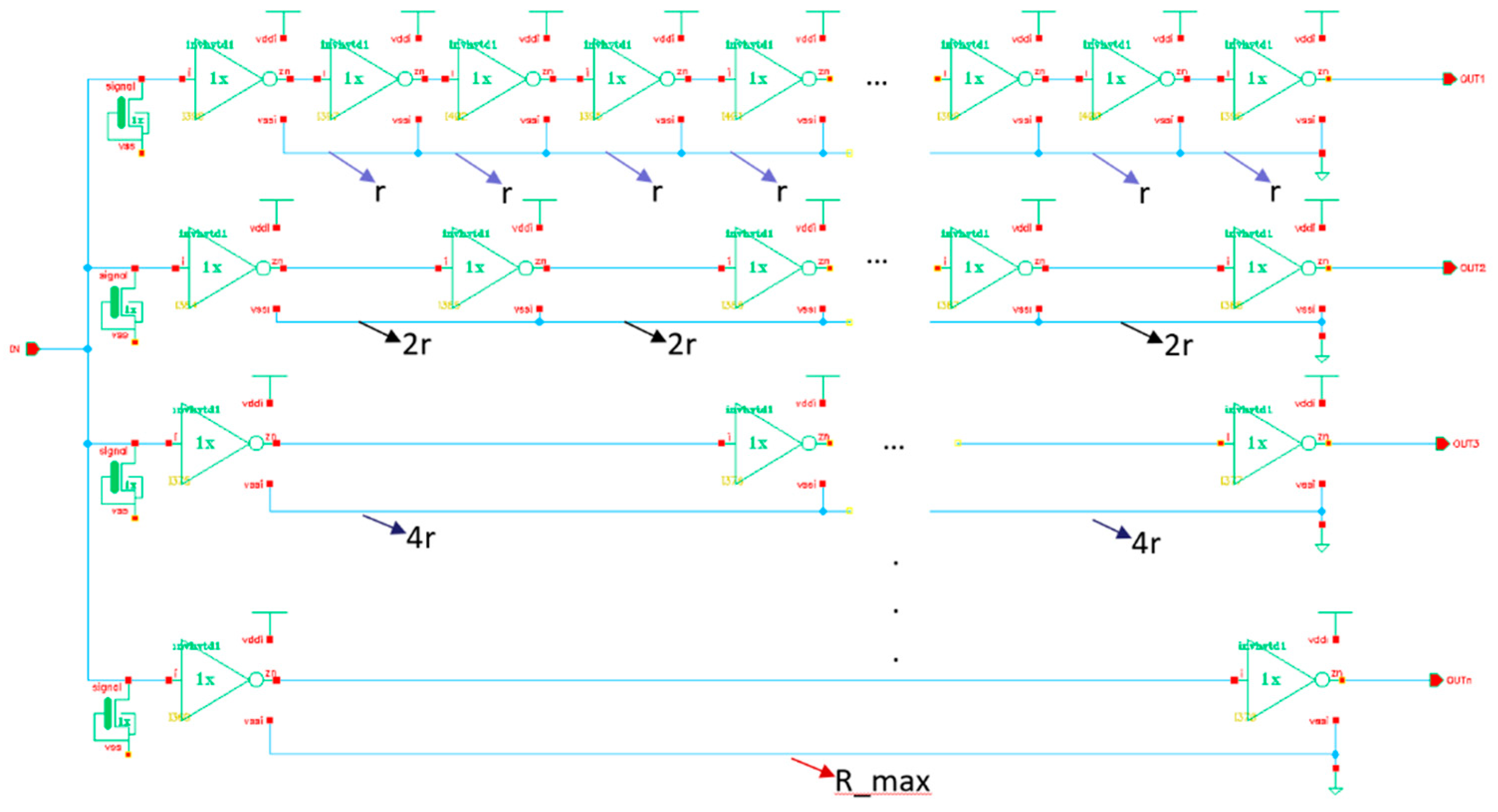
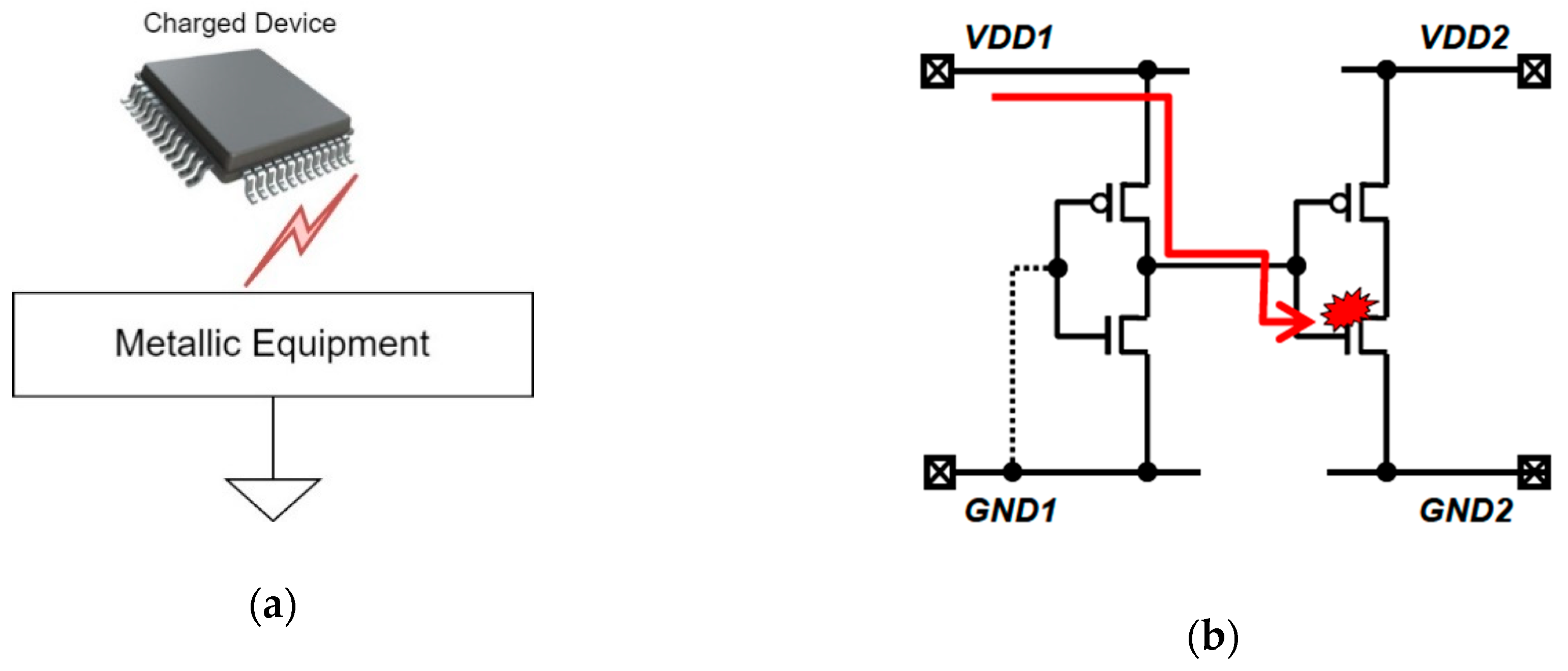
  • CDM is our major ESD concern and the focus of the proposed structure. The design of the proposed test-chip will permit to have a quantifiable ground resistor value in relationship with different CDM stress voltages according to JEDEC (Joint Electron Device Engineering Council) [11].
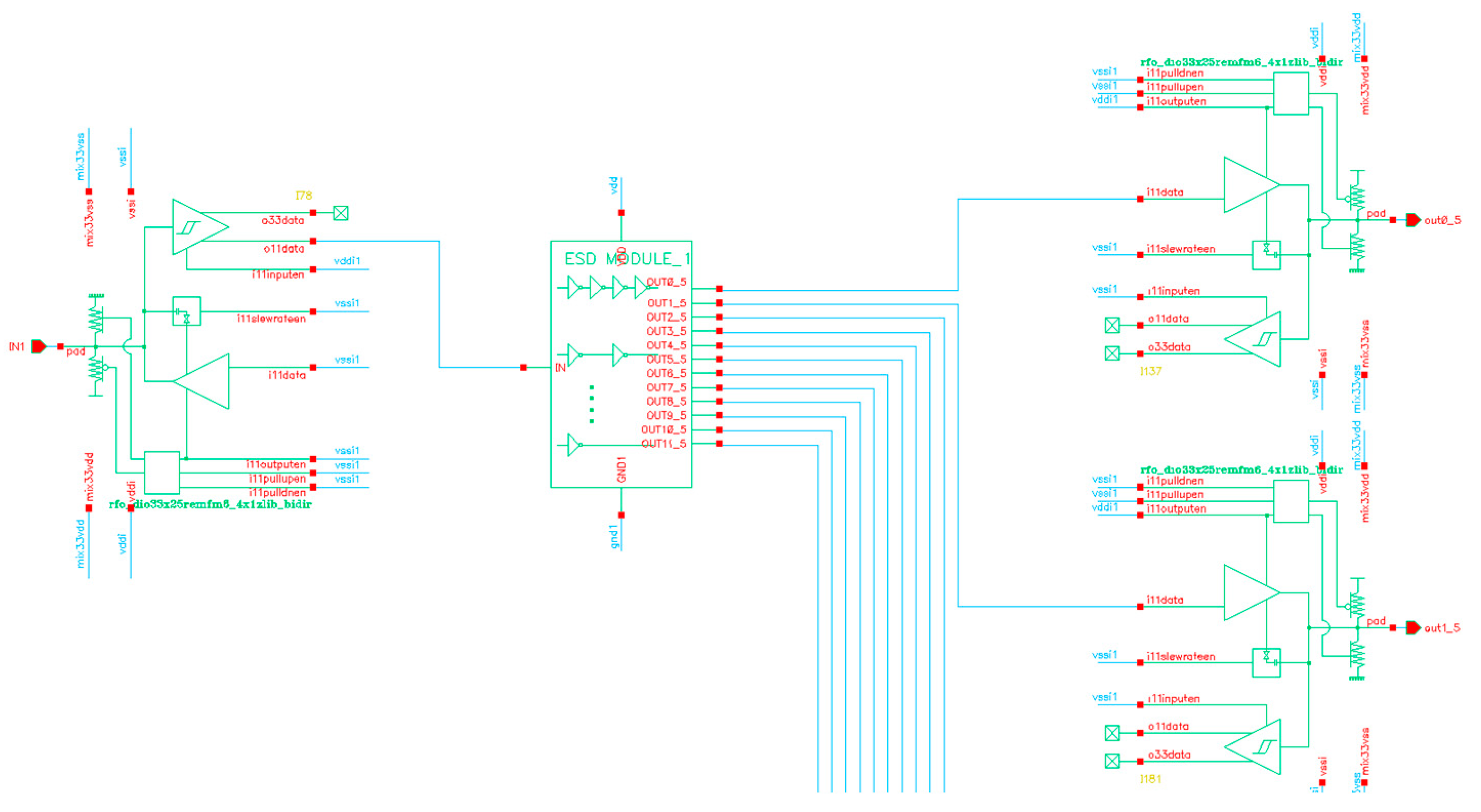
  • The I/O structures that will be used to connect the defined structure from the core to the package’s pins were previously designed and CDM tested and validated with a high CDM stress level. Hence the I/O structures do not constitute a threat for the present discussion.
  • Only one voltage domain was used to disregard the extra protections needed in that case [7,10] and to keep the sole focus on the ground-resistance effect.
  • Extra CDM protections such as GGNMOS (grounded gate NMOS) devices will be used to protect the gate oxide of the driver. The receiver in the structures that will be shortly defined are the object of our investigation.
CDM effect combined with purposely long ground wires that lead to high ground resistance can cause failures in the receiver. The focus of the analysis will be to determine the value of ground bus resistance for which the device will fail in relation to various CDM stress levels. It is important to quantify maximum allowed resistance while CDM protected for the 40 nm technology node.
In order to assess the ground resistance impact accurately in case of an ESD CDM event, the structure in Figure 4 was considered. The number of connected inverters for each row was calculated such as the wire resistance between two inverters’ supply will double with each row. The input pin is common for all rows whereas the outputs are separate. This way, the functionality can be properly tested per each row. Depending on the outcome for each row, the maximum wire resistance allowed can be established with high accuracy. The principle of doubling the resistance of the power rail with each row was kept. There are a total of 12 rows. The presumption was, as defined in the theoretical structure in Figure 4, that the latest row only contains 2 inverters with the highest wire resistance between the 2 inverters and going on the upper rows that resistance will decrease by a factor of 2. The main purpose is to apply CDM stress at the input and observe each output—if it failed or not—that way we will be able to conclude a maximum resistance for ground power rails. To keep the focus of the proposed structure only on the ground resistance effect over CDM event, GGNMOS devices have been placed at the beginning of each row. This ensures the protection of the first inverter’s gate oxide in case of a CDM event. There is only one supply voltage level across the structure, hence no other CDM protection method was needed between the other inverters of each row. If charge accumulates inside the chip and discharges through a high-resistive ground path, we will be able to conclude if the resistance of the ground bus was fairly low as to not cause a catastrophic CDM event.
Table 1 contains information about the number of inverters in each row and the resistance of the power track between two consecutive inverters. The first row of the module, where the inverters are very close to one another, contains a total number of 2346 inverters. The supply track length between two inverters is the lowest, leading to a ground track resistance of 0.57 ohms. Similarly, the last row only has 2 inverters with the longest wire length and a calculated resistance for ground track of around 1.4 k ohms. This information will be useful after the CDM stress of the testchip because the results of the test will be correlated with the track resistance for each row.
Figure 5a is a snapshot of the implemented schematic of the described structure. The whole schematic could not be captured and only a part of it is shown here. Figure 5b is a zoomed area of the schematic, where the tap cell, together with filler cell and the inverters can be seen.
The extra cells (GGNMOS, tap cell and filler cell) have the following purpose:
(a)
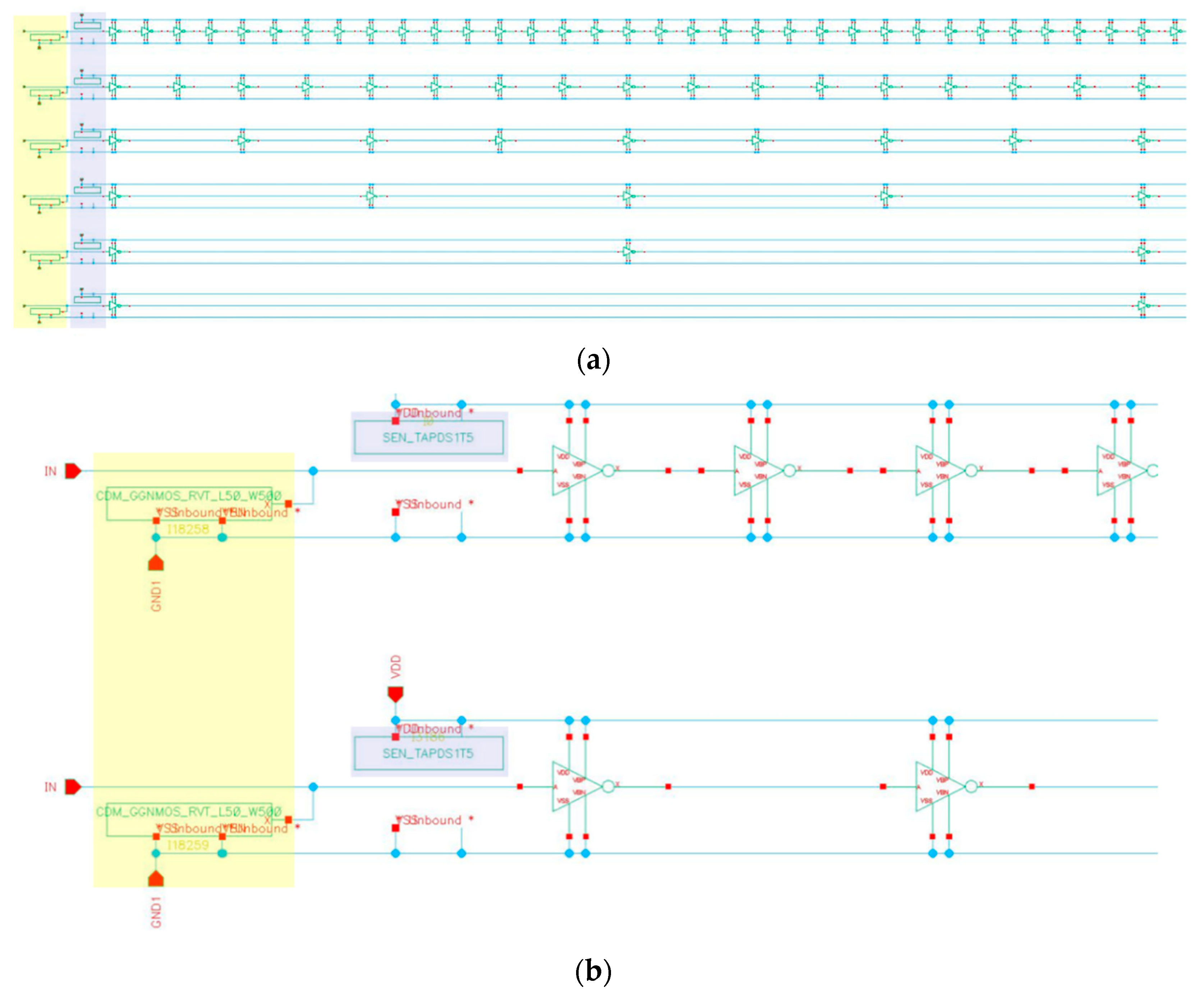
Input GGNMOS protection structure was added at the beginning of each row to protect the gates of the first inverter in case of ESD stress. Because the aim of the proposed structure is to see which is the maximum wire resistance where CDM stress does no harm, it was mandatory for the added input GGNMOS so that the eventual CDM faults in the output would be due to the length of the wires and not because of unprotected input signals. The input protection GGNMOS was highlighted in Figure 5b with semi-transparent yellow boxes.
(b)
Tap cells were added in order to correctly connect the bulk from the inverters from GGNMOS to corresponding potentials. Tap cells provide the nwell and substrate contacts, connecting pmos bulk (VBP) and nmos bulk (VBN) to the specified supply potentials. The purpose of this tap cell is for normal usage without bias or retention. Key characteristics are: VBP internally connected to the supply (VDD) and VBN internally connected to the ground (VSS). Tap cells were also highlighted in Figure 5b.
(c)
Filler cells were added in the layout to overcome design rule checking (DRC) errors. If a block has a halo/placement keepout region around it when it is placed on a chip, then the NOPG (fille cell without power/ground rails) end caps can be placed in the halo. Halos around blocks are used to provide room for routing power/ground supply rings, and for routing signal nets connecting to the block’s input/output pins. The use of NOPG cells in the halo does not consume any routing tracks the way fillers with VDD/VSS rails.
In Figure 6a is the entire layout implementation of the defined structure, with a total dimension of 1004.46 µm width and 39.1 µm height. The details cannot be well seen because of the large dimensions, that is why Figure 6b,c are zoomed in versions of the layout. Figure 6b contains the first part of the first seven rows of the entire layout. Figure 6c shows another zoomed in perspective with only 2 inverters gates having a 4.5 ohms supply wire resistance between them.
This layout implementation was sent to the designated foundry for silicon implementation of the structure. The test-chip implementation details will be described in the second part of this chapter.

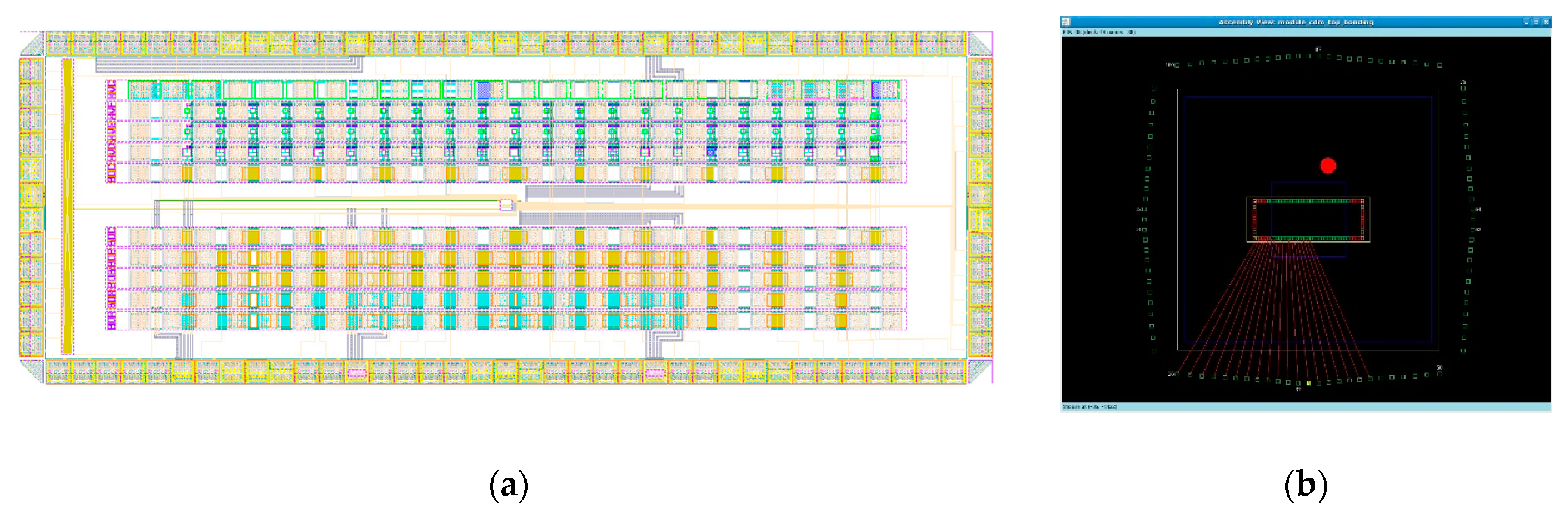
2.2. Test-Chip Implementation

The “CDM ground resistance” module was implemented in a test-chip. Apart from the complete package (symbol, schematic, layout), an I/O library was used for bonding and it created a pad ring that corresponds to each input, output, supply and ground pins. Figure 7 gives the schematic view of the module’s connection using bidirectional I/O cells. The input of the module is connected via an I/O cell defined as an input cell and the output of the I/Os are connected through bidirectional cells defined as output cells. The core voltage is in the 1.1 V domain, so signal o11data is used for the input defined cell and signal i11data is used for the output defined cell.
A total of 13 I/O bidirectional cells were used: one I/O cell defined as input cell for the module’s input and the rest of 12 I/O cells defined as output IOs for the output signals.
The entire layout of the testchip can be seen in Figure 8a. Surrounded by the I/O ring formed by a total of 102 IO cells (2 input/67 output/29 supply and ground cells/4 corner cells). The defined CDM module is in the left part with a total area of 39,274.38 µm2. Testchip also includes other structures for technology development so we can avoid empty area and be close to a real-chip development. The dimensions of the testchip are 3303 µm length and 1198 µm height.
The designated test-chip was a host for other modules as well, with a total of 96 pins necessary for the package. Due to the high number of IOs, the package chosen for this testchip is LQFP100. Part of the bonding diagram is given in Figure 8b.

3. Testing the Implemented Structures

The aim for this module is to link a certain ground resistance (corresponding to a calculated metal length) with the maximum ESD–CDM stress that it can withstand for the considered technology.

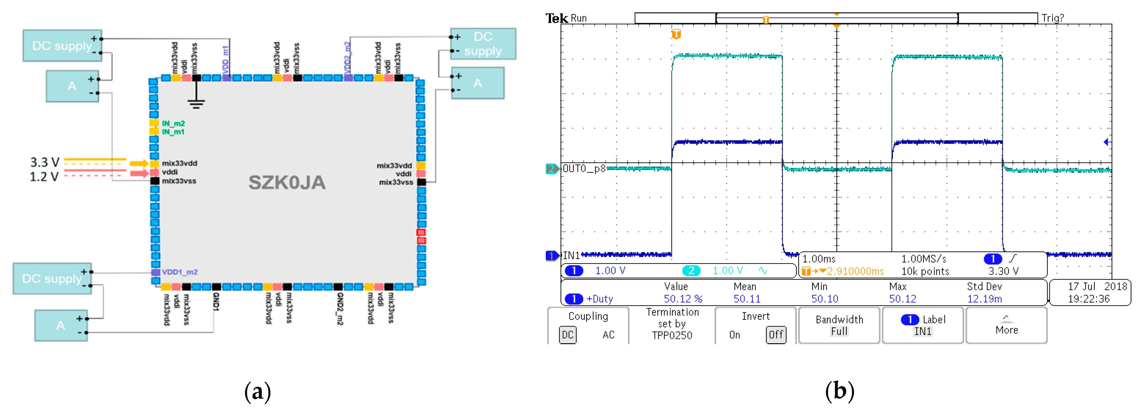
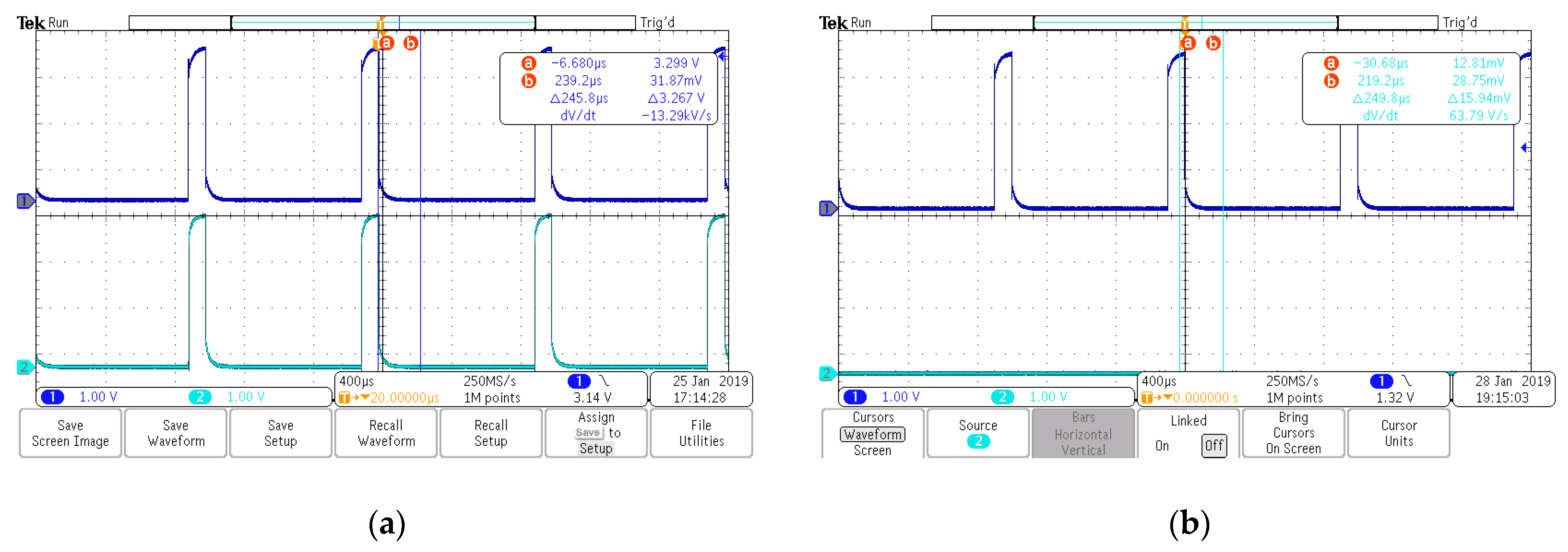
3.1. Functionality Testing

A total of 13 samples had to be tested. The setup for the test that will be done on each sample is illustrated in Figure 9a. The main test involved was a functional test. Given the fact that the module is mainly constructed out of inverters, we were only interested in the logical states of the output signal in relationship with the input signal. This test was undertaken with alternating current (AC) signals for some of the samples, to check that the inversion is correctly done (Figure 9b) and with direct current (DC) signals for all samples because it was faster to observe.
The functional tests performed on the implemented test chip were done to assess if the initial design, layout implementation and all the fab processes and the encapsulation process were undertaken correctly. Figure 9b contains an oscilloscope image of the input signal named “IN” and the output signal named “OUT0_p8” which corresponds to row 8 of the designed structure. According to Table 1, row 8 of the module contains 20 inverters and the expected result is that the output and input signals have the same polarity. Figure 9b confirms that the functionality for the specified row is the expected one. Similarly, all the outputs were tested for all the 13 samples and the results were stored as a reference to be used post-CDM stress.

3.2. Electrostatic Discharge–Charge Device Model (ESD–CDM) Stress

The next step in the study was to CDM-ESD stress the samples that were already functional tested. To do that, an ESD Orion2 CDM Machine was used. The default test method is field charge, or it can be also direct charge. The standards followed are: ESDA [1,2], JEDEC [11] and AEC [12].
The request for ESD-CDM stress was done with several key points:
  • Only the module’s ground and supplies to be stressed.
  • Only positive zaps per each supply/ground pin.
  • To be used three consecutive zaps per each pin.
  • To be used three samples per identical stress level.
For the first iteration, there were chosen only 12 samples to be stressed at: 500 V, 1 kV, 1.5 kV and 2 kV. The CDM stress voltage levels were considered carefully following the latest research on the market in terms of technology nodes used [13], packaging and industry applications [11,14].
The pins that will be CDM stressed using Orion2 machine were chosen such as to observe a direct CDM type of discharge on the test module: only supply and ground pins of the core are to be stressed because the I/Os that manage to send the signal from the outside world to the core chip and vice versa do not have CDM protections integrated. Pins stressed with positive and negative zaps were pin 31 that corresponds to the ground pin and pin 94 of the package that corresponds to the supply pin.

3.3. Functionality Testing Post ESD–CDM Stress

After the samples were stressed, the functional tests were re-done using the same test equipment, the same printed circuit board (PCB), and the same socket. The environmental parameters (temperature, noise level, test engineers) were kept identical for a clear comparison.
Figure 10 shows an oscilloscope picture after functionality testing post-CDM stress. Figure 10a contains the functionality test for the first row of the module after a 500 V CDM stress; this corresponds to the lowest ground wire resistance of 0.41 ohms. It is expected that the output signal has the same polarity as the input and the test confirmed this behavior even after CDM stress was performed. The conclusion is that for a very low ground wire resistance, under 1 ohm, after a CDM stress of 500 V, the core side of the chip is not affected, so lengths equivalent to resistance under 1 Ohm can be safely used in designing of integrated circuits in submicronic technologies.
Figure 10b shows an oscilloscope picture with the output corresponding to the last row, that has a ground metal resistance of 1.38 kohm. The expected output would have been for the signal to be inverted, but, under a transient pulse at the input, the output remains stuck at “0” logic level. It can be concluded from here that under an ESD–CDM stress of 2 kV for a design that includes a long wire with high resistivity for ground path, the chip will be damaged due to CDM phenomena.
For all other outputs of the designed structure (corresponding to different wire resistances defined in Table 1) and all CDM-stressed samples, DC tests were performed to verify the functionality. Table 2 contains all functionality results obtained post-CDM stress. The first column represents the wire resistance calculated for each row. A total of 13 samples were used for the experiment, one remaining un-stressed for functionality reference.
Three different samples were stressed at the same voltage level to verify if the results are reliable. The green boxes marked as “pass” indicate that the corresponding wire resistance has a good post-CDM stress functionality at the given CDM stress level shown in the first row of the table. The red boxes marked as “fail” indicate that the calculated wire resistance of the module gives faulty functionality post-CDM stress at the specific CDM voltage.
Following the information in Table 2, it can be concluded that:
  • All samples have good functionality after being stressed at 500 V and 1 kV. Therefore, for 500 V CDM stress all implemented ground wire resistors are safe to be used for the considered submicron technology. According to the latest research [13,14], CDM stress voltage at 500 V is enough to assure CDM protection for integrated circuits.
  • For 1.5 kV stress voltage, there are two situations: one sample failed for the row corresponding to 1.14 Ohm per ground length and two samples failed for the row with the maximum resistance of 1.38 kohm. We can conclude that for ground track resistance of 1.38 kohm, the part will fail when stressed at 1 kV CDM stress since 2 out of 3 samples failed. Regarding the second row corresponding to 1.14 ohm that had one sample failed, it can be considered a singular situation given the fact that the other two samples had good behavior at the same CDM voltage stress and all other rows with resistance higher than that passed the test.
  • For 2 kV stress voltage, there is only one sample that failed for the row corresponding to 1.14 ohm and it can be considered a non-repetitive pattern with no conclusion to be drawn, especially because on the next other cases with higher track resistivity there is no fail on neither of the samples. On the other hand, for the last row of the module corresponding to the maximum resistance of 1.38 kohm all three samples failed after performing the functionality test. The conclusion here is clear: the resistance of the supply tracks cannot exceed 1.38 kohm if CDM stress is above 1 kV.

4. Discussion

Among CDM protection rules, there is a very important aspect regarding the maximum permitted ground track resistance versus different values of CDM ESD stress [10]. This aspect is of high importance during I/O design process dues to the great distance between I/O structures and standard cell designs observed in chips. This research proposed to find the maximum allowed track resistance that can be CDM safe and can be used during I/O design process in the considered submicronic technology. To achieve this goal, a test structure was defined, implemented, and CDM stressed at different voltages. Finally, a direct link between track resistance values and the maximum allowed CDM stress was achieved.
After the test-chip implementation, 13 samples were tested for good functionality having as a reference the simulations performed in pre-silicon software tools. The next step was to CDM stress the samples at 4 different levels: 500 V, 1 kV, 1.5 kV and 2 kV with an Orion2 machine. After the first 12 samples were stressed, they were sent back for functional test in the same laboratory to use the identical equipment. Functional tests were performed again (post-CDM stress functionality verification) having as a reference the functionality results obtained pre-CDM stress. All these steps and the results obtained are described in this paper. After the previously defined methodological steps were followed, the conclusion that can be drawn is that there is a clear limitation for wire resistance that exceeds 1.3 kohm for cases where the CDM stress is 1 kV or higher.
Table 3 summarizes a comparative analysis with similar studies [20,21,22,28]. The analysis takes into account the technology node of each study, the package used for encapsulation, if the analyzed structures had different power domain, CDM stress level and the resulted maximum ground wire resistance for which the chip is still CDM protected. A similar investigation [20] considers different power domains with GGNMOS receiver gate protection. The resistance between the GGNMOS source and the receiver paper [21] proposes the same inter-power domain analysis in six different configurations inverter is the equivalent of this study’s ground resistance. Another one of the configurations aims at a simple structure with only a large ground bus resistance to be taken into account while the CDM stress is being performed. A case with very thin Tox in a 130 nm technology is being presented [22] along with its results in terms of CDM protection while considering ground net resistance impact. The last item chosen for comparison [28] is an investigation in a 90 nm technological node that considers a single-domain case to investigate the contribution of ground net resistance to CDM failures. It is to be noted that this comparison is important in terms of quantifying the maximum ground wire resistance for a large spectrum of technological nodes. In this paper a nanometre channel length is considered.
The defined module needs to be stressed at a higher CDM voltage so that a fair conclusion can be drawn for supply track resistances lower than the maximum defined limit of 1.38 kohm. One limitation comes from Orion2 machine used for CDM stress that cannot exceed a 2 kV stress voltage. To reach the desired effect, another standard will be used. All the procedures described in CDM stress in this paper were undertaken with the JS-002 standard: each stressed voltage corresponds to different maximum currents injected, depending on the package size. For the other standard, named ANSI/ESDA (electrostatic discharge avoidance) [1,2], the currents for the same stress voltage are slightly higher. The aim is to re-iterate the stress voltage and to try with the other standard and to see if there is a notable difference in functionality.

5. Conclusions

Prediction was the key word in our research. The aim of the proposed structure was to predict an accurate ground resistance value for which a CDM event might cause catastrophic failures in the core of a chip designed in a 40 nm technology node. By taking all necessary precautions, potential weaknesses (such as discontinuities in the power network, extra CDM protection added) might have been neglected.
The implemented module considered various cases with different ground lengths that corresponds to different resistances. The module was tested for good functionality, sent to CDM stress at four different voltages (500 V, 1 kV, 1.5 kV and 2 kV) and tested again for post-CDM stress.
After the aforementioned testing process, the conclusion is that ground resistance values lower than 690 ohm are safe to be used in the routing process, as the functional tests passed after all CDM stress voltages considered. The last designed row corresponding to the highest ground bus resistance (1.38 kohm) failed at functional testing post-CDM stress for two cases: (1) all three samples failed functional testing after 2 kV CDM stress and (2) two out of three samples failed functional testing after 1.5 kV CDM stress. The same row passed the functional testing post CDM stress when the stress voltage was 1 kV and 500 V. The conclusion in this case is that a 1.38 kohm ground resistance can be used when routing a chip in the considered 40 nm technology node, as long as the required CDM stress voltage level is less or equal to 1000 V.
A comparative analysis with other similar studies showed the same direction in terms of conclusions: shorter metal connections with lower power/ground resistivity are to be preferred to avoid unwanted behavior in case of a CDM event. The novelty of this paper is that it quantifies the resistance value for which CDM event does not trigger a catastrophic failure on the chip’s functionality. This have been done considering the technology node limitations and with high attention to the specific design rules and limitations given by the foundry.
The findings from this investigation have already been used as know-how in all I/O development projects in the targeted technology.

Author Contributions

Conceptualization, M.-D.D., P.C. and G.B.; methodology, M.-D.D. and P.C.; validation, M.-D.D.; investigation, M.-D.D.; writing—original draft preparation, M.-D.D.; writing—review and editing, M.-D.D., P.C. and G.B.; visualization, G.B.; supervision, P.C. All authors have read and agreed to the published version of the manuscript.

Funding

Part of the publication has been founded by the Operational Programme of the Ministry of Europe Funds through the Financial Agreement 51675/09.07.2019 POCU380/6/13, SMIS code 125125.

Conflicts of Interest

The authors declare no conflict of interest.

References

  1. ESD Association. Fundamentals of Electrostatic Discharge, Part Five—Device Sensitivity and Testing; ESD Association: Rome, NY, USA, 2010; p. 2. [Google Scholar]
  2. ESD Association. Fundamentals of Electrostatic Discharge, Part 1—An Introduction to ESD; ESD Association: Rome, NY, USA, 2010. [Google Scholar]
  3. Duvvury, C.; Amerasekera, A. Advanced CMOS protection device trigger mechanisms during CDM. IEEE Trans. Compon. Packag. Manuf. Technol. Part C 1996, 19, 169–177. [Google Scholar] [CrossRef]
  4. Neil, D.M.H.; Weste, H.E. CMOS VLSI Design, a Circuits and Systems Perspective, 4th ed.; Pearson Education Inc.: London, UK, 2011; pp. 593–594. [Google Scholar]
  5. Ker, M.D.; Hsiao, Y.W. CDM ESD protection in CMOS integrated circuits. In Proceedings of the 2008 Argentine School of Micro-Nanoelectronics, Technology and Applications, Buenos Aires, Argentina, 18–19 September 2008; pp. 61–66. [Google Scholar]
  6. Aharoni, E.; Parvin, A.; Vaserman, Y.; Grund, E. Empirical ESD simulation flow for ESD protection circuits based on snapback devices. In Proceedings of the 2016 38th Electrical Overstress/Electrostatic Discharge Symposium (EOS/ESD), Garden Grove, CA, USA, 11–16 September 2016; pp. 1–10. [Google Scholar] [CrossRef]
  7. Okushima, M. ESD protection design for mixed-power domains in 90 nm CMOS with new efficient power clamp and GND current trigger (GCT) technique. In Proceedings of the 2006 Electrical Overstress/Electrostatic Discharge Symposium, Anaheim, CA, USA, 10–15 September 2006; pp. 205–213. [Google Scholar]
  8. Chen, S.; Ker, M.; Hung, H. Active ESD Protection Design for Interface Circuits between Separated Power Domains against Cross-Power-Domain ESD Stresses. IEEE Trans. Device Mater. Reliab. 2008, 8, 549–560. [Google Scholar] [CrossRef]
  9. Watanabe, K.; Hiraoka, T.; Sato, K.; Sei, T.; Numata, K. New protection techniques and test chip design for achieving high CDM robustness. In Proceedings of the EOS/ESD 2008—2008 30th Electrical Overstress/Electrostatic Discharge Symposium, Tucson, AZ, USA, 7–11 September 2008; pp. 332–338. [Google Scholar]
  10. Etherton, M.; Ruth, S.; Miller, J.W.; Agarwal, R.; Bhooshan, R.; Ershov, M.; Cadjan, M.; Feinberg, Y.; Srinivasan, K.; Chang, N.; et al. A new full-chip verification methodology to prevent CDM oxide failures. In Proceedings of the 2015 37th Electrical Overstress/Electrostatic Discharge Symposium (EOS/ESD), Reno, NV, USA, 27 September–2 October 2015; pp. 1–10. [Google Scholar] [CrossRef]
  11. Recommended ESD-CDM Target Levels; JEDEC Publication JEP157; JEDEC Solid State Technology Association: Arlington County, VA, USA, 2009; p. 11.
  12. Charged Device Model (CDM) Electrostatic Discharge Test. AEC—Q100-011 Rev-C1. 12 March 2013. Available online: http://www.aecouncil.com/Documents/AEC_Q100-011C1.pdf (accessed on 12 May 2017).
  13. Kim, S.; Sithanandam, R.; Seo, W.; Lee, M.; Cho, S.; Park, J.; Kwon, H.; Kim, N.; Jeon, C. Technology Scaling of ESD Devices in State-of-the-ArtFinFET Technologies. In Proceedings of the 2020 IEEE Custom Integrated Circuits Conference (CICC), Boston, MA, USA, 22–25 March 2020; pp. 1–6. [Google Scholar] [CrossRef]
  14. White Paper 1: A Case for Lowering Component Level HBM/MM ESD Specifications and Requirements; Industry Council on ESD Target Levels, June 2018; Available online: https://www.esdindustrycouncil.org/ic/docs/industry%20council_esd_target_levels_whitepaper1_rev4.0_june2018%20final.pdf (accessed on 28 December 2020).
  15. Shukla, V.; Jack, N.; Rosenbaum, E. Predictive simulation of CDM events to study effects of package, substrate resistivity and placement of ESD protection circuits on reliability of integrated circuits. In Proceedings of the 2010 IEEE International Reliability Physics Symposium, Anaheim, CA, USA, 2–6 May 2010; pp. 485–493. [Google Scholar] [CrossRef]
  16. Ershov, M.; Feinberg, Y.; Cadjan, M.; Klein, D.; Etherton, M. EDA software for verification of metal interconnects in ESD protection networks at chip, block, and cell level. In Proceedings of the 2013 35th Electrical Overstress/Electrostatic Discharge Symposium, Las Vegas, NV, USA, 10–12 September 2013; pp. 1–7. [Google Scholar]
  17. Abessolo-Bidzo, D.; Smedes, T.; Huitsing, A.J. CDM Simulation Based on Tester, Package and Full Integrated Circuit Modeling: Case Study. IEEE Trans. Electron Devices 2012, 59, 2869–2875. [Google Scholar] [CrossRef]
  18. Shukla, V.; Boselli, G.; Dissegna, M.; Duvvury, C.; Sankaralingam, R.; Rosenbaum, E. Prediction of Charged Device Model Peak Discharge Current for Microelectronic Components. IEEE Trans. Device Mater. Reliab. 2014, 14, 801–809. [Google Scholar] [CrossRef]
  19. Olson, N.; Shukla, V.; Rosenbaum, E. Test Chip design for study of CDM related failures in SoC designs. In Proceedings of the 2011 International Reliability Physics Symposium, Monterey, CA, USA, 10–14 April 2011; pp. EL.3.1–EL.3.6. [Google Scholar] [CrossRef]
  20. Abessolo-Bidzo, D.; Smedes, T.; de Jong, P.C. A study of the effect of remote CDM clamps in integrated circuits. In Proceedings of the 2015 37th Electrical Overstress/Electrostatic Discharge Symposium (EOS/ESD), Reno, NV, USA, 27 September–2 October 2015; pp. 1–8. [Google Scholar] [CrossRef]
  21. Troussier, C.; Bourgeat, J.; Simeu, E.; Arnould, J.-D.; Jimenez, J.; Jacquier, B. Study of Inter-Power Domain Failures during a CDM Event. In Proceedings of the 2020 42nd Annual EOS/ESD Symposium (EOS/ESD), Reno, NV, USA, 13–18 September 2020; pp. 1–5. [Google Scholar]
  22. Brennan, C.J.; Sloan, J.; Picozzi, D. CDM failure modes in a 130 nm ASIC technology. In Proceedings of the 2004 Electrical Overstress/Electrostatic Discharge Symposium, Grapevine, TX, USA, 19–23 September 2004; pp. 1–5. [Google Scholar] [CrossRef]
  23. Di Biccari, L.; Boroni, A.; Castelnovo, A.; Zullino, L.; Cerati, L.; Wolf, H.; Weber, J.; Andreini, A. Impact of Alternative CDM Methods on HV ESD Protections Behavior. In Proceedings of the 2020 42nd Annual EOS/ESD Symposium (EOS/ESD), Reno, NV, USA, 13–18 September 2020; pp. 1–10. [Google Scholar]
  24. Dumalkina, E.; Semenov, O. Optimization of Metal Interconnects in I/O Cells and Banks to Improve Robustness of ESD Protection Network in 16 nm FinFet Technology. In Proceedings of the 2020 International Semiconductor Conference (CAS), Sinaia, Romania, 7–9 October 2020; pp. 69–72. [Google Scholar] [CrossRef]
  25. Zhou, Y.; Hajjar, J. CDM ESD failure modes and VFTLP testing for protection evaluation. In Proceedings of the 2008 9th International Conference on Solid-State and Integrated-Circuit Technology, Beijing, China, 20–23 October 2008; pp. 333–336. [Google Scholar] [CrossRef]
  26. Brennan, C.J.; Kozhaya, J.N.; Proctor, R.A.; Sloan, J.; Chang, S.; Sundquist, J.; Lowe, T. ESD design automation for a 90nm ASIC design system. In Proceedings of the 2004 Electrical Overstress/Electrostatic Discharge Symposium, Grapevine, TX, USA, 19–23 September 2004; pp. 1–8. [Google Scholar] [CrossRef]
  27. Brodbeck, T.; Esmark, K.; Stadler, W. CDM tests on interface test chips for the verification of ESD protection concepts. In Proceedings of the 2007 29th Electrical Overstress/Electrostatic Discharge Symposium (EOS/ESD), Anaheim, CA, USA, 16–21 September 2007; pp. 1A.1-1–1A.1-8. [Google Scholar] [CrossRef]
  28. Alvarez, D.; Kupfer, C.; Kruppa, J.; Trivedi, N.J.; Chakravarthy, S.N. CDM single power domain failures in 90 nm. In Proceedings of the 2013 35th Electrical Overstress/Electrostatic Discharge Symposium, Las Vegas, NV, USA, 10–12 September 2013; pp. 1–8. [Google Scholar]
Figure 1. Charge device model (CDM) occurrence: (a) the pin touches a grounded metallic surface; (b) CDM electrostatic discharge (ESD) current path in an input buffer.
Electronics 10 00443 g001
Figure 2. Long wire effect with CDM stress [10] (Copyright 2021 with permission from author; license number 5004691247069); if there is a source of CDM stress and it comes across a long wire (that forms a large wire resistance), the damage can be catastrophic.
Electronics 10 00443 g002
Figure 3. Methodology for maximum ground wire resistance definition while CDM protected.
Electronics 10 00443 g003
Figure 4. CDM module structure and principle: each row will double the length of the ground wire. The module’s lowest ground resistance value was noted “r” and the module’s highest ground resistance value is noted R_max~211 × r.
Electronics 10 00443 g004
Figure 5. (a) Part of the schematic; (b) zoomed in schematic view.
Electronics 10 00443 g005
Figure 6. (a) Entire layout of the defined module (1004.46 µm × 39.1 µm dimensions); (b) zoomed in view for the first seven rows; (c) zoomed in view of two inverters connection.
Electronics 10 00443 g006
Figure 7. Example of inputs and outputs (I/Os) as connections for bidirectional cells.
Electronics 10 00443 g007
Figure 8. (a) Layout implementation of the entire test chip; (b) bonding diagram example.
Electronics 10 00443 g008
Figure 9. (a) Test setup used for functionality verification; (b) oscilloscope image of the transient result for input and output pins corresponding to the eighth row of the module.
Electronics 10 00443 g009
Figure 10. Functionality tests performed on one sample after CDM stress: (a) transient signals shown on oscilloscope for first row stressed at 500 V; (b) transient signals shown on oscilloscope for last row stressed at 2 kV.
Electronics 10 00443 g010
Table 1. Relationship between number of inverters and supply track resistance for each row of the designed structure.
Row NumberNo. of InvertersResistance [ohm]
123460.57
211721.14
35872.28
43064.56
51539.12
67718.24
73936.58
82072.65
910155.44
105344.78
113690.55
1221387.17
Table 2. Results of post-CDM stress functionality.
Wire Resistance [ohm]CDM Stress Applied
0 V500 V500 V500 V1000 V1000 V1000 V1500 V1500 V1500 V2000 V2000 V2000 V
0.57passpasspasspasspasspasspasspasspasspasspassfailpass
1.14passpasspasspasspasspasspassfailpasspasspasspasspass
2.28passpasspasspasspasspasspasspasspasspasspasspasspass
4.56passpasspasspasspasspasspasspasspasspasspasspasspass
9.12passpasspasspasspasspasspasspasspasspasspasspasspass
18.24passpasspasspasspasspasspasspasspasspasspasspasspass
36.58passpasspasspasspasspasspasspasspasspasspasspasspass
72.65passpasspasspasspasspasspasspasspasspasspasspasspass
155.44passpasspasspasspasspasspasspasspasspasspasspasspass
344.78passpasspasspasspasspasspasspasspasspasspasspasspass
690.55passpasspasspasspasspasspasspasspasspasspasspasspass
1387.17passpasspasspasspasspasspassfailpassfailfailfailfail
Table 3. Performance analysis with similar studies.
Other Relevant PapersTechnology NodePackage UsedDifferent Power DomainsCDM Stress MethodCDM Stress VoltageMaximum Ground Wire Resistance
[20]250 nmLQFP64 (Low Profile Quad Flat Package)yesvf-TLP
(very fast TLP)
750 V1 kohm
[21]-CDIP (Ceramic Dual Inline Package)yesvf-TLP750 V5.8 kohm (GGNMOS added)
[22]130 mFlip-chipno-500 V1.5 ohm
[28]90 nmBGA (Ball Grid Array)no-600 V600 ohm
This paper40 nmLQFP100noFICDM (Field-Induced CDM)1 kV1.3 kohm
Publisher’s Note: MDPI stays neutral with regard to jurisdictional claims in published maps and institutional affiliations.

