Article

Analysis of a Wide Voltage Hybrid Soft Switching Converter

Department of Electrical Engineering, National Yunlin University of Science and Technology, Yunlin 640, Taiwan
*
Author to whom correspondence should be addressed.
Electronics 2021, 10(4), 473; https://doi.org/10.3390/electronics10040473
Submission received: 5 January 2021 / Revised: 9 February 2021 / Accepted: 9 February 2021 / Published: 16 February 2021
(This article belongs to the Special Issue Power Electronics in Industry Applications)

Abstract

:
A hybrid PWM converter is proposed and investigated to realize the benefits of wide zero-voltage switching (ZVS) operation, wide voltage input operation, and low circulating current for direct current (DC) wind power conversion and solar PV power conversion applications. Compared to the drawbacks of high freewheeling current and hard switching operation of active devices at the lagging-leg of conventional full bridge PWM converter, a three-leg PWM converter is studied to have wide input-voltage operation (120–600 V). For low input-voltage condition (120–270 V), two-leg full bridge converter with lower transformer turns ratio is activated to control load voltage. For high input-voltage case (270–600 V), PWM converter with higher transformer turns ratio is operated to regulate load voltage. The LLC resonant converter is connecting to the lagging-leg switches in order to achieve wide load range of soft switching turn-on operation. The high conduction losses at the freewheeling state on conventional full bridge converter are overcome by connecting the output voltage of resonant converter to the output rectified terminal of full bridge converter. Hence, a 5:1 (600–120 V) hybrid converter is realized to have less circulating current loss, wide input-voltage operation and wide soft switching characteristics. An 800 W prototype is set up and tested to validate the converter effectiveness.

1. Introduction

For past years, clean and sustainable energy has received increased attention to reduce greenhouse gas emissions and fossil energy demand. Photovoltaic (PV) solar cell, fuel cell stacks, and DC wind power are attractive sustainable energy sources as they are cost-effective [1,2,3,4]. The main drawback of these sustainable energy sources is that the output DC or AC voltage is not constant. To solve this problem, the soft switching high-frequency DC-DC converters have been developed by using switching frequency modulation [5,6], pulse-width modulation (PWM) [7,8,9,10], active clamp PWM [11,12], and asymmetric PWM [13,14] schemes. The main drawbacks of active clamp PWM and asymmetric PWM schemes are the unbalance current and voltage stresses on the rectifier diodes. In resonant converters, the operating switching frequency depends on the load power and input voltage so that the load voltage is controlled by frequency modulation. However, the wide output-voltage variation of sustainable energy sources will result in wide switching frequency deviation in resonant converters. In PWM scheme, the duty ratio (or duty cycle) on active devices or input leg voltage of PWM converter depends on input voltage. Thus, the duty cycle of PWM converter can be regulated to countract input voltage variation. Generally, the maximum (minimum) effective duty ratio deff,max (deff,min) is related to minimum (maximum) input voltage Vin,min (Vin,max). Due to duty loss problem at the freewheeling state on conventional phase-shift PWM converter, the effective duty ratio deff is usually designed to be greater than 0.15 and less than 0.45. Hence, input voltage variation will be limited at Vin,max/Vin,min = deff,max/deff,min < 3 on conventional phase-shift PWM operation. As the voltage deviation from PV panels and DC wind generator outputs may be greater than 3, the cascaded or parallel-connected circuit structures [15,16,17] have been developed to overcome this problem. However, the low efficiency is the main problem of cascaded PWM converters. In serial- and parallel-connected circuit topology with wide voltage operation in [15,16], the component counts, high circulating current, and the complicated control algorithm are the main disadvantages. However, the maximum voltage deviation in [15,16,17] is still less than 4 (Vin,max/Vin,min < 4). The DC converters with more than 5 (Vin,ma/Vin,min > 5) wide voltage capability are normally demanded for renewable energy.
A hybrid converter with a three-leg phase-shift PWM circuit and a LLC circuit are presented and realized to have benefits of wide load range of zero voltage switching (ZVS), less circulating current loss, and wide input voltage capability (120–600 V). On the basis of input voltage, two sub-circuits are selected to operate in order to overcome wide input-voltage deviation. One AC switch is adopted to select one of two sub-circuits under low or high input-voltage condition. Therefore, a 5:1 (Vin,max = 5 Vin,min) wide input voltage hybrid converter is achieved. The phase-shift PWM approach is used to control output voltage. Power devices at the leading leg can be easily turned on at ZVS because the output inductor energy is used to release energy stored on output capacitor of active devices. The hard switching disadvantage of lagging-leg active devices in conventional full bridge converter is overcome by connecting a LLC resonant circuit to the lagging-leg active devices. Therefore, the lagging-leg active devices are turned on at ZVS. In circuit implementation, a Schmitt comparator with a ±30 V hysteresis range is adopted to select the appropriate sub-circuit under high or low voltage input operation. The control scheme can be easily implemented by using logic gates, comparator, and phase-shift PWM integrated circuit. The benefits of the studied hybrid zero-voltage switching (ZVS) converter are confirmed by an 800 W experimental prototype.

2. Structure of the Proposed Converter

The converter diagram of conventional full bridge PWM converter is given in Figure 1a. The main benefit of full bridge PWM converter is ZVS operation on S1 and S2 (leading-leg switches). However, the full bridge PWM converter has several drawbacks. such as hard switching operation on S3 and S4 (lagging-leg switches) and high primary current loss at the freewheeling state vab = 0 when S1 and S3 are ON or S2 and S4 are ON. Therefore, serious switching losses can be generated at the lagging leg and high conduction losses will be generated on the primary side under low duty cycle condition. To overcome hard switching loss, a LLC resonant circuit (Lr T2, Cr, D3, D4, CLLC and D5) remark in red (Figure 1b) is adopted and connected to the lagging-leg switches. As LLC resonant circuit is operated at constant frequency (fsw = fr resonant frequency of Lr and Cr), active devices S3 and S4 can achieve ZVS operation. The other drawback of conventional PWM converter in Figure 1a is the serious circulating current loss at the freewheeling state vab = 0. To solve this problem, diode D5 is used to connect two voltage terminals Vo,LLC and VR on the secondary side. Therefore, the secondary rectified voltage VR is positive in Figure 1b instead of VR = 0 in Figure 1a during the freewheeling interval. During the forward power flow from Vin to Vo, the primary-side leg voltage |vab| ≈ Vin and the secondary rectified voltage VRVinns /np1 > Vo,LLC. Thus, diode D5 is reverse biased. Diode D5 is forward biased during the freewheeling interval (vab = 0). Because D5 is conducting, the energy on CLLC is transferred to Vo at the freewheeling state. In the freewheeling interval, the rectified voltage VR = Vo,LLC > 0, the primary inductor voltage VLR = −(np1/ns1)Vo,LLC, and the primary current iLR are decreased. For some renewable energy power conversions for solar power or wind power applications, the DC converters with wide voltage operation capability are needed in order to counteract wide input voltage variation. Conventional full bridge PWM converter can operate well with narrow voltage variation, such as Vin,max/Vin,min < 3. For more wide voltage deviation, the conventional full bridge PWM circuit cannot achieve this demand. To achieve wide voltage deviation request, three leg PWM converter is adopted and shown in Figure 1c. Comparing the circuit diagrams in Figure 1b,c, it can be noted, one more switch leg with components S1, S2, and Q remark in blue is adopted in the presented circuit. The transformer T1 has four winding turns np1, np1, ns1, and ns1. Switch Q is used to control turns ratio of T1 under the different input voltage regions.
When 120 V ≤ Vin < 270 V (low voltage region, Vin,L), the proposed converter with high voltage gain is requested to keep load voltage constant. Therefore, active devices Q, S1, and S2 are OFF, as shown in Figure 2a. Only S3S6 are activated to regulate Vo. Circuit S3S6, T1, LR, D1, D2, and Lo are activated as the full bridge phase-shift PWM converter. The leading-leg active devices S3 and S4 can easily turn on at ZVS operation. The turns-ratio of T1 is np1/ns1 under low voltage input range. Circuit structure with components S5, S6, T2, Lr, Cr, D3, D4, and CLLC is operated as the LLC series resonant converter. Due to the resonant behavior, the lagging leg active devices S5 and S6 are turned on at ZVS. When 270 V ≤ Vin < 600 V (high voltage region, Vin,H), Q is ON and S3 and S4 are OFF, as shown in Figure 2b. S1, S2, S5, and S6 are activated to control load voltage Vo. Circuit structure with components S1, S2, S5, S6, T1, LR, D1, D2, and Lo are activated as the full bridge phase-shift PWM circuit. The leading-leg active devices S1 and S2 turn on at ZVS. The turns-ratio of T1 in Figure 2b is 2np1/ns1 under high voltage input range. Due to LLC circuit connected to the lagging leg, S5 and S6 are turned on at ZVS. From the previous discussion, it is clear that the presented hybrid converter has soft switching operation, wide input-voltage operation (Vin,max/Vin,min = 5), and less primary current at the freewheeling state.

3. Principle of Operation

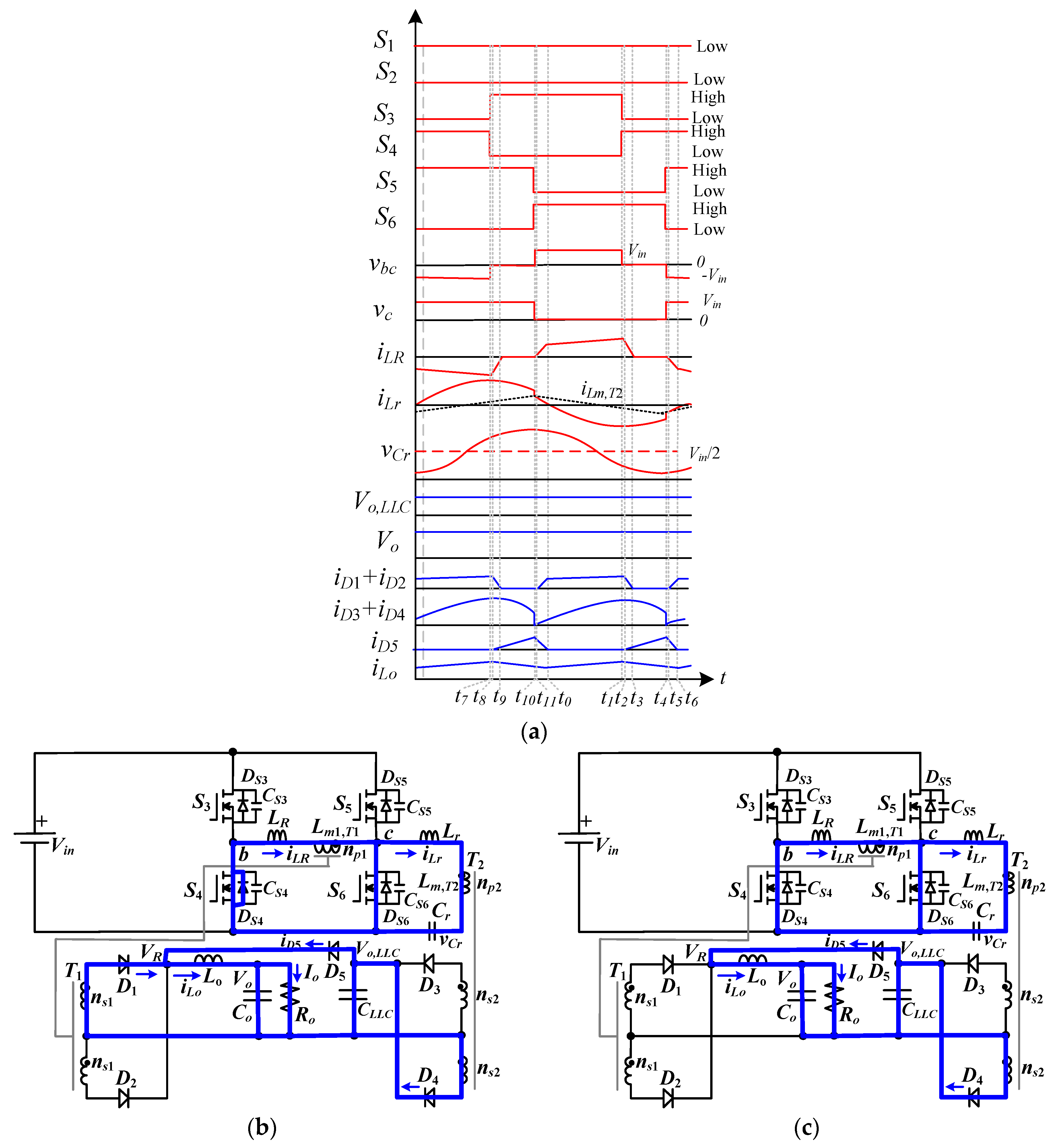
If Vin is in the low voltage region (Vin,L = 120–270 V), active devices Q, S1, and S2 are all turned off. Power switches S3S6 and passive components T1, LR, D1, D2, and Lo are operated with PWM approach to control load voltage Vo. LLC resonant circuit with components S5, S6, T2, Lr, Cr, D3, D4, and CLLC is operated with fixed switching frequency to achieve ZVS operation of S5 and S6. It is assumed the inductances Lm1 = Lm2 >> LR and capacitances CS1 = … = CS6 = Coss. The PWM waveforms under the low input-voltage region are given in Figure 3a. One can observe that there are six states (Figure 3b–g) in each half switching cycle. The PWM waveforms are symmetrical in every half switching period. To simplify the system analysis, only the operating states in the first half switching period are stated in this section.
State 1 [t0t < t1]: In state 1, S3 and S6 are in the on-state and leg voltage vbc = Vin. LLC converter is controlled at the resonant frequency. As S6 is in the on-state, iLr decreases and iLr < iLm,T2. The secondary diodes D1 and D4 are forward biased. The drain voltages vCS4 = vCS5 = Vin and the diode voltages vD2 ≈ 2 × Vin/(np /ns1) and vD3 ≈ 2 Vo,LLC. The currents iLo and iLR are expressed in Equations (1) and (2):
i L o ( t ) i L o ( t 0 ) + V i n n p 1 / n s 1 V o L o ( t t 0 )
i L R ( t ) i L R ( t 0 ) + V i n n p 1 V o n s 1 ( n p 1 / n s 1 ) 2 L o ( t t 0 )
State 2 [t1t < t2]: At t1, S3 turns off. As iLR(t1) > 0, CS4 is discharged by iLR after time t1. If the inductor energy [ L R + ( n p 1 / n s 1 ) 2 L o ] i L R 2 ( t 1 ) > 2 C o s s V i n 2 , vCS4 is decreased and will be equal to 0 at t2. The discharged time of CS4 is expressed as:
Δ t 12 ( 2 V i n C o s s n p 1 ) / ( I o n s 1 )
LLC converter is still controlled at the resonant mode to distribute power from Vin to Vo,LLC.
State 3 [t2t < t3]: At t2, vCS4 is decreased and equal to zero voltage. Since iLR(t2) > 0, DS4 is conducting and S4 can turn on to have soft switching operation. Due to vbc = 0, the diode D5 becomes forward biased and the rectified voltage VR is clamped at Vo,LLC. Therefore, the inductor voltages vLR = −np1Vo,LLC/ns1 < 0 and vLo = Vo,LLCVo < 0. iLR and iLo are decreased in this state.
i L o ( t ) i L o ( t 2 ) + V o , L L C V o L o ( t t 2 )
i L R ( t ) i L R ( t 2 ) n p 1 V o , L L C n s 1 L R ( t t 2 )
However, the conventional full bridge converter has vLR ≈ 0 and iLR ≈ constant in this state (freewheeling state). Therefore, the conventional full bridge PWM converter has more circulating current loss in this state. In Equation (5), one can observe the primary current iLR is decreased at freewheeling state in the proposed converter. If the time interval at freewheeling state is long enough, the diode current iD1 or the primary current iLR can be declined to zero.
Δ t i L R = 0 L R I o / [ ( n p 1 / n s 1 ) 2 V o , L L C )
The time ΔtiLp=0 is related to LR, Vo,LLC, and Io. Thus, more freewheeling time duration is required at full load to eliminate the circulating current.
State 4 [t3t < t4]: At t3, iD1 = 0 and iLR ≈ 0. The diode current iD5 = iLo. Thus, the circulating current of iLR is almost removed at freewheeling state (vbc = 0). The inductor voltage vLo = Vo,LLCVo < 0 so that iLo decreases.
State 5 [t4t < t5]: S6 is turned off at t4. Since iLr(t4) − iLR(t4) is negative, CS5 will be discharged. In LLC converter, D3 becomes forward biased as iLr > iLm,T2 after time t4. CS5 will be discharged to zero voltage at t5.
State 6 [t5t < t6]: State 6 starts at time t5 when vCS5 is declined to zero. Due to iLR(t5) − iLr(t5) > 0, DS5 becomes forward biased. Then, S5 can be turned on after time t5 to realize soft switching operation. In this state, vbc = −Vin and D2 becomes forward biased. Owing to iD2(t5) < iLo(t5), D5 is conducting and VR = Vo,LLC. The inductor voltage vLRnp1Vo,LLC/ns1Vin < 0 and the primary current iLR decreases in this state. At the end of state 6, the diode current iD2 is equal to iLo so that D5 becomes reverse biased and the primary current iLR ≈ − ns1iLo/np1. The time duration of state 6 is obtained and expressed in Equation (7):
Δ t 56 I o L R / [ n p 1 ( V i n n p 1 V o , L L C / n s 1 ) / n s 1 ]
Since D5 is forward biased, the duty loss in state 6 is calculated in Equation (8):
d 6 f s w I o L R / [ n p 1 ( V i n n p 1 V o , L L C / n s 1 ) / n s 1 ]
In this state, vLo = Vo,LLCVo < 0 so that iLo decreases. At time t6, the converter goes to the next half switching period.
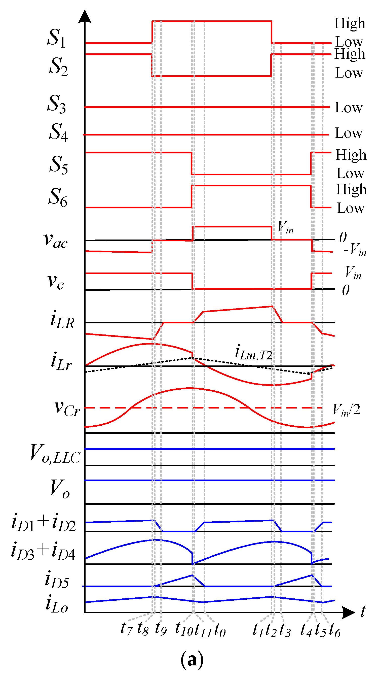
When Vin is in the high voltage region (Vin,L = 270 V–600 V), Q is turned on and S3 and S4 are turned off. Switches S1, S2, S5, and S6 and passive components T1, LR, D1, D2, and Lo are controlled by phase shift PWM scheme. Components S5, S6, T2, Lr, Cr, D3, D4, and CLLC are operated as the LLC resonant circuit to have ZVS operation of S5 and S6. The turns ratio of full bridge converter under the high input-voltage region is 2np1/ns1 in Figure 2b. Figure 4a shows PWM waveforms for high voltage input region. Figure 4b–g provides the equivalent state circuits for first half switching period.
State 1 [t0t < t1]: In this state, switches S1 and S6 are ON and the leg voltage vac = Vin. LLC converter (S6, Lr, T2, Cr, D4, and CLLC) is operated at the resonant frequency. On the secondary side, D1 and D4 are conducting. The drain voltages vCS2 = vCS5 = Vin and the diode voltage stresses vD2Vinns1/np1 and vD3 ≈ 2Vo,LLC. The inductor currents iLo and iLR are increased and iLr is decreased in this state.
State 2 [t1t < t2]: At t1, switch S1 is turned off. Owing to iLR(t1) > 0, iLR discharges CS2. If the inductor energy [ L R + ( 2 n p 1 / n s 1 ) 2 L o ] i L R 2 ( t 1 ) > 2 C o s s V i n 2 , then CS4 can be completely discharged to zero voltage.
State 3 [t2t < t3]: At t2, vCS2 = 0. Since iLR(t2) > 0, DS2 conducts and S2 is turned on at ZVS. In this state, the leg voltage vac = 0 so that D5 is forward biased. Therefore, the rectified voltage VR = Vo,LLC, vLR = −2 × np1Vo,LLC/ns1 < 0 and vLo = Vo,LLCVo < 0. The inductor currents iLr, iLo, and iLR are all decreased in state 3. If the primary currents iLR or iD1 can be declined to zero, then the necessary time interval of the freewheeling state at the high input-voltage region is derived as:
Δ t i L R = 0 L R I o / [ ( 2 n p 1 / n s 1 ) 2 V o , L L C )
If iD1 = 0 at t3, then the circuit operation goes to state 4. If iD1 is not equal to zero at the end of the freewheeling state, then the circuit goes to state 5.
State 4 [t3t < t4]: At t3, iD1 = 0. One can observe iD5 = iLo and the primary current iLR is approximately equal to zero when vac = 0 (freewheeling state). Since D5 is conducting, power is delivered to Vo through LLC resonant converter in state 4.
State 5 [t4t < t5]: At t4, S6 turns off. Owing to iLR(t4) − iLr(t4) > 0, CS5 will be discharged. In LLC circuit, D3 is conducting. At t5, vCS5 is decreased to zero voltage.
State 6 [t5t < t6]: At t5, vCS5 = 0. Owing to iLR(t5) − iLr(t5) > 0, DS5 is conducting. Thus, S5 is turned on at ZVS. In state 6, vac = −Vin and D2 is forward biased. Due to iD2(t5) < iLo(t5), D5 is still conducting and VR = Vo,LLC. The primary inductor voltage vLR ≈ 2np1Vo,LLC/ns1Vin < 0 and iLR decreases. At the end of state 6, the diode current iD2 = iLo so that D5 is conducting. The duty loss at state 6 under the high input-voltage region is obtained as:
d 6 f s w I o L R / [ 2 n p 1 ( V i n 2 n p 1 V o , L L C / n s 1 ) / n s 1 ]
At time t6, the converter goes to the next half switching period.

4. Circuit Characteristics

A three-leg full bridge circuit and a LLC resonant circuit are included in the studied converter. Both PWM circuit and LLC circuit will achieve power transfer from Vin to Vo. LLC circuit is controlled at constant frequency. Thus, the secondary-side voltage Vo,LLC is calculated in (11):
V o , L L C = V i n n s 2 / ( 2 n p 2 )
At the freewheeling state, the primary-side leg voltage vac or vbc is zero and diode D5 is forward biased. Thus, the rectifier terminal voltage VR = Vo,LLC. The primary inductor voltage vLR= −np1Vo,LLC/ns1 (low input-voltage region) or vLR= −2 × np1Vo,LLC/ns1 (high input-voltage region) and the primary current iLR will decrease to zero at the freewheeling state. Due to LLC circuit is controlled under the inductive impedance, S5 and S6 can turn on at zero voltage. Due to voltage-second balance on Lo, Vo is derived in (2).
V o = k d e f f V i n n p 1 / n s 1 + ( 1 2 d e f f ) V i n 2 n p 2 / n s 2
deff is the effective duty cycle and k = 1 (or 2) under the high (or low) input-voltage region. From Equation (12), the proposed converter has a voltage gain as Equation (13).
G d c , p r o p o s e d = V o V i n = k d e f f n p 1 / n s 1 + ( 1 2 d e f f ) 2 n p 2 / n s 2
If the proposed converter does not use LLC resonant circuit at lagging-leg (S5 and S5), then the voltage gain of three-leg converter without LLC converter is derived as:
G d c , c o n = V o V i n = k d e f f n p 1 / n s 1
The voltage gains of the presented circuit and conventional PWM converter are compared and provided as:
G d c , p r o p o s e d G d c , c o n = 1 + n p 1 ( 1 2 d e f f ) / n s 1 2 n p 2 k d e f f / n s 2 > 1
From Equation (15), the presented circuit has a much larger voltage gain. The power ratings of LLC circuit and full bridge circuit in the presented converter are given as:
P L L C = ( 1 2 d e f f ) V o . L L C I o ( 1 2 d e f f ) V i n I o / ( 2 n p 2 / n s 2 )
P f u l l b r i d g e = 2 d e f f V i n I o n p 1 / n s 1
In steady state, the ripple currents ΔiLo of conventional PWM converter and the presented converter are expressed as
Δ i L o , c o n > V o ( 0.5 d e f f ) L o f s w
Δ i L o , p r o p o s e d ( V o V o , L L C ) ( 0.5 d e f f ) L o f s w
From Equations (18) and (19), the ripple current comparison is given as.
Δ i L o , p r o p o s e d Δ i L o , c o n = 1 V o , L L C / V o < 1
That means the presented converter has less ripple current ΔiLo. The voltage ratings of S1S6 and Q are equal to Vin,max. The voltage rating of D1 and D2 is approximately equal to Vin,max/(np1/ns1). Similarly, the voltage rating of D3 and D4 is approximately equal to Vin,max/(np2/ns2). The voltage stress of D5 is Vin,max/(np1/ns1) − Vin,max/(np2/ns2). The DC diode currents of D1D5 are I D 1 = I D 2 d e I o , I D 3 = I D 4 ( 0.5 d e ) I o and I D 5 ( 1 2 d e ) I o .

5. Experimental Results

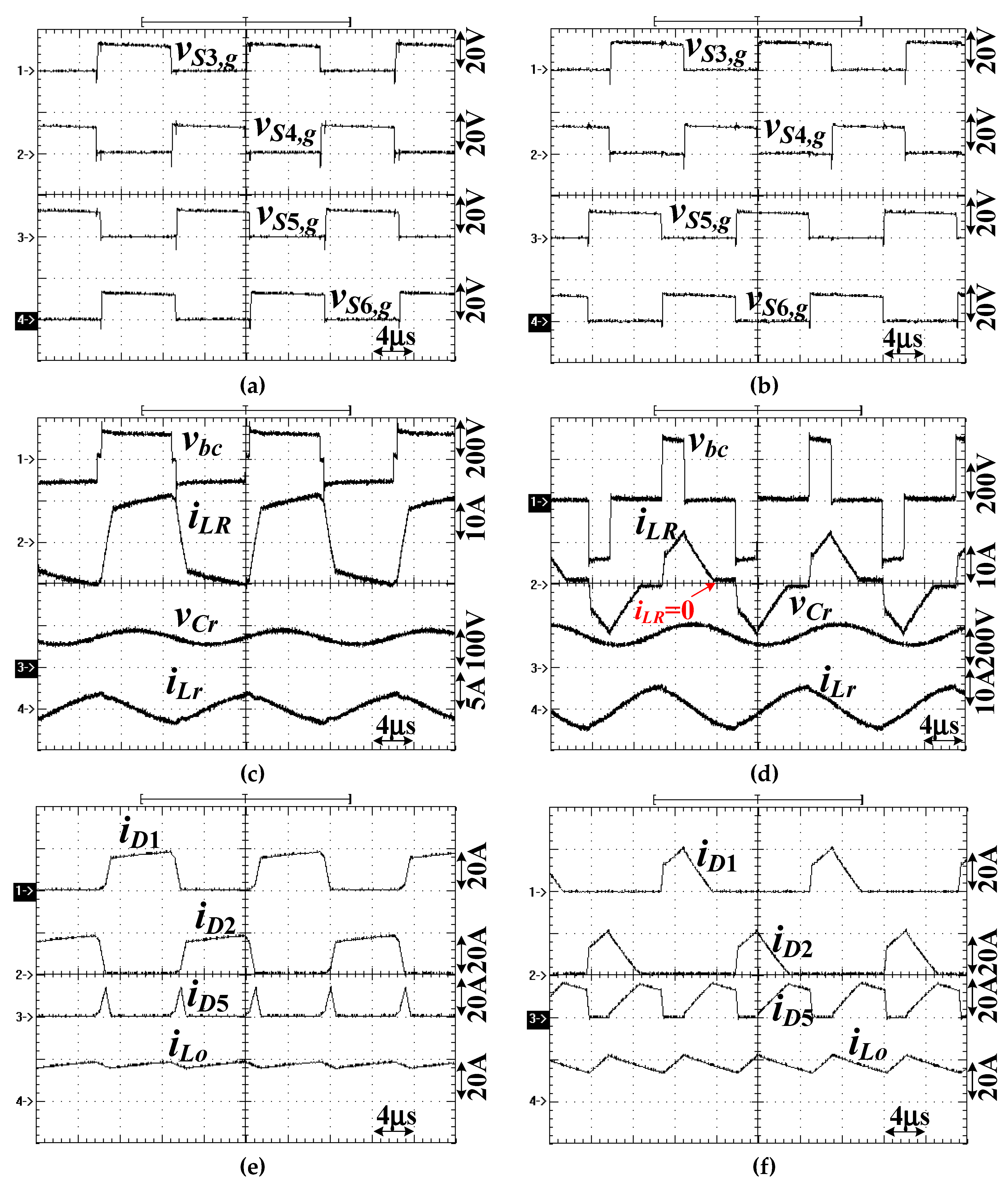
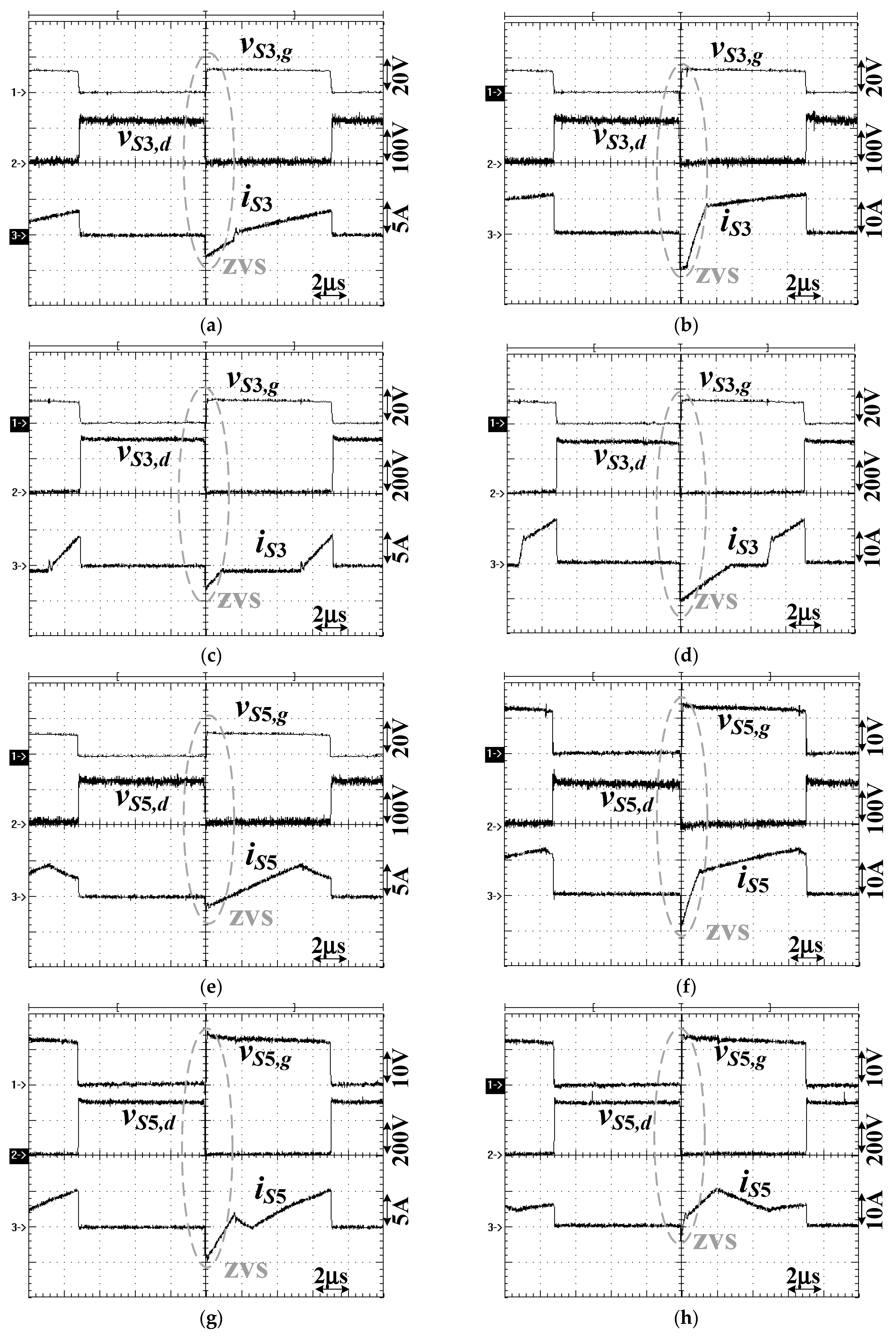
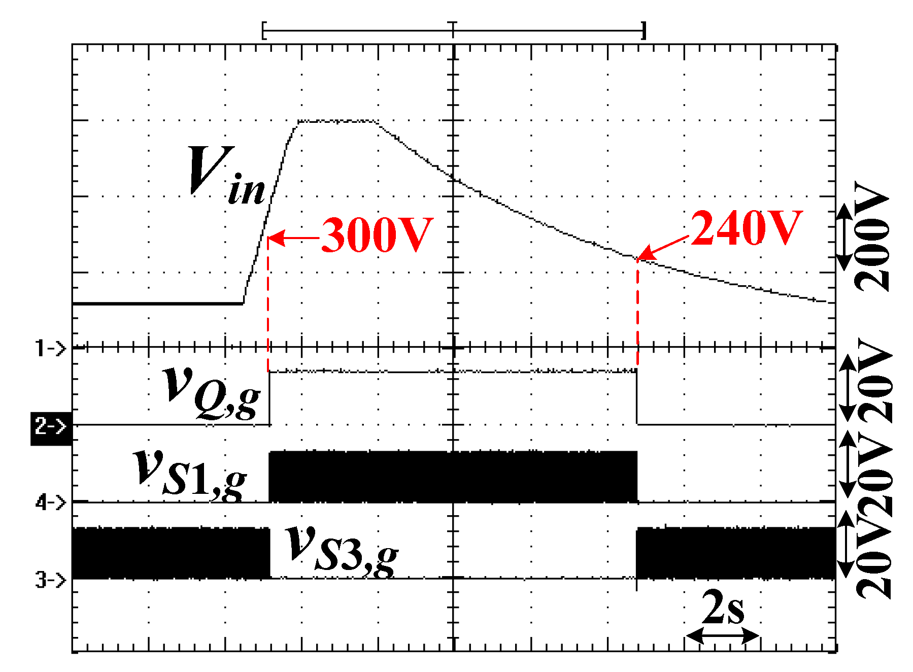
The laboratory prototype with a rated power Po = 800 W is built and tested. The circuit components of the laboratory prototype are provided in Table 1. Figure 5 gives the control block of the studied converter. The general purpose PWM integrated circuit UCC3895 is selected to generate the necessary PWM waveforms to drive the leading and lagging leg switches. A comparator with ±30 V voltage tolerance is adopted in control block to decide low voltage input or high voltage input range. The reference voltage of Schmitt voltage comparator is designed at 270 V. Thus, the actual low and high voltage input ranges are Vin,L=120–300 V and Vin,H = 240–600 V. Figure 6 gives the experimental test bench. The digital oscilloscope Tektronix TDS3014B, the dc electronic load Chroma 63112A, and the dc power source Chroma 62016P-600-8 are used in the laboratory test to measure the experimental results. Figure 7 provides the experimental results at the low voltage region (Vin,L = 120–300 V) and full load. Figure 7a,b gives the experimental PWM signals of S3~S6 for 120 and 300 V, respectively. The leg voltage vbc, primary currents iLR and iLr, and resonant voltage vCr under 120 V input case are provided in Figure 7c. Similarly, the measured waveforms of vbc, iLR, iLr, and vCr under 300 V input case are shown in Figure 7d. Comparing Figure 7c,d, the leg voltage vbc at Vin = 300 V has less duty ratio. Since the secondary-side voltage Vo,LLC is connected to the rectified terminal VR, the inductor voltage vLR at the circulating state is negative and iLR will decrease to zero in this state. Figure 7e,f demonstrates the measured waveforms of iD1, iD2, iD5, and iLo for Vin = 120 and 300 V cases. One can observe that the PWM converter has less duty cycle and more ripple current ΔiLo on Lo under Vin = 120 V input case in Figure 7d,f. Figure 8a provides the PWM signals of S3 (the leading-leg switch) at Vin = 120 V input and Po = 20% rated load. In the same manner, the measured PWM waveforms of S3 at Vin = 120 V input and Po = 100% rated load are provided in Figure 8b. Figure 8c,d illustrates the test waveforms of S3 under Vin = 300 V input and 20% and 100% rated loads, respectively. The PWM waveforms of S5 for different input voltages (Vin = 120 and 300 V) and different loads (20% and 100% loads) are provided in Figure 8e–h. From Figure 8, it is clear that active switches S3 and S5 can both turn on at ZVS for 120 and 300 V input cases. Likewise, the test waveforms at high voltage input (Vin = 240–600 V) and the rated power are given in Figure 9. Since S3 and S4 are off under high voltage input condition, only PWM waveforms of S1, S2, S5, and S6 are shown in Figure 9a,b for 240 and 600 V, respectively. The measured leg voltage vac, primary currents iLR and iLr and resonant voltage vCr for 240 and 600 V inputs are given in Figure 9c,d, respectively. It can be noted in Figure 9d, iLR will decrease to zero during the circulating interval. The experimental waveforms of iLo, iD5, iD2, and iD1 for Vin = 240 and 600 V are illustrated in Figure 9e,f. The hysteresis voltage comparator is used in the control block and the reference voltage is designed at 270 V with ±30 V voltage tolerance. Figure 10a,b shows the PWM signals of S1 under 240 V input and different load conditions (20% and 100% rated loads). Figure 10c,d provides the test waveforms of S1 under 600 V input and different loads (20% and 100% loads). The PWM signals of S5 at different input voltages (Vin = 240 and 600 V) and different load conditions (20% and 100% loads) are provided in Figure 10e–h. It can be noted that S1 and S5 all turn on under zero voltage. Figure 11 gives the test PWM waveforms of Q, S1, and S3 during the input voltage variation between Vin = 120 and 600 V. When Vin increases from 120 to 600 V, Q turns on and S3 turns off at Vin = 300 V. At the same time, S1 is activated at Vin > 300 V. On the other hand, Q and S1 turn off and S3 is activated at Vin = 240 V when Vin decreases from 600 to 120 V. The measured efficiencies of the proposed converter at the rated power are 89.7%, 91.2%, 90.9%, and 93.4% under Vin = 120, 240, 300. and 600 V, respectively. Using thermal imaging camera FLIR E85, the measured junction and case temperatures of power MOSFET S5 at the rated power are 98 °C and 85 °C. The junction and case temperatures of rectifier diode D1 are 102 °C and 90 °C. The measured core and winding temperatures of filter inductor Lo with MPP core CM343125 are 87 °C and 82 °C, respectively, at the rated power.

6. Conclusions

A hybrid PWM converter is presented and investigated to achieve wide voltage operation (Vin = 120–600 V), ZVS operation for all active devices and low primary current loss at the freewheeling state. To solve high circulating current drawback in conventional full bridge converter, a DC voltage comes from a LLC circuit is used at the secondary rectified terminal. Thus, the primary inductor voltage is negative and the circulating current will reduce to zero during freewheeling state. The other drawback of conventional PWM converter is serious switching loss on lagging leg devices. The added LLC circuit shares the same lagging-leg devices as PWM circuit to help the lagging-leg active devices to be turned on at zero voltage. Three-leg PWM circuit structure is used to achieve wide voltage input operation. The circuit performance is provided through the experimental results.

Author Contributions

Conceptualization, methodology, investigation, visualization, writing—original draft, writing—review and editing, B.-R.L.; validation, Y.-C.L. All authors have read and agreed to the published version of the manuscript

Funding

This research is supported by the Ministry of Science and Technology (MOST), Taiwan, under grant number MOST 108-2221-E-224-022-MY2.

Acknowledgments

The authors are grateful to the all the editor and the reviewers for their valuable suggestions to improve this paper.

Conflicts of Interest

The authors declare no conflict of interest.

References

  1. Tahir, S.; Wang, J.; Baloch, M.H.; Kaloi, G.S. Digital Control Techniques Based on Voltage Source Inverters in Renewable Energy Applications: A Review. Electronics 2018, 7, 18. [Google Scholar] [CrossRef] [Green Version]
  2. Almalaq, Y.; Matin, M. Three topologies of a non-isolated high gian switched-capacitor step-up cuk converter for renewable energy applications. Electronics 2018, 7, 94. [Google Scholar] [CrossRef] [Green Version]
  3. Blaabjerg, F.; Dragicevic, T.; Davari, P. Applications of Power Electronics. Electronics 2019, 8, 465. [Google Scholar] [CrossRef] [Green Version]
  4. Kim, J.-Y.; Kim, H.-S.; Baek, J.-W.; Jeong, D.-K. Analysis of Effective Three-Level Neutral Point Clamped Converter System for the Bipolar LVDC Distribution. Electronics 2019, 8, 691. [Google Scholar] [CrossRef] [Green Version]
  5. Steigerwald, R.L. A comparison of half-bridge resonant converter topologies. IEEE Trans. Power Electron. 1988, 3, 174–182. [Google Scholar] [CrossRef]
  6. Lin, B.-R.; Dai, C.-X. Wide Voltage Resonant Converter Using a Variable Winding Turns Ratio. Electronics 2020, 9, 370. [Google Scholar] [CrossRef] [Green Version]
  7. Ren, R.; Liu, B.; Jones, E.A.; Wang, F.F.; Zhang, Z.; Costinett, D. Capacitor-clamped, three-level Gan-based dc-dc converter with dual voltage outputs for battery charger applications. IEEE J. Emerg. Sel. Top. Power Electron. 2016, 4, 841–853. [Google Scholar] [CrossRef]
  8. Safaee, A.; Jain, P.; Bakhshai, A. A ZVS Pulsewidth Modulation Full-Bridge Converter with a Low-RMS-Current Resonant Auxiliary Circuit. IEEE Trans. Power Electron. 2015, 31, 4031–4047. [Google Scholar] [CrossRef]
  9. Wang, X.; Tian, F.; Batarseh, I. High Efficiency Parallel Post Regulator for Wide Range Input DC–DC Converter. IEEE Trans. Power Electron. 2008, 23, 852–858. [Google Scholar] [CrossRef]
  10. Wu, H.; Wan, C.; Sun, K.; Xing, Y. A High Step-Down Multiple Output Converter with Wide Input Voltage Range Based on Quasi Two-Stage Architecture and Dual-Output LLC Resonant Converter. IEEE Trans. Power Electron. 2015, 30, 1793–1796. [Google Scholar] [CrossRef]
  11. Lin, B.-R.; Hsieh, F.-Y. Soft-Switching Zeta–Flyback Converter with a Buck–Boost Type of Active Clamp. IEEE Trans. Ind. Electron. 2007, 54, 2813–2822. [Google Scholar] [CrossRef]
  12. Jeong, Y.; Park, J.D.; Moon, G.-W. An Interleaved Active-Clamp Forward Converter Modified for Reduced Primary Conduction Loss Without Additional Components. IEEE Trans. Power Electron. 2019, 35, 121–130. [Google Scholar] [CrossRef]
  13. Lin, B.-R.; Chao, C.-H. A New ZVS DC/DC Converter with Three APWM Circuits. IEEE Trans. Ind. Electron. 2012, 60, 4351–4358. [Google Scholar] [CrossRef]
  14. Pont, N.C.D.; Bandeira, D.; Lazzarin, T.B.; Barbi, I. A ZVS APWM half-bridge parallel resonant DC–DC converter with ca-pacitive output. IEEE Trans. Ind. Electron. 2019, 66, 5231–5241. [Google Scholar] [CrossRef]
  15. Lin, B. Resonant converter with wide input voltage range and input current ripple-free. Electron. Lett. 2018, 54, 1086–1088. [Google Scholar] [CrossRef]
  16. Wang, P.; Zhou, L.; Zhang, Y.; Li, J.; Sumner, M. Input-Parallel Output-Series DC-DC Boost Converter with a Wide Input Voltage Range, For Fuel Cell Vehicles. IEEE Trans. Veh. Technol. 2017, 66, 7771–7781. [Google Scholar] [CrossRef]
  17. Hu, H.; Fang, X.; Chen, F.; Shen, Z.J.; Batarseh, I. A Modified High-Efficiency LLC Converter with Two Transformers for Wide Input-Voltage Range Applications. IEEE Trans. Power Electron. 2013, 28, 1946–1960. [Google Scholar] [CrossRef]
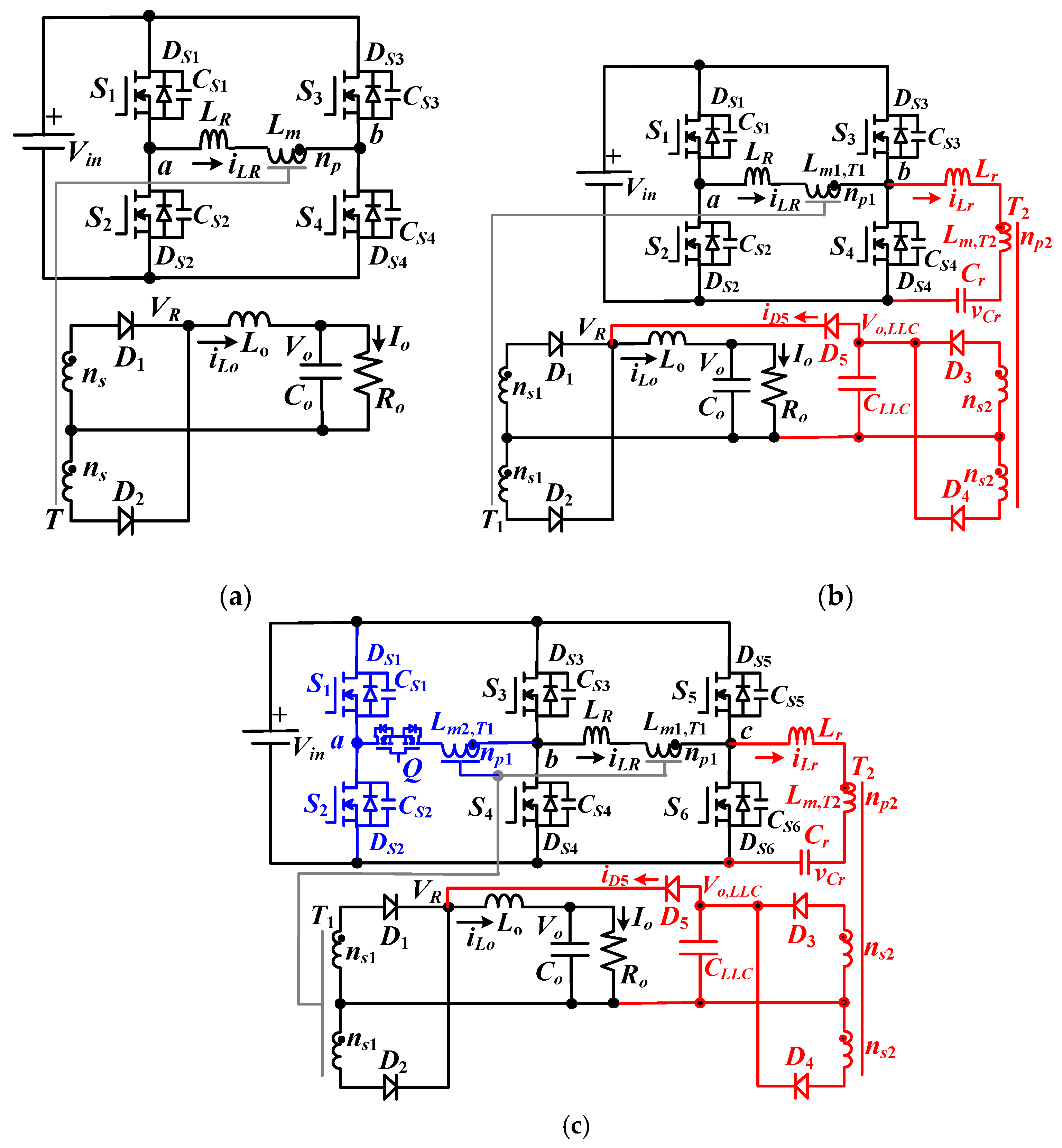
Figure 1. Circuit structure (a) conventional phase-shift PWM converter, (b) hybrid soft switching PWM converter with less primary current at the freewheeling state, (c) proposed hybrid soft switching PWM converter with wide input voltage operation and less primary current at the freewheeling state.
Electronics 10 00473 g001
Figure 2. Proposed hybrid PWM converter (a) operated at low voltage operation, 120 V ≤ Vin < 270 V, (b) operated at high voltage operation, 270 V < Vin ≤ 600 V.
Electronics 10 00473 g002
Figure 3. Low input-voltage region operation (a) PWM waveforms, (b) state 1, (c) state 2, (d) state 3, (e) state 4, (f) state 5, (g) state 6.
Electronics 10 00473 g003aElectronics 10 00473 g003b
Figure 4. High input-voltage region operation (a) PWM waveforms, (b) state 1, (c) state 2, (d) state 3, (e) state 4, (f) state 5, (g) state 6.
Electronics 10 00473 g004aElectronics 10 00473 g004b
Figure 5. Control block of the laboratory prototype.
Electronics 10 00473 g005
Figure 6. Pictures of the proposed converter in the laboratory: (a) Prototype circuit, (b) experimental setup.
Electronics 10 00473 g006
Figure 7. Measured PWM signals at full load and low input-voltage range (a) S3 ~ S6 at Vin = 120 V, (b) S3 ~ S6 at Vin = 300 V, (c) vbc, iLR, vCr, iLr at Vin = 120 V, (d) vbc, iLR, vCr, iLr at Vin = 300 V, (e) iD1, iD2, iD5, iLo at Vin = 120 V, (f) iD1, iD2, iD5, iLo at Vin = 300 V.
Electronics 10 00473 g007
Figure 8. Measured PWM waveforms of S3 and S5 at the low input-voltage region (a) S3 at Vin = 120 V and Po = 20% load, (b) S3 at Vin = 120 V and Po = 100% load, (c) S3 at Vin = 300 V and Po = 20% load, (d) S3 at Vin = 300 V and Po = 100% load, (e) S5 at Vin = 120 V and Po = 20% load, (f) S5 at Vin = 120 V and Po = 100% load, (g) S5 at Vin = 300 V and Po = 20% load, (h) S5 at Vin = 300 V and Po = 100% load.
Electronics 10 00473 g008
Figure 9. Measured PWM signals at full load and high input-voltage range (a) S1, S2, S5, S6 at Vin = 240 V, (b) S1, S2, S5, S6 at Vin = 600 V, (c) vac, iLR, vCr, iLr at Vin = 240 V, (d) vac, iLR, vCr, iLr at Vin = 600 V, (e) iD1, iD2, iD5, iLo at Vin = 240 V, (f) iD1, iD2, iD5, iLo at Vin = 600 V.
Electronics 10 00473 g009
Figure 10. Measured PWM waveforms of S1 and S5 at the high input-voltage region (a) S1 at Vin = 240 V and Po = 20% load, (b) S1 at Vin = 240 V and Po = 100% load, (c) S1 at Vin = 600 V and Po = 20% load, (d) S1 at Vin = 600 V and Po = 100% load, (e) S5 at Vin = 240 V and Po = 20% load, (f) S5 at Vin = 240 V and Po = 100% load, (g) S5 at Vin = 600 V and Po = 20% load, (h) S5 at Vin = 600 V and Po = 100% load.
Electronics 10 00473 g010
Figure 11. Measured waveforms of Vin, Q, S1 and S3 between 120 and 600 V input condition.
Electronics 10 00473 g011
Table 1. Circuit parameters in the laboratory prototype.
ItemsParameterItemsParameter
Vin120–600 VLo30 μH
Vo48 VS1~S6, QSTF15N95K5
Po800 WD1~D4MBR40500PT
fsw70 kHzD5STTH2003CT
Co640 μF/100 Vnp1:ns116:10
Co,LLC240 μF/100 Vnp2:ns222:2
Cr205 nFLm1,T1, Lm2,T1259 μH
Lr27 μHLm,T2135 μH
Publisher’s Note: MDPI stays neutral with regard to jurisdictional claims in published maps and institutional affiliations.