Abstract
Because modern electronic systems are likely to be exposed to high intensity radiated fields (HIRF) environments, there is growing interest in understanding how electronic systems are affected by such environments. Backdoor coupling in particular is an area of concern for all electronics, but there is limited understanding about the mechanisms behind backdoor coupling. In this work, we present a study on printed circuit board (PCB) backdoor coupling and the effects of via fencing. Existing work focuses on ideal stackups and indicates that edge radiation is significantly reduced by via fencing. In this study, both full wave electromagnetic modeling and experimental verification are used to investigate both ideal and practical PCB stackups. In the ideal scenario, we find that via fencing substantially reduces coupling, which is consistent with prior work on emissions. In the practical scenario, we incorporate component footprints and traces which naturally introduce openings in the top ground plane. Both simulation and experimental data indicate that via fencing in the practical scenario does not substantially mitigate coupling, suggesting that PCB edge coupling is not the dominant coupling mechanism, even at varying angles of incidence and polarization.
1. Introduction
In recent years, there has been growing concern about the effects of high intensity radiated fields (HIRF) environments on electronic devices and systems. These high-intensity fields are generated by various sources including high-power long-range communication antennas as well as directed energy weapons—sometimes referred to as intentional electromagnetic interference (IEMI) sources. Naturally, this concern encompasses both civilian and military applications. As a result, the Federal Aviation Administration (FAA) and the Department of Defense (DoD) have taken action to implement hardening requirements and develop a better understanding of how HIRF environments affect electronic devices [1,2,3,4,5,6,7,8].
These standards as, well as other reports, indicate that typical field strengths encountered in HIRF environments can reach tens of kilovolts per meter ( 10 /) [9,10,11]. As will be shown in the results presented here, a field strength of this magnitude can easily generate an induced voltage of 10 or more, which is certainly concerning for modern electronics that typically operate with a 5 or supply voltage. Furthermore, supply voltages are constantly trending downward in order to meet power and thermal requirements for various applications, which naturally exacerbates this problem further.
Due to the complexity of modern electronic systems, this problem has been studied at various subsystem levels ranging from components [9,12,13,14] and printed circuit boards (PCB) [15,16,17,18,19,20] to cables [21,22,23,24,25,26,27] and enclosures [15,25,26,27,28,29,30], with some groups even considering the system as a whole [31]. Furthermore, this problem is typically separated into four areas of study: coupling, energy distribution, device response, and system response.
This work focuses specifically on the coupling area of study, which is typically divided into two primary categories of interest, namely front door coupling and backdoor coupling. Front door coupling refers to coupling to intentional antennas, whereas backdoor coupling refers to coupling to unintentional antennas including wires, cables, PCB traces and planes, and component bondwires. The intention behind this work is to provide a better understanding of the mechanisms behind backdoor coupling at the PCB level and the major parameters that might affect the degree of coupling. Such information could lead to the development of mitigation techniques that would decrease coupling in HIRF environments and reduce the risk of system interruption or damage.
The study presented here provides insight into PCB power and ground plane coupling and the effects of via fencing. To our knowledge, there has been very little investigation into PCB coupling in general, with related work focusing primarily on PCB emissions. Emissions studies are certainly complementary to radiated susceptibility studies due to the principle of reciprocity, but care should be taken to avoid directly applying conclusions from one domain to the other.
Prior to discussing the existing literature on this topic, it is important to clarify terminology to avoid confusion. Throughout this paper, the term “via stitching” will be used to refer to vias throughout the inner area of a PCB, while “via fencing” will be used to refer to vias around the perimeter of a PCB. Sparse via stitching occurs naturally in multilayer PCBs when grounding various component pads, but in some cases, additional via stitching is implemented in order to maintain low ground plane impedance and shorten return paths [32]. It is also worth noting that the term “via shielding” sometimes refers to surrounding specific traces with grounding vias to reduce crosstalk [33,34,35].
Among the existing literature, there is a substantial amount of research involving the reduction in emissions from a PCB using several different techniques. For example, the 20H rule is a commonly referenced rule of thumb whereby the power plane is pulled back from the PCB edge by a factor of twenty times the dielectric thickness [36,37,38,39,40,41,42,43,44,45]. There is substantial debate over whether this method does or does not reduce emissions, suggesting that the answer depends on other factors, such as the PCB stackup. Others have investigated via fencing around the PCB perimeter in order to form a pseudo Faraday cage [36,38,46,47,48,49,50,51]. Furthermore, some groups have investigated more advanced techniques including edge plating [36,38] and the incorporation of electromagnetic bandgap structures [52].
In addition to focusing on emissions, many of the existing studies present results based on ideal PCB stackups [36,37,38,46,47,50,51,53]. In other words, the existence of traces and vias that result in discontinuous planes is not considered. Such approaches are not without merit, but the conclusions drawn from prior work may not necessarily apply to practical stackups and layouts.
Thus, the contributions of this work are twofold. First, this work provides a novel investigation into the radiated susceptibility of PCBs and the effects of via fencing. Second, in order to understand the implications of practical PCB stackups, this work provides a comparison between ideal and practical scenarios, which has not been done by the prior work cited here. This comparison is critical because it provides insight into whether or not via fencing plays a substantial role in mitigating coupling in a realistic scenario.
This work is organized as follows. Section 2 provides a discussion on the theory behind power plane resonance and traditional via fencing approaches. In Section 3, the modeling and experimental methods used in this work are described in detail. Section 4 provides a combination of simulated and experimental data for an ideal multilayer PCB and a practical multilayer PCB. Lastly, Section 5 offers further discussion on the results and provides plans for future work.
2. Theory
2.1. Plane Coupling Theory
When a plane wave is incident on a PCB, it excites resonant modes on the planes and traces based on the geometry and dielectric material of the PCB. In particular, the PCB power and ground planes effectively form a dielectric loaded cavity or parallel plate waveguide [15,23,30,36,54,55,56]. The resonant frequencies () of an ideal parallel plate waveguide can be calculated by considering the transverse magnetic () modes as follows:
where subscripts m and n are the mode indices, c is the speed of light, is the relative permittivity of the substrate, and a and b are the length and width of the plates, respectively. In general, for a 3D rectangular cavity, this equation would normally include a third term associated with the height of the cavity. However, in practical PCBs, the vertical distance between the planes is much smaller than the wavelengths of interest, and thus such modes can be ignored. It should be noted that this equation is for ideal parallel plates and does not directly extend to the multi-layer PCB structures studied here. For such multi-layered structures, as well as non-rectangular PCBs, eigenvalue analysis is typically employed to determine resonant modes [23].
As an example, Figure 1 shows the electric field pattern for multiple resonant frequencies including the fundamental and modes as well as higher order modes that can be excited in an ideal PCB structure. Note that because the electric field intensity varies across the power plane, the measured induced voltage also varies. In fact, at the nodes of the standing wave patterns (blue regions in the plots), the induced voltage is minimal.

Figure 1.
Electric field patterns for a sample of transverse magnetic (TM) resonant modes within a four-layer printed circuit board (PCB): (a) , (b) , (c) , and (d) .
2.2. Via Fencing Theory
Most modern PCBs have at least four layers with a typical stackup including external signal layers and internal power and ground planes. Components are also usually placed on both sides of the board to reduce board size and maximize layout efficiency. As a result, signals between components typically transition between signal layers using signal vias.
As mentioned previously, by leveraging the principle of reciprocity, it can be helpful to consider this scenario first from an emissions perspective. As current travels through these signal vias, radially propagating waves are generated within the power and ground planes, which effectively behave as a parallel plate waveguide [36,37,49]. When these waves reach the perimeter of the board, some of the energy is reflected due to impedance mismatch, while some of the energy is radiated away from the board.
The existing literature suggests that via fencing as well as plating around the perimeter of the board cause greater reflections within the PCB and therefore reduce radiation. Thus, it seems that via fencing and other edge treatment techniques may also mitigate coupling to the power and ground planes from an external plane wave. This work addresses this question directly.
3. Materials and Methods
Both modeling and experimental procedures were used to investigate the effectiveness of via fencing in reducing coupling to the PCB planes. Each of the tested PCBs were designed to be identical except for the via fencing density along the perimeter. A single surface mount sub-miniature version A (SMA) connector was used to make measurements of the power plane voltage in a controlled manner. To ensure that the simulation captured the experimental setup closely, the SMA connector was also included in the model.
3.1. Full Wave Modeling
Each design in this study was simulated using Ansys High Frequency Structure Simulator (HFSS), which is a full-wave electromagnetic simulation application. The PCB designs were excited using a plane wave with a 1 / electric field strength. When reviewing the data, it should be noted that a field strength of 1 / was only used for convenience here and naturally yielded induced voltages that were quite low—in the order of millivolts in the worst case. However, when these voltages are scaled to reflect the typical field strengths encountered in HIRF environments, they can easily reach levels that cause disruption and even permanent damage, as discussed previously.
A perfectly matched layer (PML) boundary condition was also used to emulate free space conditions, and a lumped port was used as the load with an impedance of 50 . For the ideal stackup, the port was placed between the inner power and ground planes, while for the practical stackup, the port was placed at the end of an SMA connector (see Section 4 for model figures). Each model was analyzed using a frequency domain simulation with a frequency range of 0.1 to 10 .
To measure the induced voltage at the port, a line was placed at the center of the port between the two conductors. The complex voltage phasor was then calculated by integrating the electric field along this path:
where is the complex voltage drop as defined in HFSS and l is the path along which the field is integrated. This quantity is calculated at each frequency in the sweep. Because phase is not critical in this analysis, the plots shown here are generated by taking the magnitude () of the complex voltage:
In order to improve the accuracy of this calculation, an additional meshing operation was implemented on the surface of the lumped port. The meshing operation was set to generate at least twenty meshing elements along the path to be integrated. Furthermore, the voltage quantity () was used as an additional convergence criterion in the HFSS adaptive meshing procedure to ensure the accuracy of the results.
3.2. Experimental Procedure
Experiments were conducted to compare the results of the HFSS simulations to the physical test articles. Each device under test (DUT) was placed in an anechoic chamber (Model 5247, ETS-Lindgren, Cedar Park, TX, USA) and illuminated by an ultra-broadband 750 –18 horn antenna (Model 3115, ETS-Lindgren, Cedar Park, TX, USA). The horn antenna was fed a single-tone sinusoidal signal generated by a high frequency 25 arbitrary waveform generator (AWG) (Model M8195A, Keysight, Santa Rosa, CA, USA) and amplified by an 8 wideband 1–22 power amplifier (Model RFLUPA01G22GA, RF-Lambda, Carrollton, TX, USA). The measurements were obtained using an 8 mixed signal oscilloscope (Model WavePro 804-HD, Teledyne LeCroy, Chestnut Ridge, NY, USA). Although simulations were performed with a frequency range of 0.1 to 10 , the experimental setup was limited to a frequency range of 1 to 8 . The overall experimental setup, including all equipment and fixtures, is shown in Figure 2.
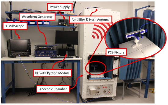
Figure 2.
Experimental setup loop for making controlled induced voltage measurements. Signal generation is performed using a waveform generator, power supply, amplifier, and horn antenna. An anechoic chamber is used to mimic free-space conditions in a controlled environment, and a fixture is used for holding the device under test (DUT) at a consistent location and in a consistent orientation. Voltage measurements are performed using an oscilloscope, and a PC with a custom Python module is used to automate the testing procedure.
In order to compare experimental voltages to simulated voltages, it was first necessary to determine the electric field strength at the DUT. The electric field strength can then be used to normalize and scale the experimental measurements for direct comparison to the simulation results. To determine the electric field strength, an extensive characterization of the chamber and testing loop was performed.
In the following derivation, some of the quantities are relative and include associated units in square brackets. Quantities without units, on the other hand, are absolute. Preference is given to relative quantities throughout the derivation because they simplify the calculation considerably. Recall that absolute voltage and power quantities can be converted to relative quantities with the log function, as shown in the following equations:
where is the power expressed in decibels relative to one watt and is the voltage expressed in decibels relative to one volt.
To characterize the chamber, a second horn antenna was first placed on the test article platform in the anechoic chamber. A vector network analyzer (VNA) (Model C2420, Copper Mountain, Indianapolis, IN, USA) was then used to measure scattering parameters for the two-port network created by the horn antennas. In particular, port 1 was connected to the amplifier and port 2 was connected to the second horn antenna. Scattering parameter in this scenario reflects the change in power received after passing through the cabling, the amplifier, the transmitting antenna, the free space region of the chamber, and the receiving antenna. It effectively relates the transmitted power () to the received power ():
We can now relate the received power to the peak output voltage using basic circuit theory:
where and are the RMS and peak output voltages, respectively. We then modify this equation to use relative quantities using Equations (4) and (5):
Combining Equation (6) with Equation (10) and solving for provides a relationship between the output voltage, the transmitted power, and the forward voltage gain scattering parameter:
Now, the final step is to relate the output voltage to the incident electric field, which can be done with basic antenna theory. In particular, the antenna factor () is a quantity that directly relates the voltage () at the antenna port to the electric field strength (E) at the phase center of the antenna:
Note that the antenna factor is a quantity measured by the manufacturer after characterizing a given horn antenna. This information was provided upon request.
After inserting Equation (11) into Equation (12) and solving for , we are able to determine the power required to generate a desired field strength at the DUT:
This quantity is then used to set the waveform amplitude. The current setup is able to generate field strengths at the DUT in excess of 30 /.
A Python module was developed to automate the experimental testing procedure. The module obtains user input for the desired frequency range and field strength at the DUT. The module then controls the AWG for signal generation and oscilloscope for signal measurement.
For each test frequency, the Python module performs the following steps:
- Uses Equation (13) to determine the required transmitted power to produce the desired field strength for a given frequency;
- Communicates with the AWG component object model (COM) driver and generates a single-tone sinusoidal waveform with peak-to-peak voltage determined in the first step;
- Communicates with the oscilloscope and commands it to wait for the signal to settle and then measure the peak-to-peak voltage of the output signal;
- De-embeds the frequency response of the output cabling and the oscilloscope;
- Normalizes the compensated output response to the field strength defined by the user;
- Stores the frequency and normalized voltage measurement.
Once the test process has been conducted for the entire frequency range, the module exports a CSV file containing each normalized induced voltage measurement and its corresponding frequency for the whole test frequency range.
4. Results
4.1. Radiated Susceptibility of Ideal Multilayer PCB
We begin with an ideal multilayer PCB which does not contain pads, traces, or vias as shown in Figure 3. Figure 4 also shows the stackup of the PCB including the thickness of each layer. FR4 was used as the dielectric substrate with a nominal permittivity of 4.27. Note that this PCB is no different in its stackup than the practical PCBs considered in the following section. The PCB dimensions are 1” × 2”, and each of the ground layers—top and bottom copper layers and inner ground plane—are tied together using via stitching throughout the PCB. The power plane on each design is also pulled back from the edge to allow room for the via fencing. An ideal port is placed between the power and ground planes with an impedance of 50 .
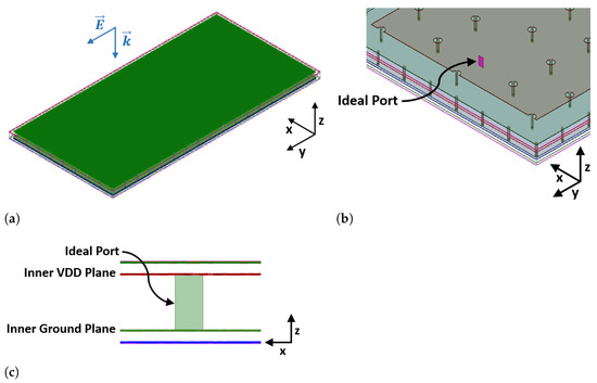
Figure 3.
Four-layer ideal PCB: (a) 3D model with incident wave normal to the top of the board ( direction) and -field polarized in the y direction, (b) 3D model port location, and (c) 2D model port location between inner planes.

Figure 4.
Four-layer PCB stackup including dielectric substrate, copper layers, and solder mask.
The plane wave angle of incidence and polarization was selected by first performing an emissions simulation for the ideal stackup. Due to the principal of reciprocity, it is expected that peak coupling will occur for a plane wave that is oriented based on peak emissions. Thus, the internal port was excited and the far-field radiation pattern was observed. This simulation indicated that the vast majority of energy is radiated in the positive and negative z directions with the -field polarized along the y axis. As a result, the plane wave was oriented in the same way as illustrated in Figure 3.
While holding all other parameters constant, the via fencing density is swept and the voltage at the ideal port is measured. Figure 5 shows the via fencing variations, and Figure 6 shows the results for these simulations.
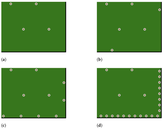
Figure 5.
Variations in via fencing density around the perimeter of the PCB: (a) no via fence, (b) 400 mil via spacing, (c) 100 mil via spacing, and (d) 20 mil via spacing. Images show the corner of each PCB design for easy comparison. Note that in all cases, via stitching is present internal to the board to tie all ground layers together.
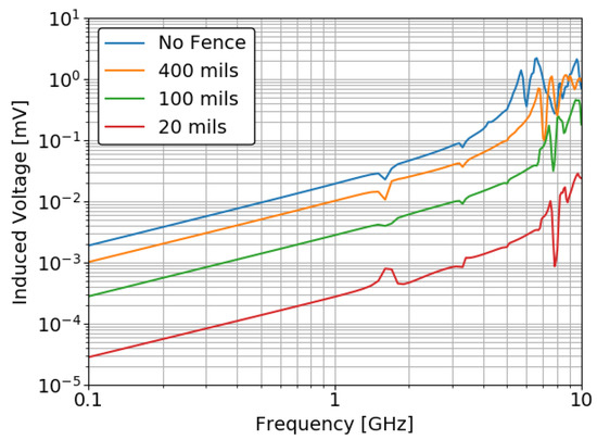
Figure 6.
Induced voltage on the power plane of a four-layer ideal PCB with varying via fencing density.
As shown in the plot, there is a clear trend in decreasing voltage as the via density increases, which is consistent with reduced emissions due to via fencing as presented in other literature. In fact, spacing the vias 20 mils apart results in a 35 to 45 dB reduction in induced voltage over most of the frequency range as compared to the design without via fencing. This is a substantial improvement, but again, care should be taken to avoid extending this observation to other dissimilar cases. Additional angles of incidence and polarizations for the ideal case show similar trends but are omitted here for the sake of brevity. Unfortunately, due to the ideal nature of this design, these results cannot be experimentally verified, but given the consistency with other simulations and experimental tests involving emissions, we can consider these data to be representative for an ideal PCB.
4.2. Radiated Susceptibility of Practical Multilayer PCB
In the practical PCB, component footprints and traces were introduced on the top layer. As illustrated in Figure 7, separate simulations are performed for three different angles of incidence described below:
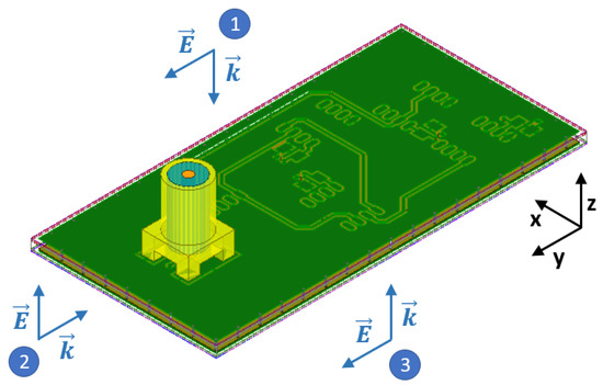
Figure 7.
Four-layer practical PCB with two separate incident wave scenarios. The practical design includes component footprints and traces on the top layer as well as a surface mount sub-miniature version A (SMA) connector model for experimental measurements.
- Case ①: wave propagates in the negative z direction () with the -field polarized along the y axis;
- Case ②: wave propagates in the negative y direction () with the -field polarized along the z axis;
- Case ③: wave propagates in the positive z direction () with the -field polarized along the y axis.
Each of these cases was selected by performing an emissions simulation and analyzing the far-field radiation pattern. By observing how the PCB radiates, we can also understand which angles and polarizations lead to maximum coupling. For this PCB, Case ① represents the orientation for maximum emissions, followed by Case ③ and Case ②.
Naturally, for the practical PCB designs, component footprints and traces create openings in the top ground plane where electromagnetic energy may enter. An SMA is also introduced with the center pin connected directly to the power plane through a short trace and via. Note that a surface mount SMA is used here as opposed to a through-hole connector in order to emulate an actual component with a power pin. The SMA is also included in the simulation to mimic experimental testing as much as is reasonably possible. Here again, the via fencing density is swept and the voltage at the SMA port is measured. The following sections present simulated data and experimental data along with associated discussions.
4.2.1. Practical PCB Simulation Results
The practical PCB designs were simulated using the same procedure and settings as the ideal designs. Figure 8 shows the simulated results for each angle of incidence and via fencing density. When reviewing the plots in Figure 8, we can make multiple observations, recognizing that the results are noticeably different from the ideal case. First, we see that in the practical design, the resonant modes are much more apparent, particularly at low frequencies. The induced voltage is also much higher in magnitude over most of the frequency range, suggesting that much more energy is reaching the power plane. In fact, if the peak voltage in Figure 8a (approximately 3 ) is scaled by a typical high intensity field (10 /), an induced voltage of 30 would be experienced by the circuit.

Figure 8.
Induced voltage on the power plane of a four-layer practical PCB with varying via fencing density: (a) plane wave propagating in the negative z direction (Case ①), (b) plane wave propagating in the negative y direction (Case ②), and (c) plane wave propagating in the positive z direction (Case ③). The shaded regions indicate where via fencing reduces induced voltage.
Additionally, and most notably, there is very little difference between each of the variations in via fencing density. At frequencies where the curves do deviate, via fencing mostly leads to reduced coupling, but sometimes actually leads to increased coupling. In areas where via fencing does reduce coupling, we see that via fencing can yield a 5 dB to 20 dB reduction in induced voltage (see shaded regions in Figure 8). This is obviously not nearly as good as the ideal case, and certainly does not span the entire frequency range, but it does represent an improvement that may be the difference between permanent damage and temporary malfunction.
Another significant observation is that we see very little notable difference for each angle of incidence and polarization. As expected, amplitude does vary to some degree because certain angles and polarizations can more efficiently excite resonant modes. However, the differences between each via fencing density are fairly consistent for all cases. This also held true for other angles of incidence and polarizations beyond the three cases presented here.
In light of these observations, it is clear that for the practical case presented here, the dominant coupling mechanism is electromagnetic energy that reaches the power plane through the openings in the top layer. In fact, nearly identical results are obtained when covering all PCB edges with perfect electric conductor (PEC) sheets, suggesting that very little energy is transferred through edge coupling. This is notable because results from previous works on emissions and via fencing certainly imply that via fencing might significantly reduce coupling—similar to the ideal scenario presented in the previous section. However, it is clear that in practical scenarios, that may not necessarily be the case.
Further confirmation of this conclusion was established through the use of transient simulations of the practical designs. By animating the fields in these transient simulations, it is apparent that energy does indeed reach the power plane through the narrow openings in the top layer. Energy certainly does leak through the edges of the PCB as well, but the behavior is clearly dominated by the energy entering through the top layer. This behavior is also observed even for fields incident on the edge of the board (Figure 8b) and the bottom of the board (Figure 8c).
To demonstrate the transient behavior described here, the trace layout of the practical PCB design was adjusted to yield three separate layouts, resulting in unique openings in the top layer. After performing the transient simulation, the surface current density was plotted on the power plane. The results for these simulations are shown in Figure 9 and demonstrate a behavior that is consistent with the previous simulation results. High surface current density is visible near the traces and pads, which is precisely where the top layer openings exist.
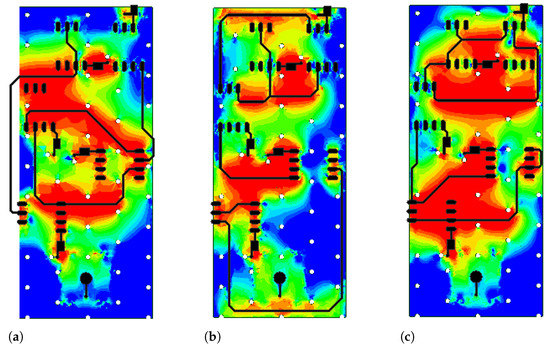
Figure 9.
Power plane surface current density for varying trace routing layouts: (a) Layout 1, (b) Layout 2, and (c) Layout 3. Pads and traces are colored black to indicate where openings in the top layer exist. The plots show that surface currents are first excited where openings exist, indicating that electromagnetic energy reaches the power plane through these openings.
4.2.2. Practical PCB Experimental Results
Although HFSS does enable unique field visualizations, it is still beneficial to perform model validation when possible. Furthermore, experimental data not only validate the model but also incorporate certain aspects that are difficult to model accurately or result in unacceptable simulation time. For model validation of the practical design, four identical PCBs were fabricated with varying via fencing density. The PCBs were fabricated on an FR4 substrate with a nominal permittivity of 4.27. Figure 10 shows images of each fabricated PCB with varying via fencing density. Experimental verification was performed using the procedure described in Section 3, and Figure 11 shows the comparison of simulated data vs. experimental data for a wave propagating in the negative z direction (Case ①). Additionally, Figure 12 shows the same data but separates the simulation curves from the experimental curves for an alternative comparison. As such, Figure 11 provides insight into model validation, while Figure 12 provides clarity on via fencing performance.
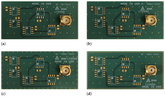
Figure 10.
Variations in via fencing density around the perimeter of the fabricated PCBs: (a) no via fence, (b) 400 mil via spacing, (c) 100 mil via spacing, and (d) 20 mil via spacing. Note that in all cases, via stitching is present internal to the board to tie all ground layers together.

Figure 11.
Comparison of simulated vs. experimentally measured induced voltage for each via fencing variation: (a) no via fence, (b) 400 mil via spacing, (c) 100 mil via spacing, and (d) 20 mil via spacing. The experimental data validate the modeling results and give further proof that the dominant coupling mechanism is not at the PCB edges.

Figure 12.
Comparison of simulated vs. experimentally measured induced voltage for a plane wave propagating in the negative z direction (Case ①): (a) simulation and (b) experimental. The experimental data deviate slightly from the simulation data but similarly demonstrate that via fencing density does not dramatically affect coupling.
As demonstrated in Figure 11, the experimental measurements match the simulated data quite well. For each via fencing variation, we see a similar magnitude of induced voltage across the frequency range with noticeable resonant peaks at similar locations. As expected, there is some deviation, which can be attributed to a few potential factors. The model is based on nominal dimensions, which are certainly going to vary during fabrication. In fact, measurements of the fabricated PCBs indicate that the boards are slightly thicker than nominal thickness. The inner layer spacing is also likely to be slightly different as well. Additionally, a constant permittivity value is used in the model, but in reality, the permittivity will actually vary with frequency, particularly with an FR4 substrate. The cable used for the experimental measurements is also not included in the model, and it will certainly affect the fields near the PCB. Nevertheless, the results match well, even with these differences. These data serve to validate both the model and the experimental procedure, which is a non-trivial task when dealing with radiated testing.
With respect to experimental data in Figure 12b, we actually see even less variation in induced voltage between via fencing densities. As with the simulation results, sometimes coupling decreases with via fencing, while other times it increases. However, other angles of incidence do show greater deviation between the curves with via fencing, generally reducing induced voltage by a small margin.
5. Discussion
To our knowledge, the work presented here is not only unique but also critical to further understanding the primary board-level coupling mechanisms and associated mitigation techniques. Contrary to potential conclusions drawn from previous work on via fencing, these data suggest that via fencing does not necessarily play a substantial role in coupling for practical PCBs. However, the data do indicate that via fencing offers slight improvements at certain frequencies. Given that via fencing has little to no effect on fabrication cost, it is therefore advantageous to incorporate them into practical designs. Edge plating, on the other hand, can substantially increase cost, but does not seem to offer additional protection beyond traditional via fencing.
An important note to make here is on the applicability of these data to other scenarios. As emphasized throughout this work, we should be hesitant to apply these conclusions to other dissimilar cases. The behavior seen here can likely be extended to other stackups with a power plane adjacent to an outer signal layer, which allows electromagnetic energy to directly excite surface currents on the power plane. Other stackups may not exhibit the same behavior.
For example, a six-layer PCB would enable placing a shielding layer between the top signal layer and the inner power plane. This topology may actually shift the dominant coupling mechanism to edge coupling, which would certainly be mitigated with high density via fencing. Future work will involve investigation of this scenario as well as other stackups. Additionally, future work will expand beyond via fencing and include other board-level parameters, including power plane pullback, layer separation and board thickness, substrate permittivity, and substrate losses. It is expected that further information on board-level radiated susceptibility will enable the development of PCB design guidelines that are effective for systems expected to experience HIRF environments.
Author Contributions
Conceptualization, R.P.T. and J.-W.C.; methodology, R.P.T., W.M., E.R. and W.B.; software, W.M. and E.R.; validation, W.M. and E.R.; formal analysis, R.P.T. and W.M.; investigation, R.P.T., W.M., E.R., W.B. and J.-W.C.; data curation, R.P.T. and E.R.; writing—original draft preparation, R.P.T.; writing—review and editing, R.P.T., W.M., E.R., W.B. and J.-W.C. All authors have read and agreed to the published version of the manuscript.
Funding
This research received no external funding.
Data Availability Statement
The data presented in this study are available on request from the corresponding author.
Conflicts of Interest
The authors declare no conflict of interest.
References
- High-Intensity Radiated Fields (HIRF) Protection for Aircraft Electrical and Electronic Systems; Proposed Rule, 71 F.R. 5553; Federal Register: Washington, DC, USA, 2006.
- High-Intensity Radiated Fields (HIRF) Protection for Aircraft Electrical and Electronic Systems; Final Rule, 72 F.R. 44015; Federal Register: Washington, DC, USA, 2007.
- High-intensity Radiated Fields (HIRF) Protection; 14 C.F.R. § 23.1308; Federal Register: Washington, DC, USA, 2007.
- High-intensity Radiated Fields (HIRF) Protection; 14 C.F.R. § 25.1317; Federal Register: Washington, DC, USA, 2007.
- High-intensity Radiated Fields (HIRF) Protection; 14 C.F.R. § 27.1317; Federal Register: Washington, DC, USA, 2007.
- High-intensity Radiated Fields (HIRF) Protection; 14 C.F.R. § 29.1317; Federal Register: Washington, DC, USA, 2007.
- The Certification of Aircraft Electrical and Electronic Systems for Operation in the High-intensity Radiated Fields (HIRF) Environment. In Fed. Aviat. Adm. Advisory Circular, AC No: 20-158A; Federal Aviation Administration: Washington, DC, USA, 2014.
- Heather, F.W. High intensity radiated field external environments for civil aircraft. In Proceedings of the IEEE International Symposium on Electromagnetic Compatability, Seattle, WA, USA, 2–6 August 1999; pp. 963–968. [Google Scholar] [CrossRef]
- Bäckström, M.G.; Lövstrand, K.G. Susceptibility of electronic systems to high-power microwaves: Summary of test experience. IEEE Trans. Electromagn. Compat. 2004, 46, 396–403. [Google Scholar] [CrossRef]
- Larsson, A.; Johansson, B.; Nyholm, S.E. Radiated electric field strength from high-power microwave systems. IEEE Trans. Electromagn. Compat. 2008, 50, 758–761. [Google Scholar] [CrossRef]
- Steinar, B. The Physics of HPM Sources; FFI Report; Norwegian Defense Research Establishment: Kjeller, Norway, 2008. [Google Scholar]
- Shurenkov, V.; Pershenkov, V. Electromagnetic pulse effects and damage mechanism on the semiconductor electronics. Electron. Energ. 2016, 29, 621–629. [Google Scholar] [CrossRef]
- Goransson, G. HPM effects on electronic components and the importance of this knowledge in evaluation of system susceptibility. In Proceedings of the IEEE International Symposium on Electromagnetic Compatability, Seattle, WA, USA, 2–6 August 1999; pp. 543–548. [Google Scholar] [CrossRef]
- Radasky, W.A.; Bäckström, M. Brief historical review and bibliography for Intentional Electromagnetic Interference (IEMI). In Proceedings of the 2014 XXXIth URSI General Assembly and Scientific Symposium, Beijing, China, 16–23 August 2014; pp. 1–4. [Google Scholar] [CrossRef]
- Du, J.K.; Hwang, S.M.; Ahn, J.W.; Yook, J.G. Analysis of coupling effects to PCBs inside waveguide using the modified BLT equation and full-wave analysis. IEEE Trans. Microw. Theory Tech. 2013, 61, 3514–3523. [Google Scholar] [CrossRef]
- Bernardi, P.; Cicchetti, R. Response of a Planar Microstrip Line Excited by an External Electromagnetic Field. IEEE Trans. Electromagn. Compat. 1990, 32, 98–105. [Google Scholar] [CrossRef]
- Bernardi, P.; Cicchetti, R.; Pirone, C. Transient response of a microstrip line circuit excited by an external electromagnetic source. IEEE Trans. Electromagn. Compat. 1992, 34, 100–108. [Google Scholar] [CrossRef]
- Leone, M.; Singer, H.L. On the coupling of an external electromagnetic field to a printed circuit board trace. IEEE Trans. Electromagn. Compat. 1999, 41, 418–424. [Google Scholar] [CrossRef]
- Leone, M. Radiated susceptibility on the printed-circuit-board level: Simulation and measurement. IEEE Trans. Electromagn. Compat. 2005, 47, 471–478. [Google Scholar] [CrossRef]
- Veropoulos, G.P.; Papakanellos, P.J.; Vlachos, C. A Probabilistic Approach for the Susceptibility Assessment of a Straight PCB Trace Excited by Random Plane-Wave Fields. IEEE Trans. Electromagn. Compat. 2018, 60, 258–265. [Google Scholar] [CrossRef]
- Silfverskiöld, S.; Bäckström, M.; Lorén, J. Microwave field-to-wire coupling measurements in anechoic and reverberation chambers. IEEE Trans. Electromagn. Compat. 2002, 44, 222–232. [Google Scholar] [CrossRef]
- Kim, S.; Lee, J.; Choi, J.S.; Yook, J.G. Analysis of Electromagnetic Pulse Coupling into Electronic Device Considering Wire and PCB Resonance. In Proceedings of the 2018 International Symposium on Antennas and Propagation, Busan, Korea, 23–26 October 2018; pp. 521–522. [Google Scholar]
- Kim, S.; Noh, Y.H.; Lee, J.; Lee, J.; Choi, J.S.; Yook, J.G. Electromagnetic Signature of a Quadcopter Drone and Its Relationship with Coupling Mechanisms. IEEE Access 2019, 7, 174764–174773. [Google Scholar] [CrossRef]
- Paul, C.R. Introduction to Electromagnetic Compatibility; Wiley: Hoboken, NJ, USA, 2006. [Google Scholar]
- Nana, R.K.; Korte, S.; Dickmann, S.; Garbe, H.; Sabath, F. Estimation of the threat of IEMI to complex electronic systems. Adv. Radio Sci. 2009, 7, 249–253. [Google Scholar] [CrossRef]
- Nana, R.K.; Dickmann, S.; Schetelig, B.; Keghie, J.; Sabath, F. Estimation of the threat of IEMI to marine equipment and EM hardening solutions. In Proceedings of the International Conference on Electromagnetics in Advanced Applications, Turin, Italy, 14–18 September 2009; pp. 51–54. [Google Scholar] [CrossRef]
- Nana, R.K.; Dickmann, S.; Sabath, F. Electromagnetic field vulnerability of complex systems-an application of EM topology. Adv. Radio Sci. 2008, 6, 273–277. [Google Scholar] [CrossRef]
- Abadpour, S.; Dehkhoda, P.; Karami, H.R.; Moini, R. Aperture size effect on the susceptibility of a PCB inside an enclosure. In Proceedings of the International Conference on Electromagnetics in Advanced Applications, Turin, Italy, 12–16 September 2011; pp. 741–744. [Google Scholar] [CrossRef]
- Du, J.K.; Ahn, J.W.; Hwang, S.M.; Yook, J.G. Analysis of coupling effects in waveguides using the BLT Equation and Numerical Methods. In Proceedings of the IEEE/MTT-S International Microwave Symposium Digest, Montreal, QC, Canada, 17–22 June 2012; pp. 1–3. [Google Scholar] [CrossRef]
- Du, J.K.; Kim, Y.; Yook, J.G.; Lee, J.; Choi, J.S. Coupling effects of incident electromagnetic waves to multilayered PCBs in metallic enclosures. In Proceedings of the International Workshop on Antenna Technology, Seoul, Korea, 4–6 March 2015; pp. 359–361. [Google Scholar] [CrossRef]
- Kreitlow, M.; Sabath, F.; Garbe, H. Analysis of IEMI effects on a computer network in a realistic environment. In Proceedings of the IEEE International Symposium on Electromagnetic Compatibility (EMC 2015), Dresden, Germany, 16–22 August 2015; pp. 1063–1067. [Google Scholar] [CrossRef]
- Chen, H.C.; Bai, Y.W. Improvement of high current density PCB design on a high end server system. In Proceedings of the 2013 IEEE International Symposium on Industrial Electronics, Taipei, Taiwan, 28–31 May 2013. [Google Scholar] [CrossRef]
- Suntives, A.; Khajooeizadeh, A.; Abhari, R. Using via fences for crosstalk reduction in PCB circuits. In Proceedings of the 2006 IEEE International Symposium on Electromagnetic Compatibility, Portland, OR, USA, 14–18 August 2006; pp. 34–37. [Google Scholar] [CrossRef]
- Zhi, L.; Wang, Q.; Shi, C. Application of guard traces with vias in the RF PCB layout. In Proceedings of the IEEE International Symposium on Electromagnetic Compatibility, Beijing, China, 21–24 May 2002; pp. 771–774. [Google Scholar] [CrossRef]
- Anupama, V.; Salil, P. Analysis of different techniques for reduction of SI and emission from PCB trace. In Proceedings of the 2013 International Conference on Emerging Trends in VLSI, Embedded System, Nano Electronics and Telecommunication System (ICEVENT), Tiruvannamalai, India, 7–9 January 2013. [Google Scholar] [CrossRef]
- Gisin, F.; Pantic-Tanner, Z. Minimizing EMI caused by radially propagating waves inside high speed digital logic PCBs. In Proceedings of the 2013 International Conference on Emerging Trends in VLSI, Embedded System, Nano Electronics and Telecommunication System (ICEVENT), Tiruvannamalai, India, 7–9 January 2013; pp. 624–631. [Google Scholar] [CrossRef]
- Gisin, F.; Pantic-Tanner, Z. Radiation from printed circuit board edge structures. In Proceedings of the 2001 IEEE EMC International Symposium. Symposium Record. International Symposium on Electromagnetic Compatibility, Montreal, QC, Canada, 13–17 August 2001; pp. 881–883. [Google Scholar] [CrossRef]
- Xu, H.Y.; Zhang, M.S.; Tan, H.Z. Modeling and comparison of different edge radiation suppression methods in printed circuit boards. In Proceedings of the 15th International Conference on Electronic Packaging Technology, Chengdu, China, 12–15 August 2014; pp. 551–554. [Google Scholar] [CrossRef]
- Montrose, M.I. Voltage and return plane bounce affecting digital components using different printed circuit board edge termination methodologies. IEEE Trans. Electromagn. Compat. 2011, 53, 802–805. [Google Scholar] [CrossRef]
- Montrose, M.I.; Liu, E.X. Power and ground bounce effects on component performance based on printed circuit board edge termination methodologies. In Proceedings of the 2007 IEEE International Symposium on Electromagnetic Compatibility, Honolulu, HI, USA, 9–13 July 2007. [Google Scholar] [CrossRef]
- Montrose, M.I.; Liu, E.X. Radiated emission analysis from printed circuit board edges using multiple stimulus sources. In Proceedings of the 2006 17th International Zurich Symposium on Electromagnetic Compatibility, Singapore, 27 February–3 March 2006; pp. 574–577. [Google Scholar] [CrossRef]
- Montrose, M.I.; Li, E.P.; Jin, H.F.; Yuan, W.L. Analysis on the effectiveness of the 20-H rule for printed-circuit-board layout to reduce edge-radiated coupling. IEEE Trans. Electromagn. Compat. 2005, 47, 227–233. [Google Scholar] [CrossRef]
- Montrose, M.I.; Enxiao, L.; Li, E.P. Analysis on the effectiveness of printed circuit board edge termination using discrete components instead of implementing the 20-H Rule. In Proceedings of the 2004 International Symposium on Electromagnetic Compatibility (IEEE Cat. No.04CH37559), Silicon Valley, CA, USA, 9–13 August 2004; pp. 45–50. [Google Scholar] [CrossRef]
- Montrose, M.I.; Hong-Fang, J.; Li, E.P. Analysis on the effectiveness of high speed printed circuit board edge radiated emissions based on stimulus source location. In Proceedings of the 2004 International Symposium on Electromagnetic Compatibility (IEEE Cat. No.04CH37559), Silicon Valley, CA, USA, 9–13 August 2004; pp. 51–56. [Google Scholar] [CrossRef]
- Li, E.P.; Yuan, W.L.; Yi, J.; Li, L.W.; Montrose, M.I. Analysis on the effectiveness of the 20-H rule using numerical simulation technique. In Proceedings of the 2002 IEEE International Symposium on Electromagnetic Compatibility, Minneapolis, MN, USA, 19–23 August 2002; pp. 328–333. [Google Scholar] [CrossRef]
- Chiappe, J. A comparison of relative shielding provided by stitching vias and edge plating. In Proceedings of the 2015 IEEE Symposium on Electromagnetic Compatibility and Signal Integrity, Santa Clara, CA, USA, 15–21 March 2015; pp. 101–106. [Google Scholar] [CrossRef]
- Ye, X.; Hockanson, D.M.; Li, M.; Ren, Y.; Cui, W.; Drewniak, J.L.; DuBroff, R.E. EMI mitigation with multilayer power-bus stacks and via stitching of reference planes. IEEE Trans. Electromagn. Compat. 2001, 43, 538–548. [Google Scholar] [CrossRef]
- Cao, Y.S.; Wang, Y.; Wu, S.; Yang, Z.; Fan, J. PCB Edge Shielding Effectiveness Evaluation and Design Guidelines. In Proceedings of the 2018 IEEE Symposium on Electromagnetic Compatibility, Signal Integrity and Power Integrity (EMC, SI & PI), Long Beach, CA, USA, 30 July–3 August 2018. [Google Scholar] [CrossRef]
- Lindseth, W. Effectiveness of PCB perimeter Via fencing: Radially propagating EMC emissions reduction technique. In Proceedings of the 2016 IEEE International Symposium on Electromagnetic Compatibility (EMC), Ottawa, ON, Canada, 25–29 July 2016; pp. 627–632. [Google Scholar] [CrossRef]
- Wu, X.; Kermani, M.H.; Ramahi, O.M. Mitigating multi-layer PCB power bus radiation through novel mesh fencing techniques. In Proceedings of the Electrical Performance of Electrical Packaging (IEEE Cat. No. 03TH8710), Princeton, NJ, USA, 27–29 October 2003; pp. 207–210. [Google Scholar] [CrossRef]
- Wu, X. Resistive fencing technique for multi-layer PCB power bus radiation mitigation. In Proceedings of the 2004 3rd International Conference on Computational Electromagnetics and Its Applications, Beijing, China, 1–4 November 2004; pp. 276–279. [Google Scholar] [CrossRef]
- Shahparnia, S.; Ramahi, O.M. Electromagnetic interference (EMI) reduction from printed circuit boards (PCB) using electromagnetic bandgap structures. IEEE Trans. Electromagn. Compat. 2004, 46, 580–587. [Google Scholar] [CrossRef]
- Wang, L.; Schuster, C. Investigation of Radiated EMI from Printed Circuit Board Edges up to 100 GHz by Using an Effective Two-Dimensional Approach. In Proceedings of the 2018 International Symposium on Electromagnetic Compatibility (EMC EUROPE), Amsterdam, The Netherlands, 27–30 August 2018; pp. 473–476. [Google Scholar] [CrossRef]
- Chen, R.L.; Chen, J.; Hubing, T.H.; Shi, W. Analytical model for the rectangular power-ground structure including radiation loss. IEEE Trans. Electromagn. Compat. 2005, 47, 10–16. [Google Scholar] [CrossRef]
- Lo, Y.T.; Solomon, D.; Richards, W.F. Theory and Experiment on Microstrip Antennas. IEEE Trans. Antennas Propag. 1979, 27, 137–145. [Google Scholar] [CrossRef]
- Xu, M.; Hubing, T.H. Estimating the power bus impedance of printed circuit boards with embedded capacitance. IEEE Trans. Adv. Packag. 2002, 25, 424–432. [Google Scholar] [CrossRef]


Publisher’s Note: MDPI stays neutral with regard to jurisdictional claims in published maps and institutional affiliations. |
© 2021 by the authors. Licensee MDPI, Basel, Switzerland. This article is an open access article distributed under the terms and conditions of the Creative Commons Attribution (CC BY) license (http://creativecommons.org/licenses/by/4.0/).