Abstract
This work proposes a novel linearized low noise amplifier (LNA) for X-band applications with flat power gain, low noise performance and enhanced linearity. In this study, a triple-cascode topology with dual-resonant network is utilized and a modified post-distortion network is introduced to improve the linearity. The LNA utilizes a subthreshold auxiliary NMOS transistor to reduce the nonlinearity with low power consumption. In addition, a methodology is proposed to predict the characteristic of the linearity performance of the proposed LNA with modified post-distortion network. With a small increase of 1 mW in power consumption due to the inclusion of the post-distortion network, the input intercept point IIP3 is improved and lies in the range of −3 to +8 dBm over the frequency range from 8 to 12 GHz. Implemented in Global Foundries 130 nm CMOS process, the LNA achieves a peak gain of 18 dB, and a 1.3 dB minimum NF over 8 to 12 GHz. The proposed LNA requires an area of 1.2 and a power of 18 mW.
1. Introduction
Growing research space applications and radar systems has aroused interest in broadband LNAs. A broadband LNA needs to provide good input matching, high linearity, flat power gain, and low noise figure (NF) over a multi-GHz bandwidth (BW) while consuming low power and die area.
To achieve broadband input matching, band-pass filtering (BPF) network, feedback network, common-gate (CG) stage, and inductive source degeneration techniques have been proposed [1,2,3,4]. However, the BPF network requires a large amount of inductance and capacitance leading to an increased area and degraded noise performance. Feedback network increases the noise figure. Although common-gate stage makes the impedance for a wider frequency band, its noise figure is greater than the common source stage. On the other hand, a conventional inductive source degradation structure has difficulty achieving wideband input matching.
A non-negligible challenge to broadband LNAs is the stringent linearity requirement over a wide frequency range because of the large numbers of in-band interferences in wideband systems. Cross modulation and inter modulation are caused by blockers and transmitter leakage [5] in a reconfigurable receiver. Higher linearity is also required to suppress interference and maintain a high sensitivity [6]. Therefore, in the CMOS process, many linearization techniques have been proposed to meet the demand of broadband linearization.
Optimizing overdrive voltage [5,7] leads to a linearity boost region for a fairly narrow range of input amplitude. Using second-order nonlinear parameters to suppress third-order nonlinearity, the feedback technology can improve linearity in a wide frequency band, while the loop gain is limited [8]. A derivative superposition (DS) method [9] uses an additional transistor’s nonlinearity to cancel that of the main device. It utilizes MOS transistors working in a triode or weak inversion region. However, the common problem existing in all the reported DS methods is its difficulty with achieving good input matching and optimized noise performance. Post-distortion usually achieves stable distortion rejection and high linearity with an auxiliary saturated transistor, while the auxiliary transistors consume extra power to operate in saturation mode [10,11]. Several post-distortion (PD) networks have been proposed to enhance the linearity of LNA [10,12,13]. An auxiliary PMOS transistor has been employed to absorb the nonlinear current over a wide frequency range [10]. A folded PMOS intermodulation distortion (IMD) sinker has been proposed to absorb IMD3 current generated by the main transistor [12]. A diode connected transistor has been utilized to linearize the main transistor [13]. A conventional post-distortion technology method will degrade IIP3 performance due to the contribution of the second-order nonlinearity of [14]. However, few studies have been published to discuss how to improve linearity in a high frequency region.
In this paper, a triple-cascode LNA with a modified post-distortion network is introduced, which has a simple input matching network to expand bandwidth and enhanced linearity compared to prior reported LNAs with conventional post-distortion technique. The proposed post-distortion network is composed of transistor operating in a weak inversion region consuming low power. An auxiliary is augmented at the source node of to enhance linearity at high frequency region.
The paper is organized as follows: Section 2 details the design method of the proposed X-band linearized LNA including analysis for the input matching network, power gain, and novel post-distortion technology. Section 3 presents simulated performances of the proposed LNA. Finally, conclusions are given in Section 4.
2. Triple-Cascode LNA with a Modified Post-Distortion Network Analysis
2.1. Input Matching Analysis
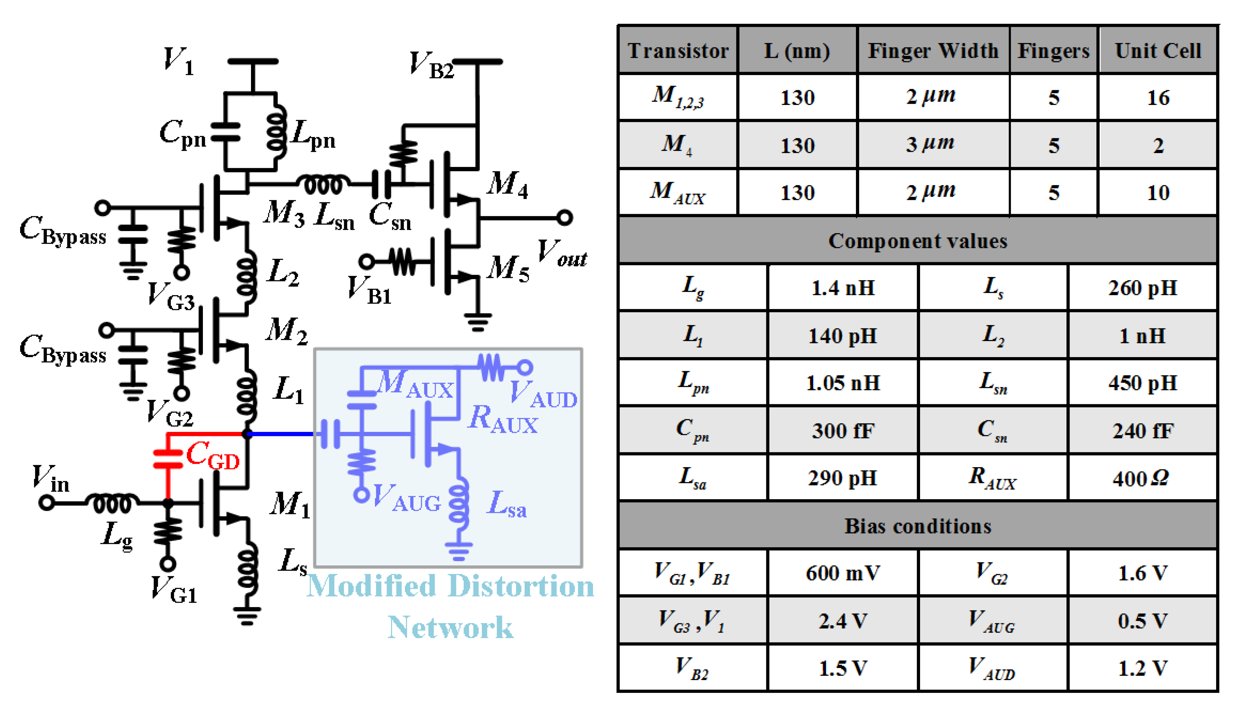
The proposed triple-cascode LNA with a modified post-distortion network is shown in Figure 1. The conventional inductive source degeneration common-source CS-LNA is accomplished by making its real part , where is source impedance. Inductance is connected in series with gate node of to adjust the imaginary part of input impedance. By taking parasitic capacitance into account or by augmenting an extra capacitance , the input matching bandwidth can be extended. The input impedance of the proposed triple-cascode LNA can be written as
where Z represents load impedance seen from the drain node of transistor of and can approximately be expressed as

Figure 1.
Schematic of the proposed triple-cascode LNA with the modified post-distortion network.
Based on input impedance analysis and network analysis, the calculation of −10 dB bandwidth for input matching can be derived from the following equations:
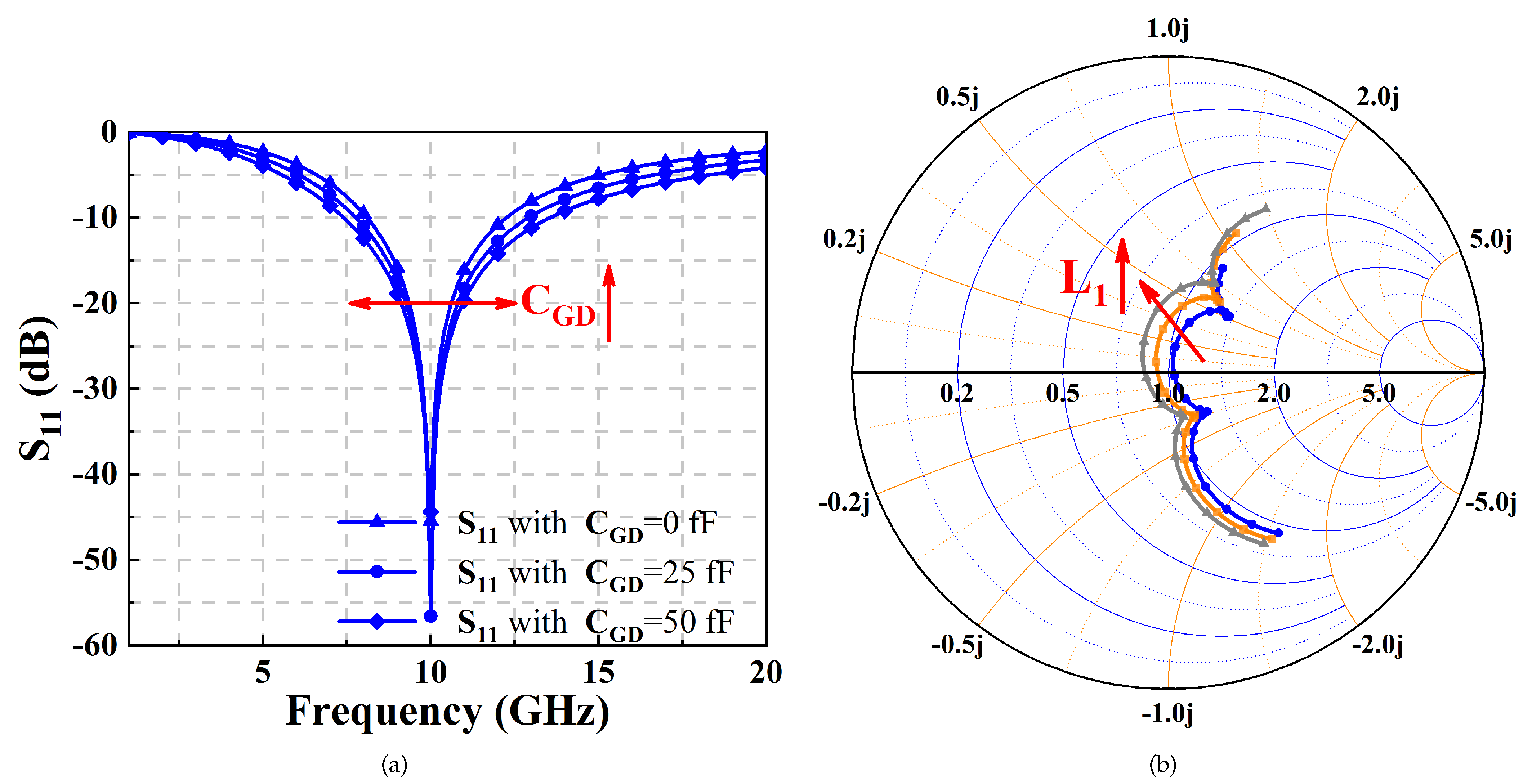
As shown in Equation (1), the parasitic capacitance combined with load impedance seen from the drain node of transistor can regulate the input impedance, which in turn can extend input matching bandwidth. The detailed calculus given in Equations (1)–(3) essentially provides a generalized method to calculate the input matching bandwidth with an arbitrary input matching network. Generally, the numerator, denominator in Equation (3b) can be calculated based on input impedance. The numerator and denominator in Equation (3b) are calculated in Appendix A. Numerator and Denominator for Bandwidth Calculation. To verify the generalized method, input matching bandwidth of the proposed LNA is calculated based on Equations (1)–(3). and need to be changed to fix the resonant frequency. The calculated , , input bandwidth with different are listed in Table 1. The calculated result shows identical simulated value as shown in Figure 2a. Figure 2 plots the of input matching network by increasing from 100 pH to 300 pH to verify the regulating effect with the existence of . Compared with other broadband matching technologies, although the method using has a complicated load calculation, it can effectively extend the input matching bandwidth compared with a conventional inductive source degeneration technique without compensation.

Table 1.
Calculated , , Bandwidth with Different .

Figure 2.
(a) Conceptual diagram of bandwidth extension with compensation of in dB format; (b) simulated with increasing from 100 pH to 300 pH in the Smith chart format.
2.2. Gain Analysis
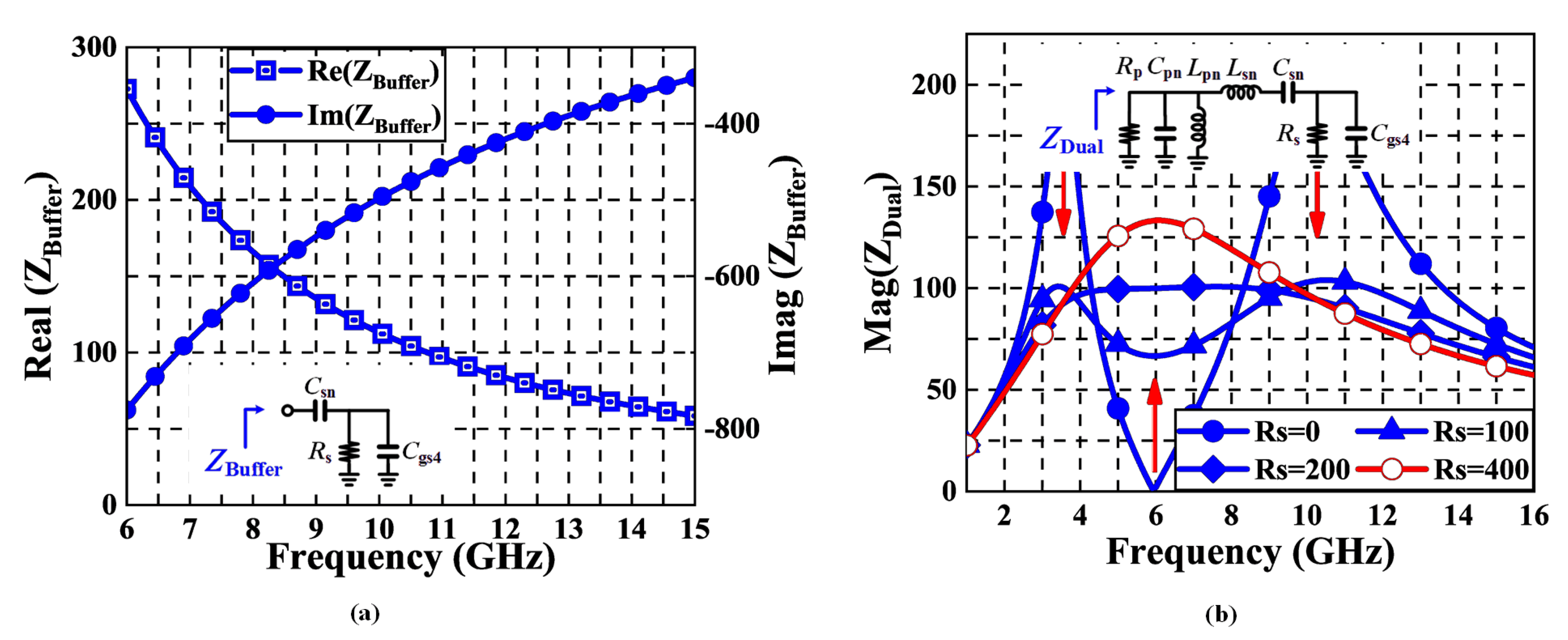
The proposed triple-cascode LNA incorporates a dual-resonant network. For in the output buffer, three parallel multifinger transistors with unit transistor size of W = 2 μm, L = 130 nm, and number of fingers N = 5 are used. The input impedance of the output buffer can be modeled as a parallel RC circuit as shown in Figure 3a. The capacitance and resistance can be extracted based on simulated input impedance. The gain analysis can be done by analyzing the characteristics of the dual-resonant network. According to an equivalent model of the dual-resonant network in Figure 3b, the impedance magnitude of the dual-resonant network can be written as
where
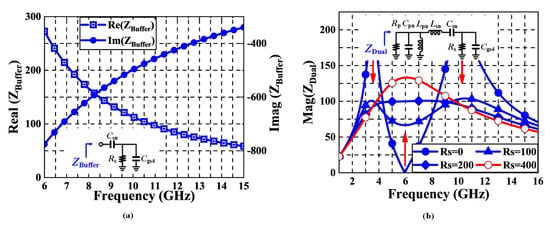
Figure 3.
Dual resonant network. (a) simulated real and imaginary part and equivalent circuit of the output buffer; (b) equivalent circuit of dual resonant network and conceptual flat gain mechanism.
To derive two peak resonant gain, we firstly neglect resistance in the series and parallel branch. Then, the two peak resonant frequency can be approximately calculated as
By utilizing parasitic capacitance and resistance seen from gate node of output buffer, the magnitude of the load impedance can be enhanced between two resonant frequency points, which results in flat gain. Therefore, the design of the load network is simplified by choosing proper inductance and designing output buffer stage, which results in double resonant effect and flat power gain.
2.3. Noise Analysis
The noise model for inductively degenerated triple-cascode LNA is shown in Figure 4, the noise factor (F) of CS-LNA can be defined as [15]
where is the Boltzmann constant, T is absolute temperature, , , are the conductance of the transistor , , when the voltage between the drain and source node equals to zero, respectively. , , represent the series metal loss of inductor , and gate resistor of , respectively. Parasitic resistance of the inductors can be noise sources to degrade NF performance. To investigate the effective parasitic parameters of the inductors, inductors used in the circuit have been simulated in Figure 5.
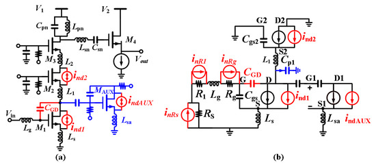
Figure 4.
(a) Noise model for the inductively degenerated triple-cascode LNA; (b) equivalent circuit model for the calculation of noise performance.

Figure 5.
(a) Simulated parasitic series resistance of inductors; (b) simulated quality factor Q of inductors; (c) simulated effective inductance of inductors.
Furthermore, parasitic capacitance of and at the source node degrades the noise performance as frequency increases. As shown in Equations (6) and (7), for simplicity, is neglected when calculate . According to Equation (7), ideally, the noise contribution can be cancelled [16] when
Hence, we introduce two inductors between , and to resonate parasitic capacitance, which results in enhanced noise performance. By utilizing simultaneous noise input matching technology, the triple-cascode LNA can achieve input matching and the minimum noise figure simultaneously. On the other hand, the noise performance can be degraded by gate resistance of transistor significantly. One can improve the noise performance by reducing the gate resistance. The gate resistance can be expressed as the following equation:
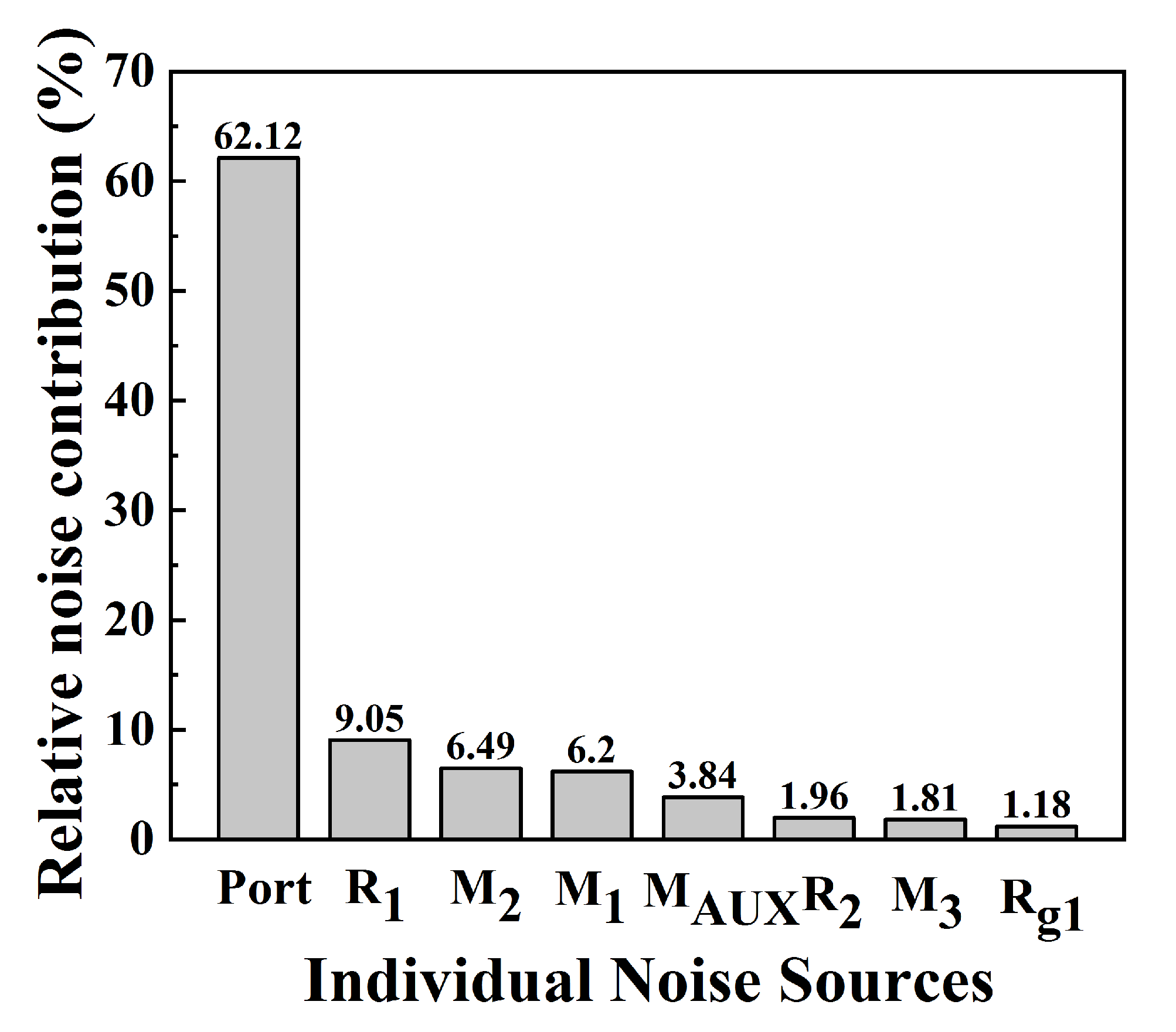
where is gate sheet resistance, W is total gate finger width, n is number of fingers, and L is the gate length. According to the above analysis, by optimizing the transistor layout, input matching network, and bias condition, the proposed triple-cascode LNA can achieve low noise performance and enhanced input matching bandwidth. Simulated noise contributions by individual components of proposed LNA are shown in Figure 6.
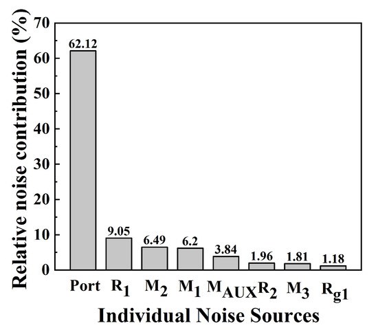
Figure 6.
Simulated noise contributions by individual components in proposed LNA.
2.4. Linearity Analysis
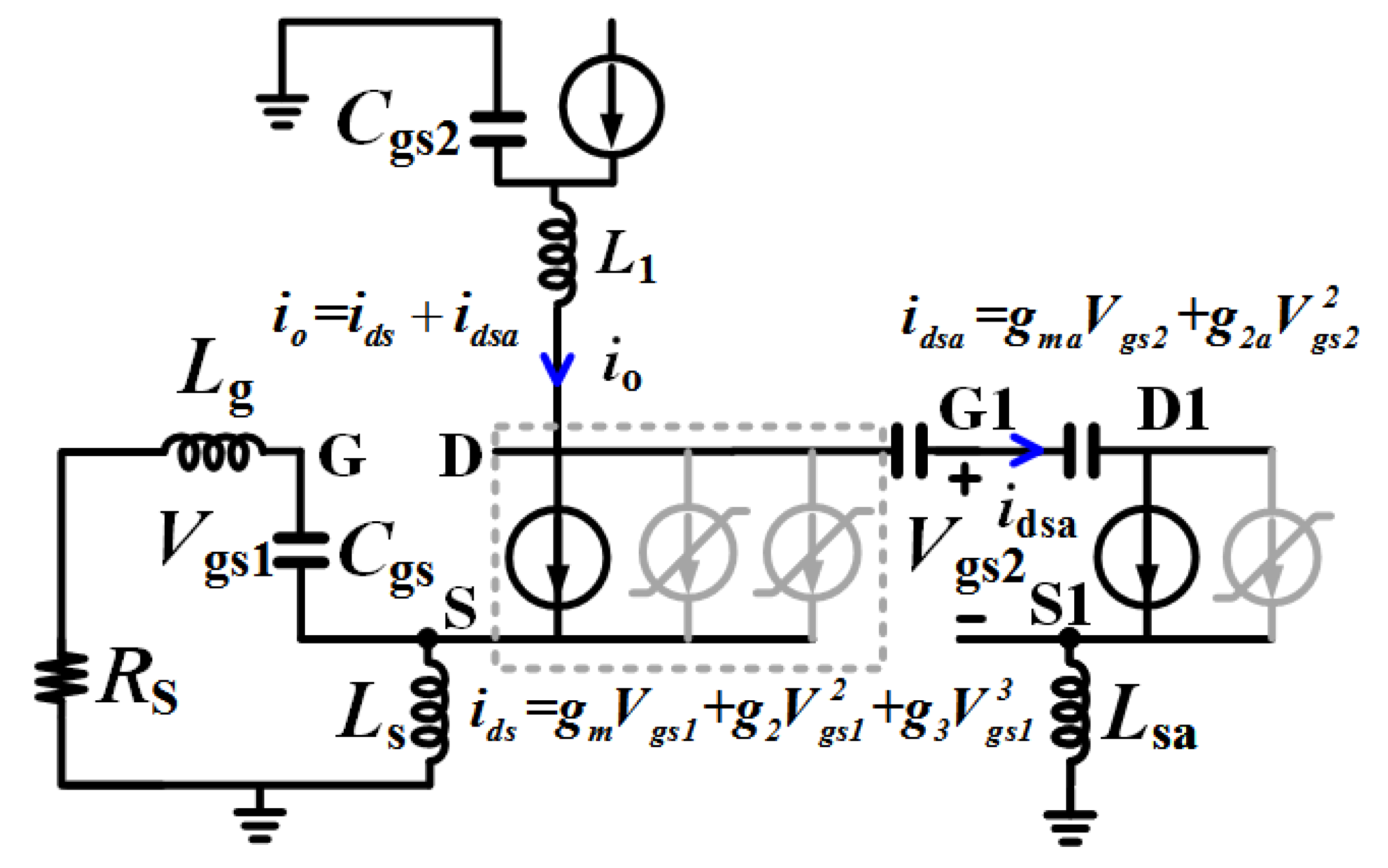
The linearization technique based on optimum gate biasing has been proposed to generate zero 3rd-order nonlinearity coefficient [7]. Derivatives of the drain-source dc current of transistor , with respect to (, ) have been illustrated in Figure 7 and Figure 8. However, the optimum gate biasing technique can only improve the IIP3 in a very narrow range, which is sensitive to process and temperature variations. The modified derivative superposition method has been proposed to eliminate the contribution of the second-order nonlinearity [14]. On the other hand, the modified derivative superposition technique complicates the input matching network to simultaneously achieve good input matching and low noise performance. We propose the triple-cascode configuration LNA combined with a post-distortion network to improve the linearity with a simple input matching network and low noise performance. Although the work in [17] looks similar to a triple-cascode configuration, it is actually a two stage amplifier with the CS and cascode stage in current reuse topology. The reported current-reuse LNA utilized the modified derivative superposition technique to improve the linearity [18]. Essentially, triple-cascode can provide enhancement of linearity [19]. Volterra series has been utilized to analyze linearity of the triple-cascode LNA [13,14,20,21]. The linearity of proposed triple-cascode LNA is dominantly determined by the CS stage. For simplicity, the CG stage is regarded as a linear current buffer as shown in Figure 9, which plays a non-dominated role in linearity analysis [13]. Furthermore, the linearity analysis at the drain node of transistor , according to the simulated result shown in Figure 10, approximately equals the linearity analysis at the drain node of transistor . To calculate linearity of the proposed LNA, the drain current of transistor and auxiliary transistor can be modeled up to the third-order and second-order as

Figure 7.
and derivatives versus of main transistor . (a) ; (b) ; (c) ; (d) .

Figure 8.
and derivatives versus of auxiliary transistor . (a) ; (b) ; (c) ; (d) .
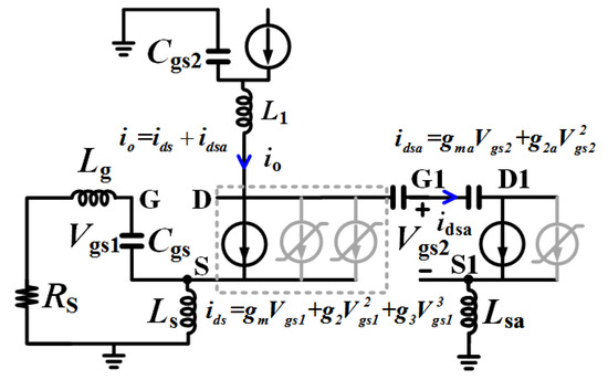
Figure 9.
Equivalent circuit model for calculation of linearity.
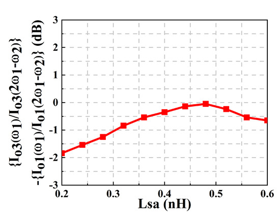
Figure 10.
Linearity analysis at the drain node transistor of and .
The voltage between gate and source node of transistor , and output current can be considered up to third-order with Volterra theory as the following equations:
By utilizing the above Volterra series kernels, the output current can be written as
The above Volterra series kernels are calculated in Appendix B. Volterra Expansion Analysis. The third-order intercept point IIP3 could be further expressed as [14]
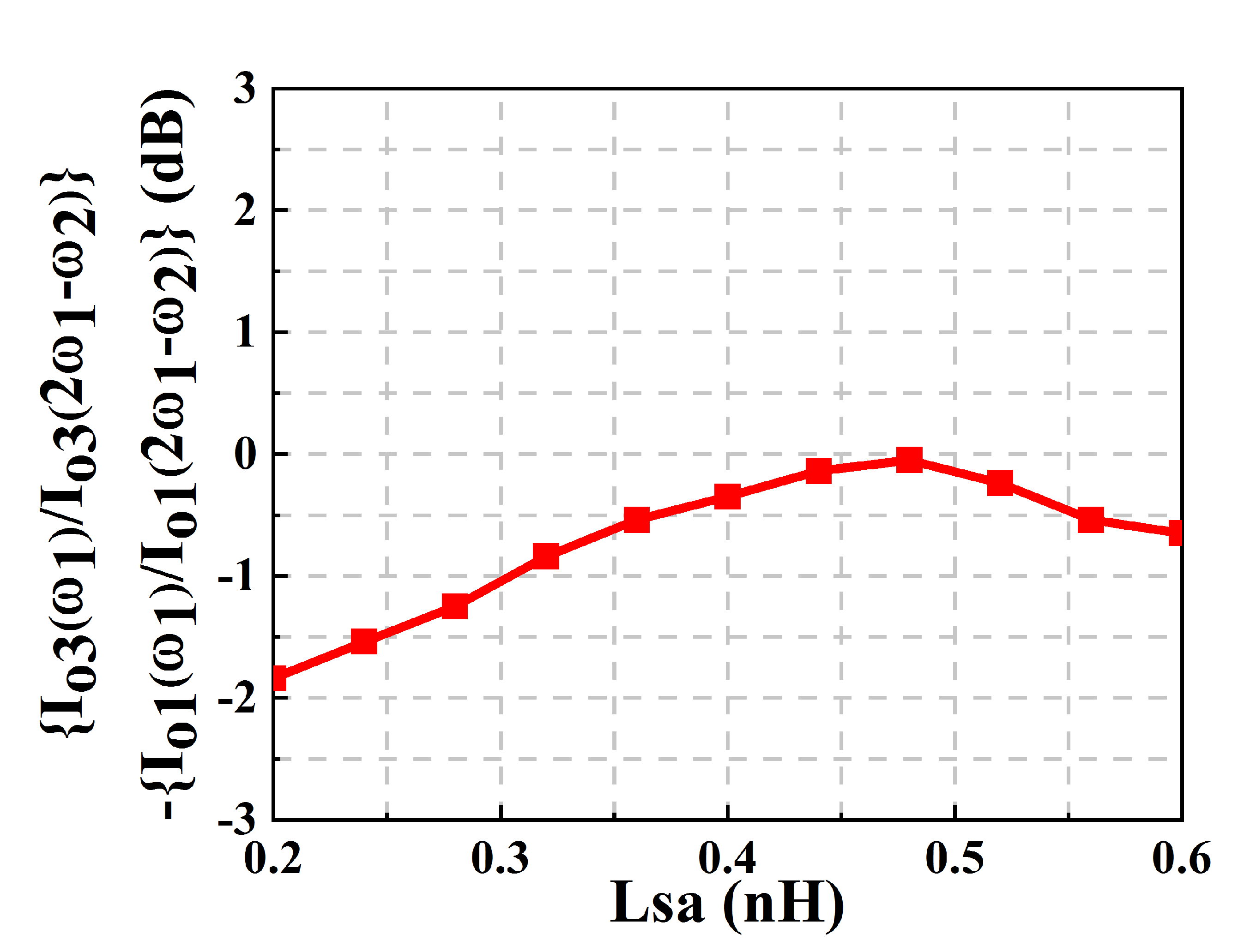
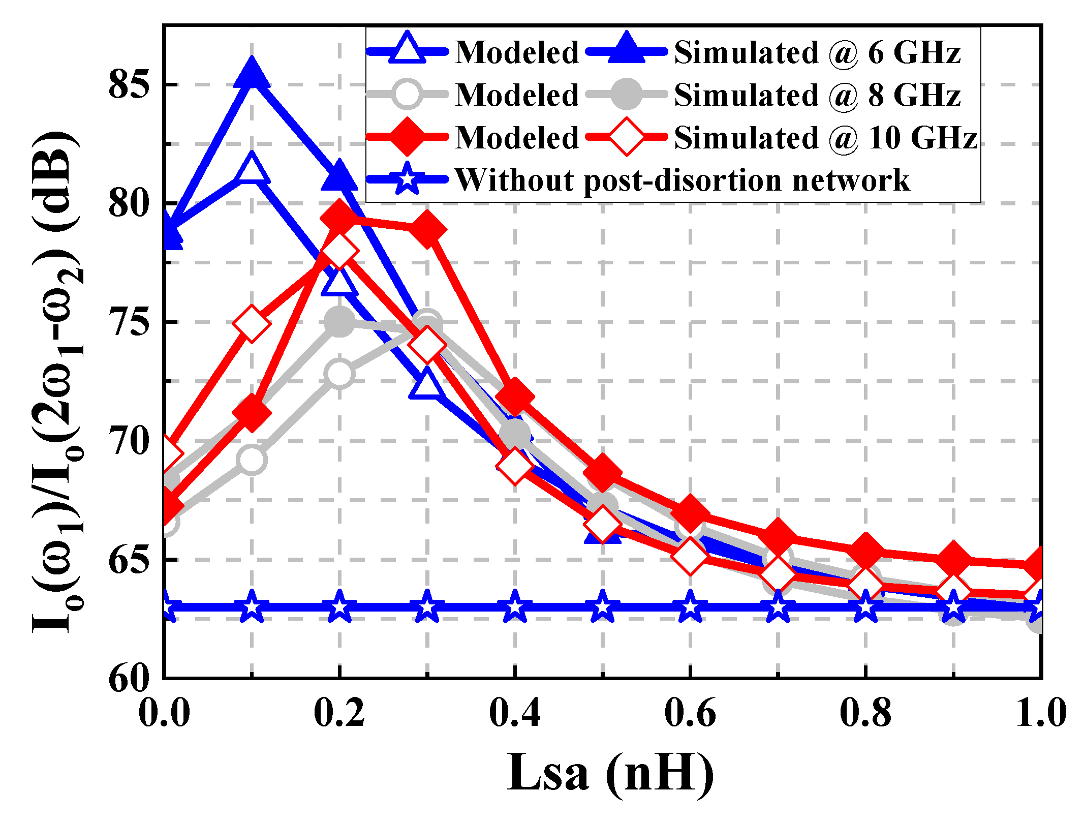
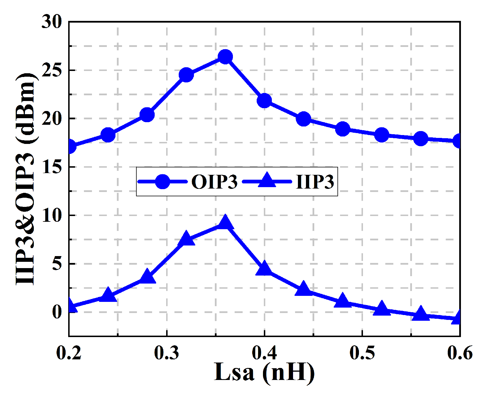
By augmenting an auxiliary , can be enhanced at high frequency, which results in improved numerator in Equation (15a). One the other hand, according to above equations, the third-order nonlinearity of the main and auxiliary transistor , show complicated characteristics as frequency increases. and can be obtained based on above equations and can be calculated based on Equation (15a). To validate the proposed method, we compare the calculated and simulated normalized third-order intermodulation distortion (linearity improvement) of the combined current versus and frequency with and without modified post-distortion network based on the above equations. It can be shown in Figure 11 that can be boosted by approximately 15 dB by choosing appropriate . The linearity enhancement versus inductor is simulated at 12 GHz as shown in Figure 12. According to simulated results, the IIP3 and OIP3 can be boosted by about 10 dB with proper inductance value. Here, we explain the cancellation mechanism by turning to vector diagram. From Figure 13, ideally, the third order nonlinearity , generated by , is out of phase, which results in maximum IIP3. However, as frequency increases, is non-collinear with , which degrades the distortion cancellation. To improve the IIP3 at high frequency region, auxiliary inductor is placed at the source node of transistor . At low frequency, by augmenting the auxiliary inductor , the third-order nonlinearity will rotate clockwise, with enhanced amplitude. This will result in degraded IIP3 performance compared with conventional post-distortion network. At the medium frequency range, the third-order nonlinearity still rotate clockwise. However, the amplitude will decrease with increasing value of . By choosing a proper value, ideally, the vector of will be collinear with with the out-of-phase state. Then, the IIP3 improvement can be achieved. In the high frequency range, as shown in Figure 13, the sum of the two vector and will increase by augmenting the . However, on the other hand, will increase the first-order current component. As a result, the IIP3 can be improved effectively compared with the conventional post-distortion method.
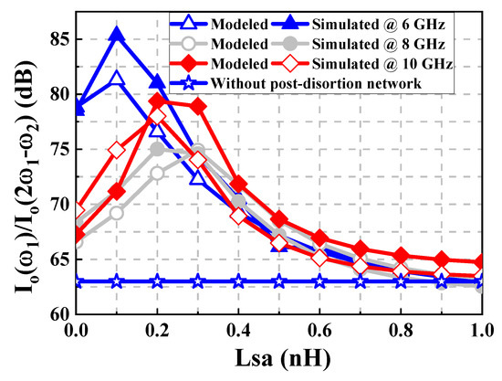
Figure 11.
Comparison of calculated and simulated normalized third-order intermodulation distortion (linearity improvement) of the combined current versus and frequency with and without modified post-distortion network based on the above equations.

Figure 12.
Simulated IIP3 and OIP3 versus of the proposed LNA.

Figure 13.
(a) Conceptual nonlinear cancellation mechanism; (b) and vector diagram as increases in a low frequency range; (c) and vector diagram as increase at medium frequency range; (d) and vector diagram as increases in the high frequency range.
3. Experimental Results
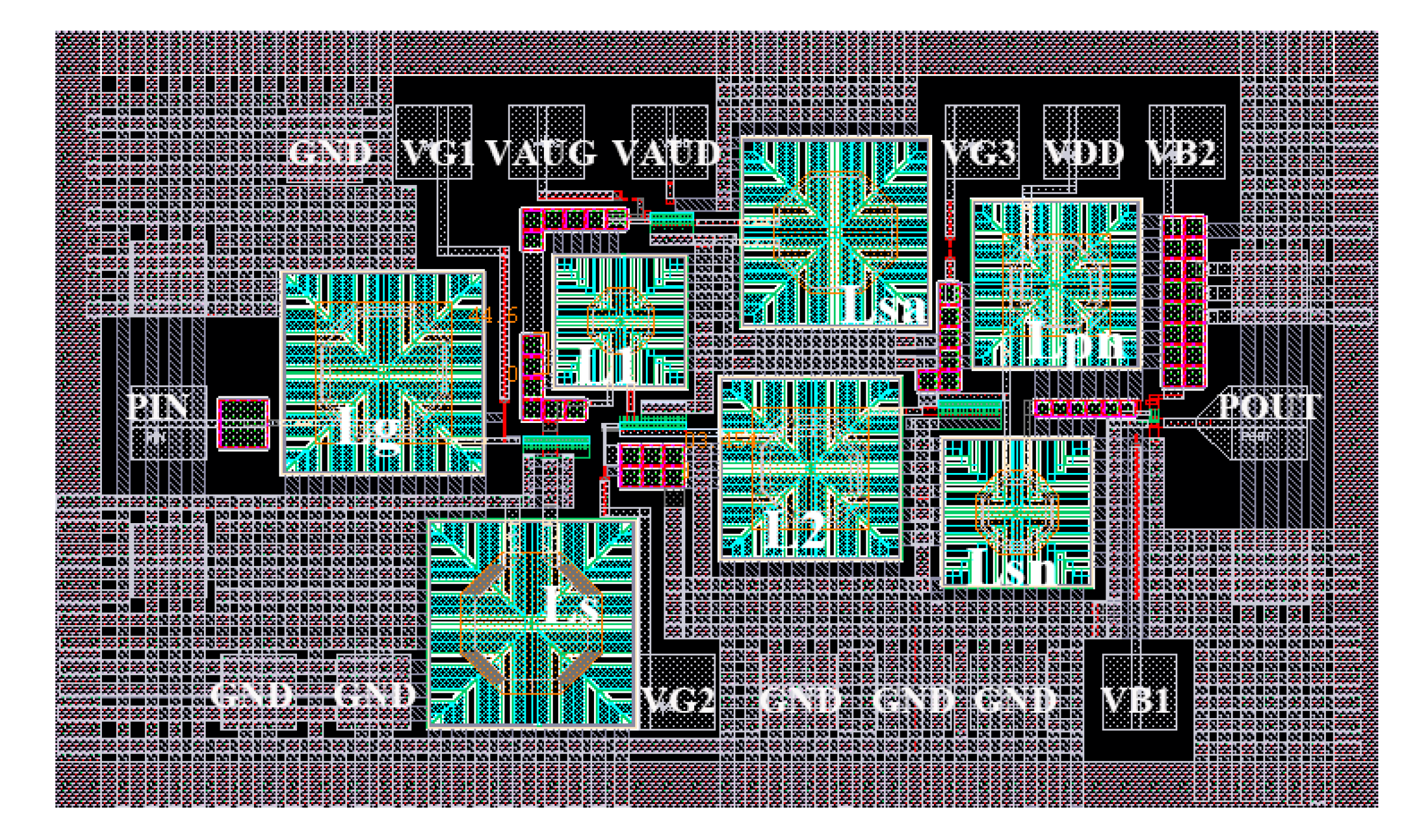
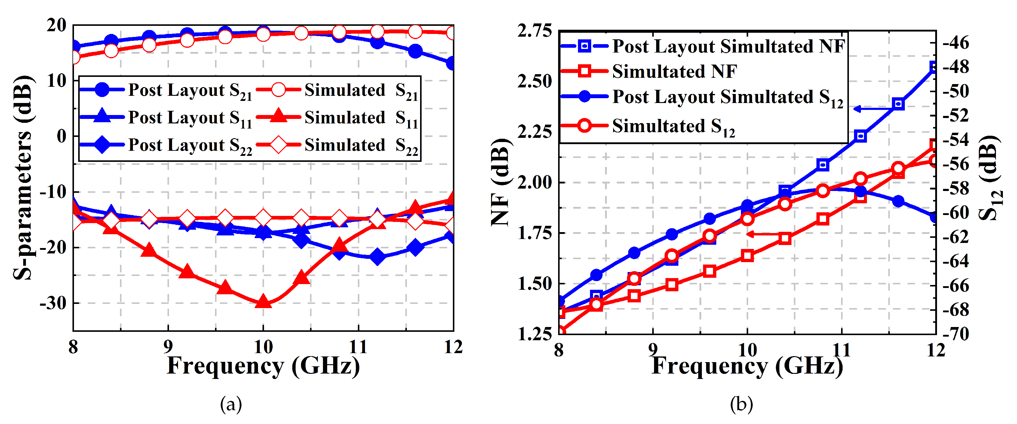
Figure 14 shows a complete layout of the proposed LNA in a 130 nm CMOS process. To verify the designs, the bias circuit is made separately and not included in the main circuits of the proposed LNAs [5,12,22]. The simulated results of the S-parameters are shown in Figure 15. From Figure 15a, it is observed that the proposed LNA achieves good input matching over the desired band. The simulated shows a flat power gain over a frequency of 8–12 GHz due to a dual-resonant network. However, the post layout simulation result shows that degrades at a high frequency. The deviation of the power gain is caused by the parasitic capacitance of the layout at the drain node of transistor . The simulated NFs are shown in Figure 15b. The modified post-distortion network contributes its own noise according to the noise analysis and results in increased NF.
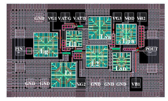
Figure 14.
Layout of the proposed LNA.
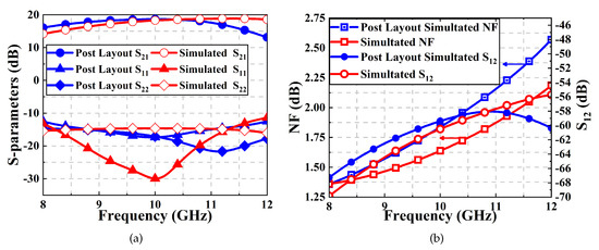
Figure 15.
(a) Simulated S-parameters of the proposed LNA; (b) simulated NF and reverse isolation.
In Figure 16, the IIP3 and OIP3 are simulated by a two-tone test from 8–12 GHz. Compared with the conventional post-distortion network, the proposed technique can improve both IIP3 and OIP3 as frequency increases. According to the simulated result, the IIP3 of the proposed LNA varies from −3 dBm to +8 dBm over the X-band frequency range.
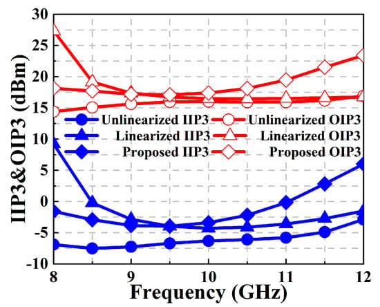
Figure 16.
Simulated IIP3 and OIP3 based on the nonlinearized, conventional linearized post-distortion, and proposed post-distortion topology.
The designed LNA has been analyzed for various performance corners and process voltage-temperature (PVT) variations to study the robustness of the design. The process and device mismatch analyses for the proposed LNA are performed using Monte Carlo (MC) simulations for 200 samples of random mismatches. Figure 17 illustrates the temperature and corner changes on , and NF versus frequency. In general, the corner and temperature variations have little effects on the input matching and gain flatness. As shown in Figure 17, process variations at FF corner result in an increased gain and decreased NF due to the increase in the DC current. In the SS corner, the gain falls and NF rises due to a lower DC current. Figure 18 shows the Monte Carlo simulation distributions for 200 sample values of , and NF at 10 GHz and IIP3. The statistical behavior of the gain and NF are plotted in Figure 18a,b, respectively. The LNA has the mean of 18.2 dB with standard deviation of 0.32 dB. Similarly, the mean and the standard deviations of the NF at 10 GHz are 1.65 dB and 0.125 dB, respectively. From Figure 18c, the mean value of IIP3 is 2.65 dBm, where the standard deviation is 1.9 dBm. The majority of the results of , NF are within one-sigma () and IIP3 of limit in the distribution will correspond to a high yield post-fabrication.

Figure 17.
PVT simulation results of S-parameters and NF of the proposed LNA. (a) process corner simulations at TT–FF–SS of S-parameters; (b) process corner simulations at TT–FF–SS of NF; (c) temperature variation simulations of S-parameters; (d) temperature variation simulations of NF.

Figure 18.
Monte Carlo simulations of the proposed LNA for 200 samples. (a) gain; (b) noise figure; (c) IIP3.
In order to evaluate the overall performance of various LNAs, diverse figure-of-merits (FOM) are employed. FOM1 is the ratio of Gain and BW to P and NF. It is more commonly applied for comparing among low power LNAs, which does not include linearity. FOM2 introduces IIP3 in consideration of linearity effects. It is used to compare linearized LNAs [13,23,24]. Table 2 mainly shows a comparison of the cascode, two stage and triple-cascode LNA configuration. The proposed single stage triple-cascode LNA, with moderate power consumption, achieves enhanced bandwidth, flat gain, and excellent noise performance due to the modified input matching and dual-resonant network. On the other hand, the performance of the proposed LNA is competitive to that of noise cancelling LNA. Although the proposed LNA is implemented without the state-of art process, the proposed LNA achieves competitive FOM1 and FOM2:

Table 2.
Performance comparison with other references.
4. Conclusions
In this paper, the proposed X-band linearized LNA with extra low power consumption is designed. The proposed post-distortion network utilizes the auxiliary transistor operated in the weak inversion region, which dissipates low power consumption. The graphical explanation of the post distortion mechanism is discussed explicitly. Compared with the conventional post distortion technique, the proposed auxiliary network can improve the at a high frequency. Furthermore, due to the dual-resonant network, the bandwidth can be extended. The simulation results show the good performance of the proposed LNA and confirm the reliability of proposed mathematical derivations.
Author Contributions
Conceptualization, C.C. and Z.W.; methodology, C.C., Y.L.; software, C.C.; validation, C.C., H.Z.; formal analysis, C.C.; investigation, C.C. and Z.W.; resources, C.C.; data curation, C.C.; writing—original draft preparation, C.C.; writing—review and editing, C.C.; U.Y.; supervision, X.L.; project administration, X.L.; funding acquisition, X.L. All authors have read and agreed to the published version of the manuscript.
Funding
This work is supported by the project 61601050 from the National Natural Science Foundation of China (NSFC). This work is also supported by BUPT Excellent Ph.D. Students Foundation (CX2020302) from Beijing University of Posts and Telecommunications.
Conflicts of Interest
The authors declare no conflict of interest.
Appendix A. Numerator and Denominator for Bandwidth Calculation
According to the input impedance, the numerator and denominator can be calculated as
Appendix B. Volterra Expansion Analysis
To solve the first, second, and third Volterra series kernels in the above equations, we can utilize Kirchhoff’s circuit law (KCL) as the following:
Based on the above equations, the Volterra series kernels can be derived as
References
- Bevilacqua, A.; Niknejad, A.M. An ultrawideband CMOS low noise amplifier for 3.1–10.6 GHz wireless receivers. IEEE J. Solid-State Circuits 2004, 39, 2259–2268. [Google Scholar] [CrossRef]
- Ismail, A.; Abidi, A.A. A 3–10 GHz low noise amplifier with wideband LC-ladder matching network. IEEE J. Solid-State Circuits 2004, 39, 2269–2277. [Google Scholar] [CrossRef]
- Chen, K.; Lu, J.; Chen, B.; Liu, S. An ultra-wide-band 0.4–10 GHz LNA in 0.18 um CMOS. IEEE Trans. Circuits Syst. II Express Briefs 2007, 54, 217–221. [Google Scholar] [CrossRef]
- Shim, Y.; Kim, C.; Lee, J.; Lee, S. Design of Full Band UWB Common-Gate LNA. IEEE Microw. Wirel. Compon. Lett. 2007, 17, 721–723. [Google Scholar] [CrossRef]
- Chen, W.; Liu, G.; Zdravko, B.; Niknejad, A.M. A highly linear broadband CMOS LNA employing noise and distortion cancellation. IEEE J. Solid-State Circuits 2008, 43, 1164–1176. [Google Scholar] [CrossRef]
- Zhang, H. Sanchez-Sinencio Linearization Techniques for CMOS Low Noise Amplifiers: A Tutorial. IEEE Trans. Circuits Syst. I Regul. Pap. 2011, 58, 22–36. [Google Scholar] [CrossRef]
- Aparin, V.; Brown, G.; Larson, L.E. Linearization of CMOS LNAs via optimum gate biasing. In Proceedings of the 2004 IEEE International Symposium on Circuits and Systems, Vancouver, BC, Canada, 23–26 May 2004; Volume IV, pp. 748–751. [Google Scholar]
- Amirabadi, A.; Zokaei, A.; Bagheri, M.; Alirezazadeh, F. Highly linear wide-band differential LNA using active feedback as post distortion. In Proceedings of the 2015 IEEE International Symposium on Circuits and Systems (ISCAS), Lisbon, Portugal, 24–27 May 2015. [Google Scholar]
- Kim, T.W.; Kim, B.; Lee, K. Highly linear receiver front-end adopting MOSFET transconductance linearization by multiple gated transistors. IEEE J. Solid-State Circuits 2004, 39, 223–229. [Google Scholar] [CrossRef]
- Guo, B.; Li, X. A 1.6–9.7 GHz CMOS LNA Linearized by Post Distortion Technique. IEEE Microw. Wirel. Compon. Lett. 2013, 23, 608–610. [Google Scholar] [CrossRef]
- El-Khatib, Z.; Tlili, B.; Amer, M.; Fuller, L. CMOS cascode LNA with post-distortion cancellation linearizer for wireless communications. In Proceedings of the 2017 International Conference on Electrical and Computing Technologies and Applications (ICECTA), Ras Al Khaimah, United Arab Emirates, 21–23 November 2017. [Google Scholar]
- Kim, T.-S.; Kim, B.-S. Post-linearization of cascode CMOS low noise amplifier using folded PMOS IMD sinker. IEEE Microw. Wirel. Compon. Lett. 2006, 16, 182–184. [Google Scholar]
- Zhang, H.; Fan, X.; Sinencio, E.S. A Low-Power, Linearized, Ultra-Wideband LNA Design Technique. IEEE J. Solid-State Circuits 2009, 44, 320–330. [Google Scholar] [CrossRef]
- Aparin, V.; Larson, L.E. Modified derivative superposition method for linearizing FET low-noise amplifiers. IEEE Trans. Microw. Theory Tech. 2005, 53, 571–581. [Google Scholar] [CrossRef]
- Shaeffer, D.K.; Lee, T.H. A 1.5 V, 1.5 GHz CMOS low-noise amplifier. IEEE J. Solid-State Circuits 1997, 32, 745–759. [Google Scholar] [CrossRef]
- Huang, B.; Lin, K.; Wang, H. Millimeter-Wave Low Power and Miniature CMOS Multicascode Low-Noise Amplifiers with Noise Reduction Topology. IEEE Trans. Microw. Theory Tech. 2009, 57, 3049–3059. [Google Scholar] [CrossRef]
- Kargaran, E.; Madadi, B. Design of a novel dual-band concurrent CMOS LNA with current reuse topology. In Proceedings of the 2010 International Conference on Networking and Information Technology, Manila, Philippines, 11–12 June 2010; pp. 386–388. [Google Scholar]
- Dai, R.; Zheng, Y.; He, J.; Kong, W.; Zou, S. A 2.5-GHz 8.9-dBm IIP3 current-reused LNA in 0.18-μm CMOS technology. In Proceedings of the 2014 IEEE International Symposium on Radio-Frequency Integration Technology, Hefei, China, 27–30 August 2014; pp. 1–3. [Google Scholar]
- Davulcu, M.; Çalışkan, C.; Kalyoncu, İ.; Gurbuz, Y. An X-Band SiGe BiCMOS Triple-Cascode LNA With Boosted Gain and P1dB. IEEE Trans. Circuits Syst. II Express Briefs 2018, 65, 994–998. [Google Scholar] [CrossRef]
- Kim, N.; Aparin, V.; Barnett, K.; Persico, C. A cellular-band CDMA 0.25 μm CMOS LNA linearized using active post-distortion. IEEE J. Solid-State Circuits 2006, 41, 1530–1534. [Google Scholar] [CrossRef]
- Kim, T.W. A Common-Gate Amplifier With Transconductance Nonlinearity Cancellation and Its High-Frequency Analysis Using the Volterra Series. IEEE Trans. Microw. Theory Tech. 2009, 57, 1461–1469. [Google Scholar] [CrossRef]
- Lo, Y.; Kiang, J. Design of Wideband LNAs Using Parallel-to-Series Resonant Matching Network Between Common-Gate and Common-Source Stages. IEEE Trans. Microw. Theory Tech. 2011, 59, 2285–2294. [Google Scholar] [CrossRef]
- Madan, A.; McPartlin, M.J.; Masse, C.; Vaillancourt, W.; Cressler, J.D. A 5 GHz 0.95 dB NF Highly Linear Cascode Floating-Body LNA in 180 nm SOI CMOS Technology. IEEE Microw. Wirel. Compon. Lett. 2012, 22, 200–202. [Google Scholar] [CrossRef]
- Ramzan, R.; Zafar, F.; Arshad, S.; Wahab, Q. Figure of merit for narrowband, wideband and multiband LNAs. Int. J. Electron. 2012, 99, 1603–1610. [Google Scholar] [CrossRef]
- Arshad, S.; Ramzan, R.; Muhammad, K.; Wahab, Q.U. A sub-10 mW, noise cancelling, wideband LNA for UWB applications. AEU Int. J. Electron. Commun. 2015, 69, 109–118. [Google Scholar] [CrossRef]
- Li, N.; Feng, W.; Li, X. A CMOS 3–12-GHz Ultrawideband Low Noise Amplifier by Dual-Resonance Network. IEEE Microw. Wirel. Compon. Lett. 2017, 27, 383–385. [Google Scholar] [CrossRef]
- Lin, Y.S.; Wang, C.C.; Lee, G.L.; Chen, C.C. High-Performance Wideband Low-Noise Amplifier Using Enhanced π-Match Input Network. IEEE Microw. Wirel. Compon. Lett. 2014, 24, 200–202. [Google Scholar] [CrossRef]
- Rastegar, H.; Ryu, J.Y. A Broadband Low Noise Amplifier with Built-in Linearizer in 0.13 μm CMOS process. Microelectron. J. 2015, 46, 698–705. [Google Scholar] [CrossRef]
- çağlar, A.; Yelten, M.B. A 180-nm X-Band Cryogenic CMOS LNA. IEEE Microw. Wirel. Compon. Lett. 2020, 30, 395–398. [Google Scholar] [CrossRef]
- Reza, S.; Roy, A. 3–5 GHz multifinger CMOS LNA using a simultaneous noise and impedance matching technique by a significant reduction of broadband impedance variation of metal–oxide–semiconductor field effect transistor. IET Circuits Devices Syst. 2020, 14, 956–965. [Google Scholar] [CrossRef]
Publisher’s Note: MDPI stays neutral with regard to jurisdictional claims in published maps and institutional affiliations. |
© 2021 by the authors. Licensee MDPI, Basel, Switzerland. This article is an open access article distributed under the terms and conditions of the Creative Commons Attribution (CC BY) license (http://creativecommons.org/licenses/by/4.0/).

