
A Triple-Cascode X-Band LNA Design with Modified Post-Distortion Network

 ,
,
Abstract
:1. Introduction
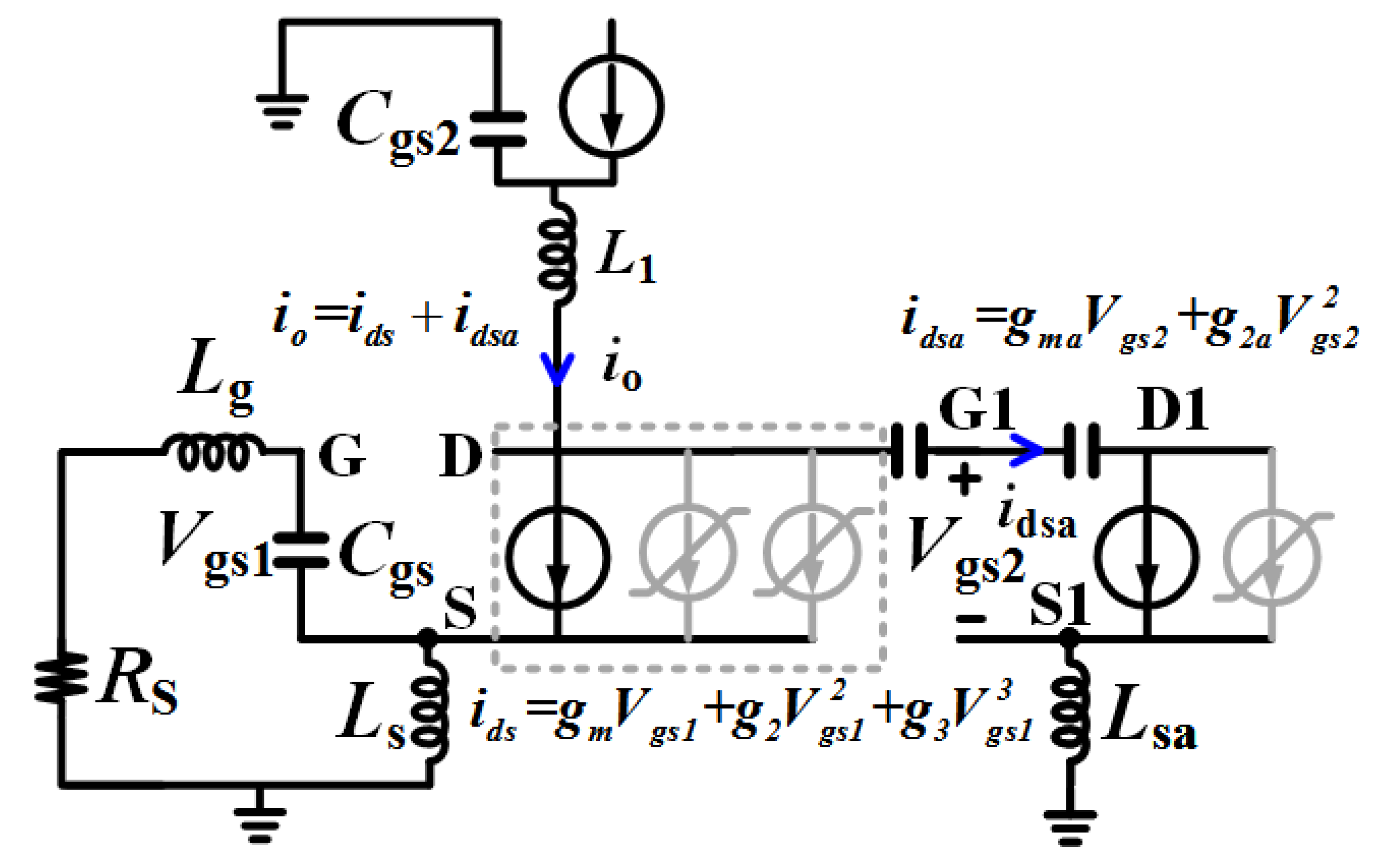
2. Triple-Cascode LNA with a Modified Post-Distortion Network Analysis
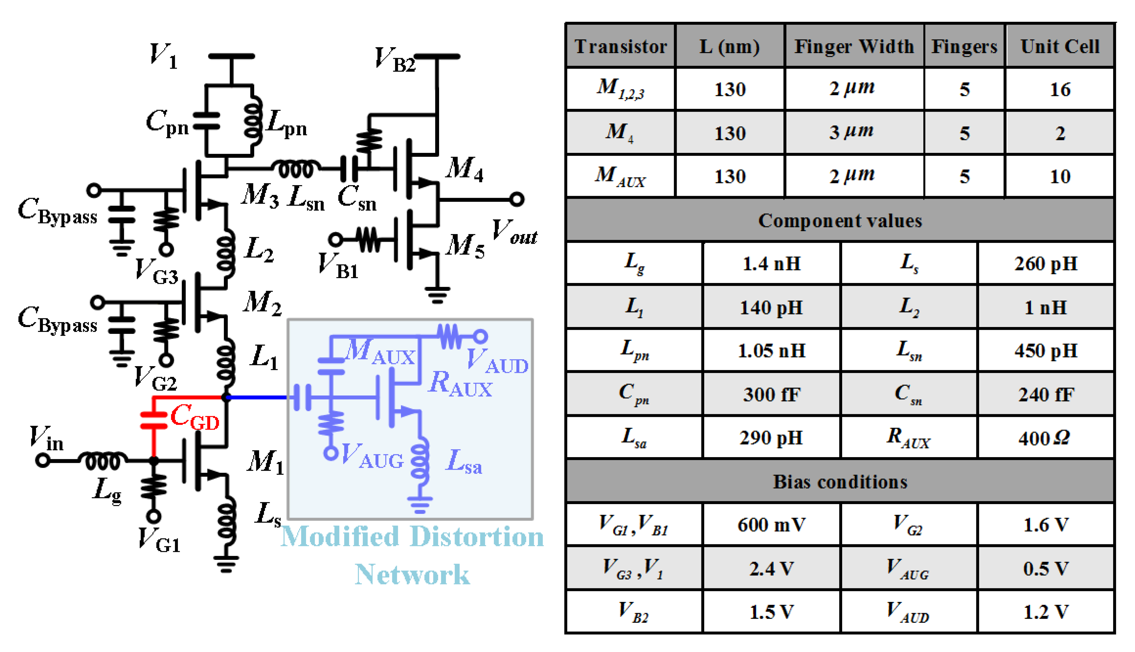
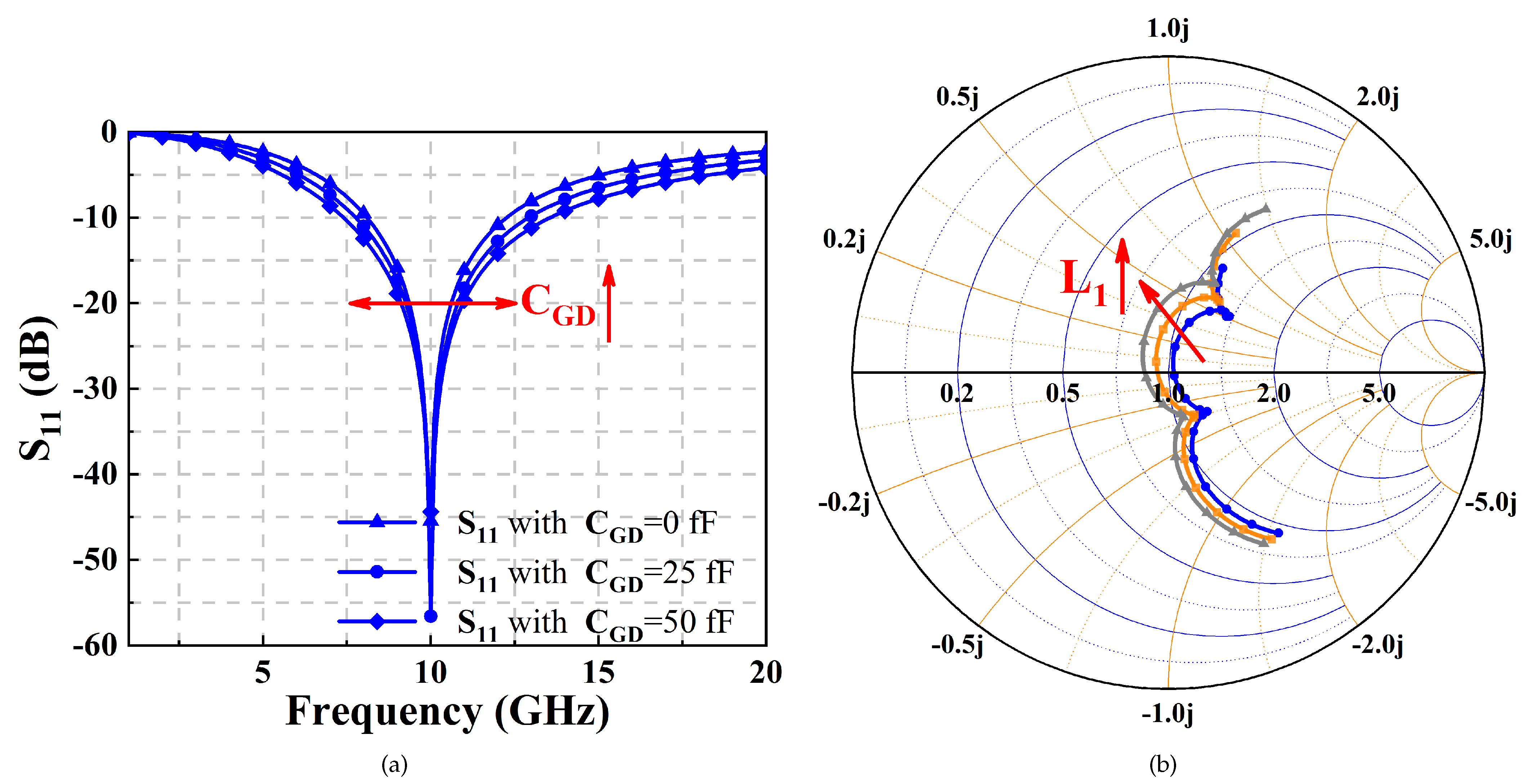
2.1. Input Matching Analysis
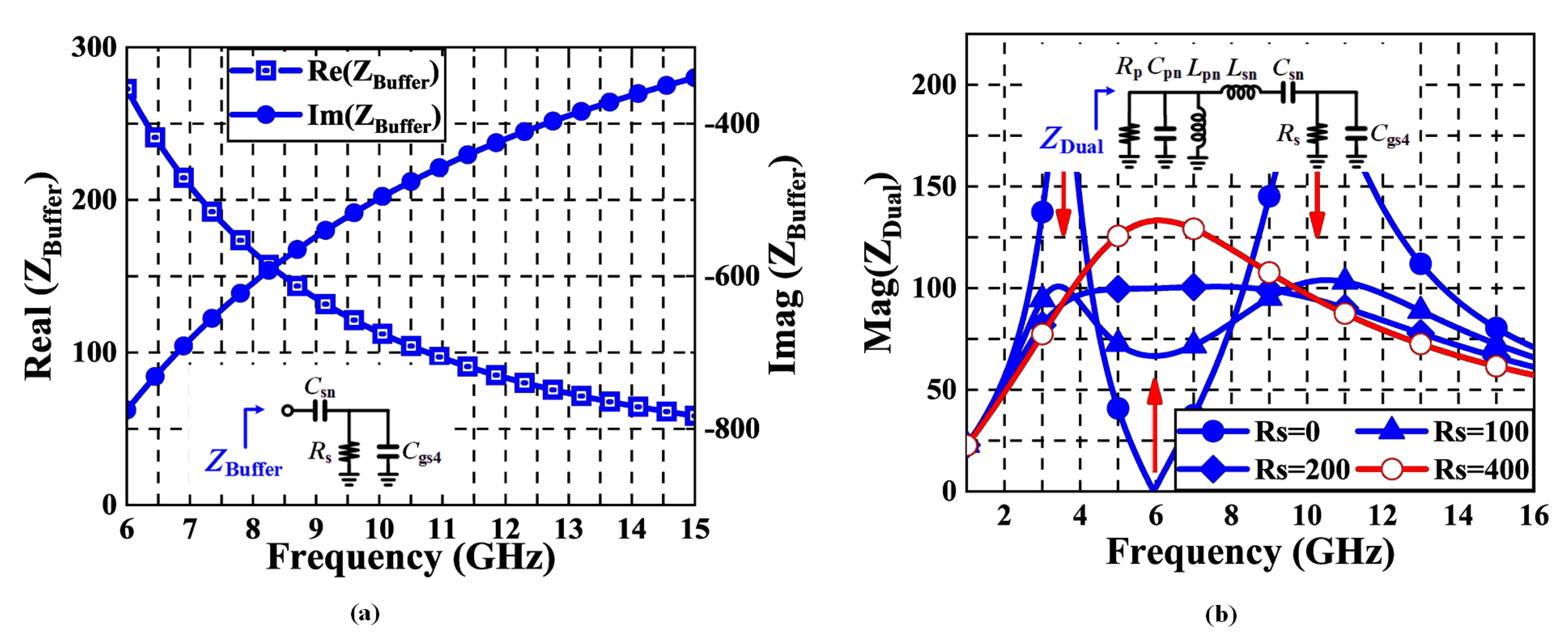
2.2. Gain Analysis
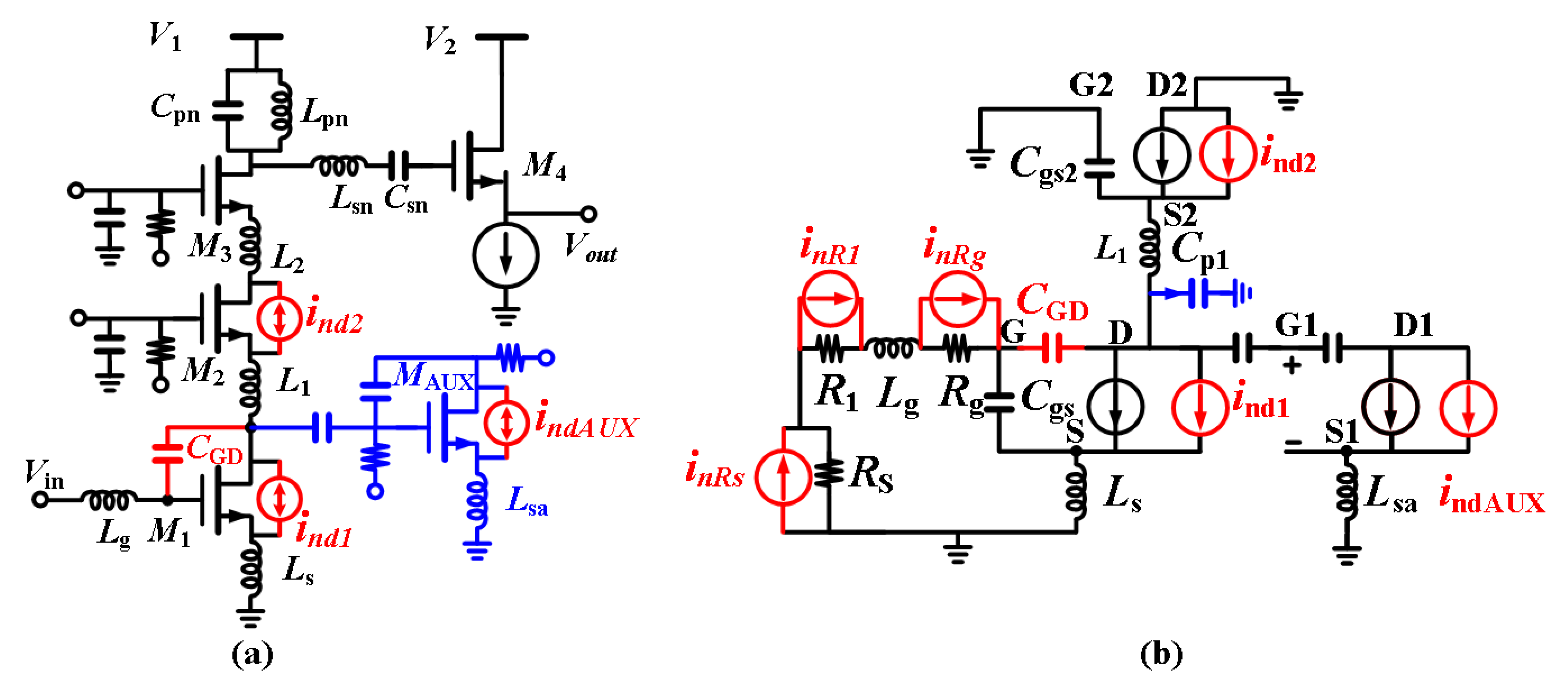
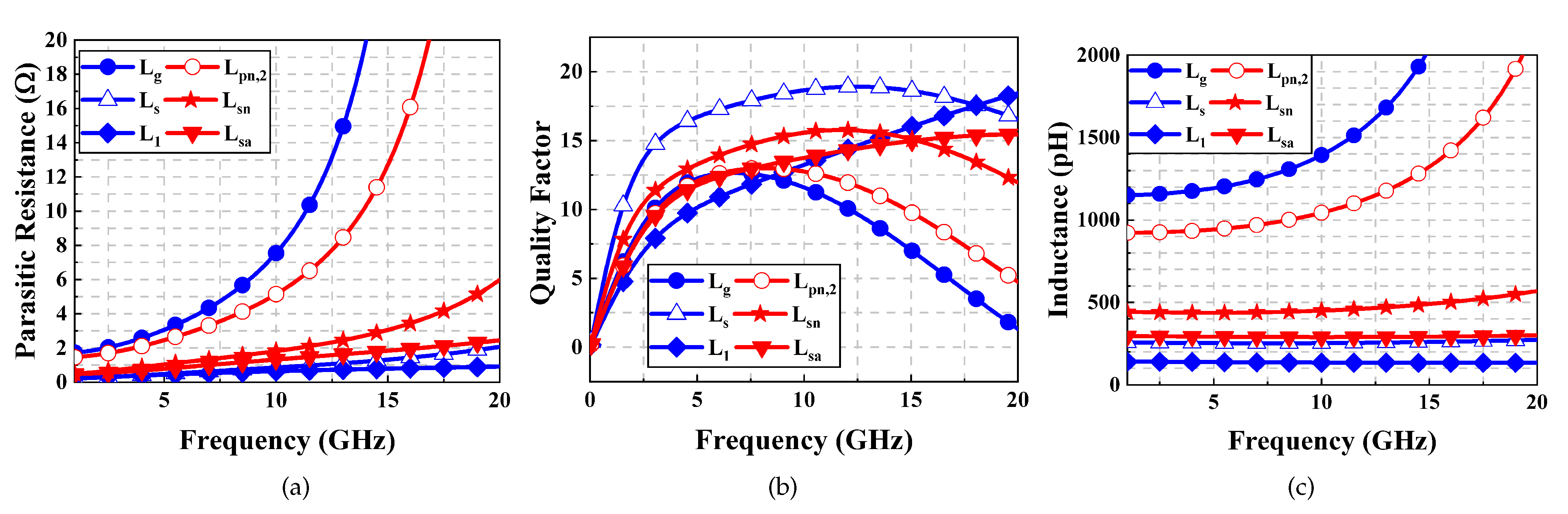
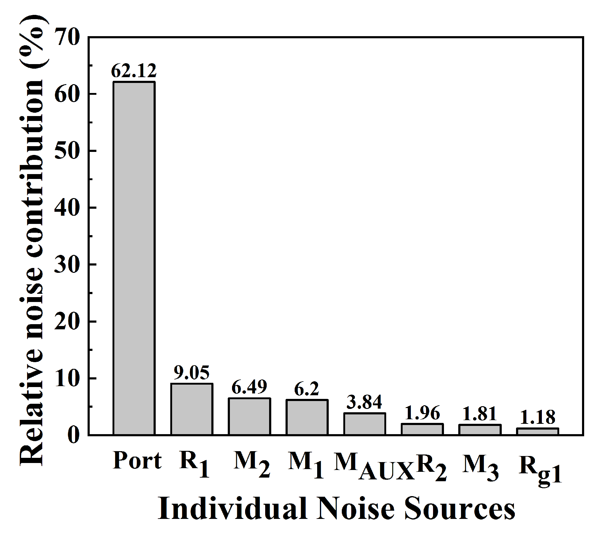
2.3. Noise Analysis
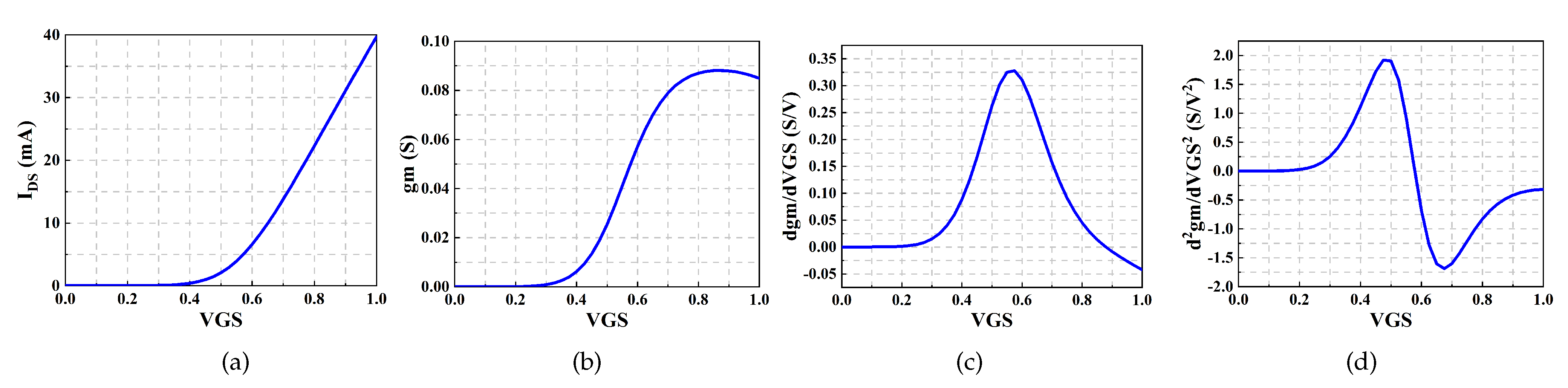
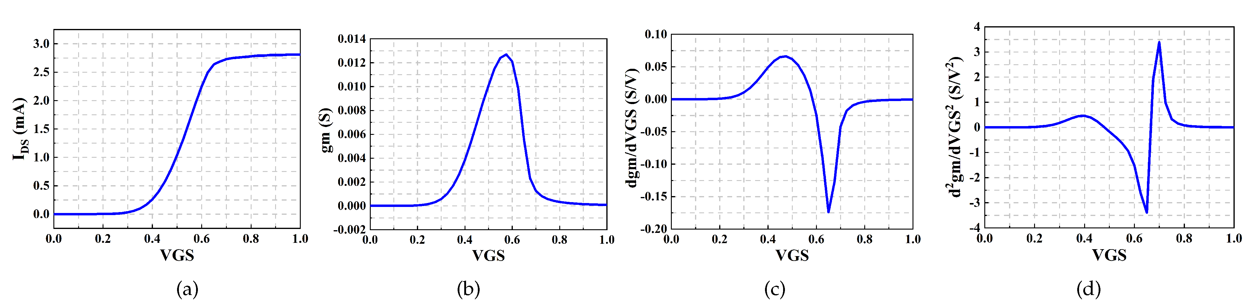
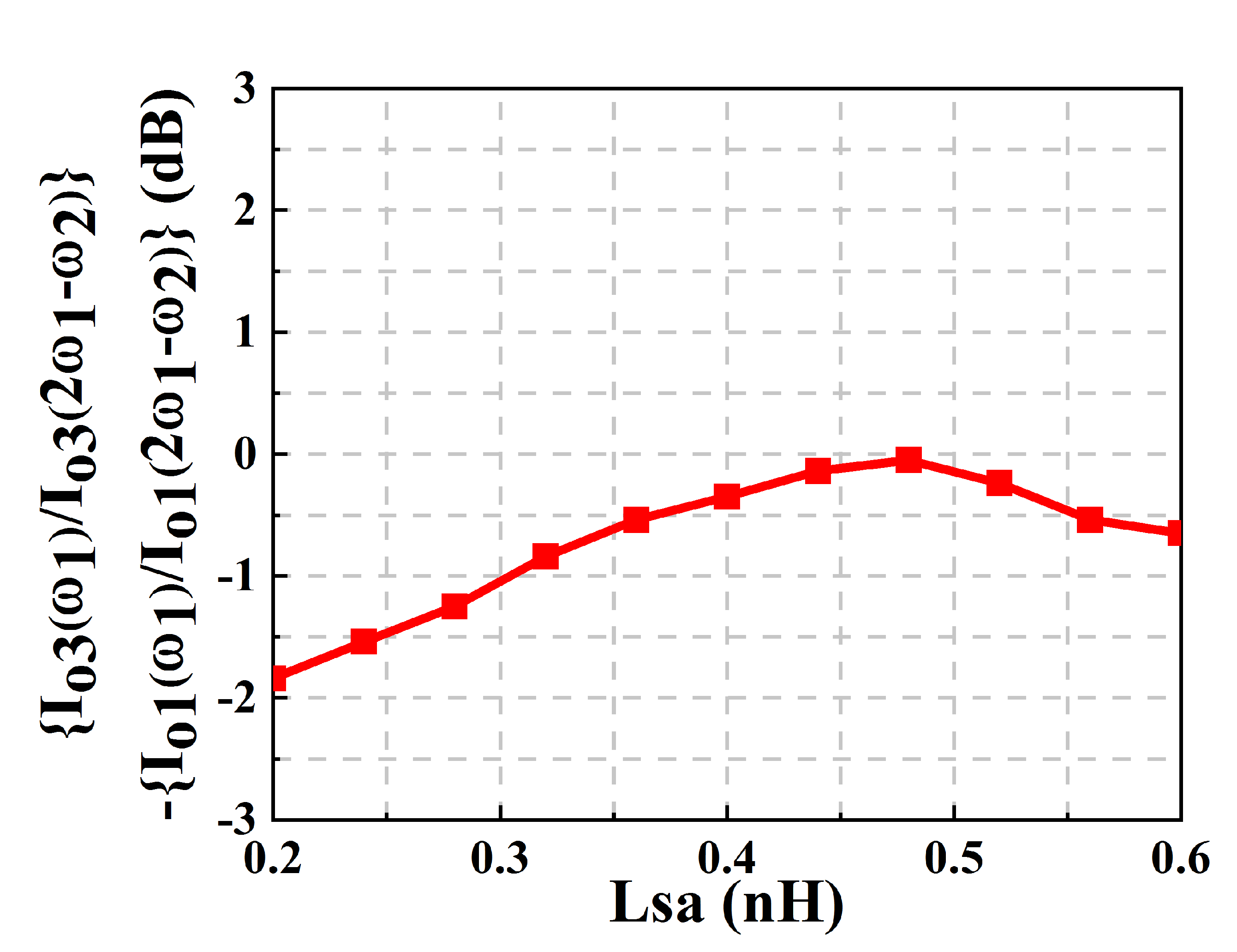
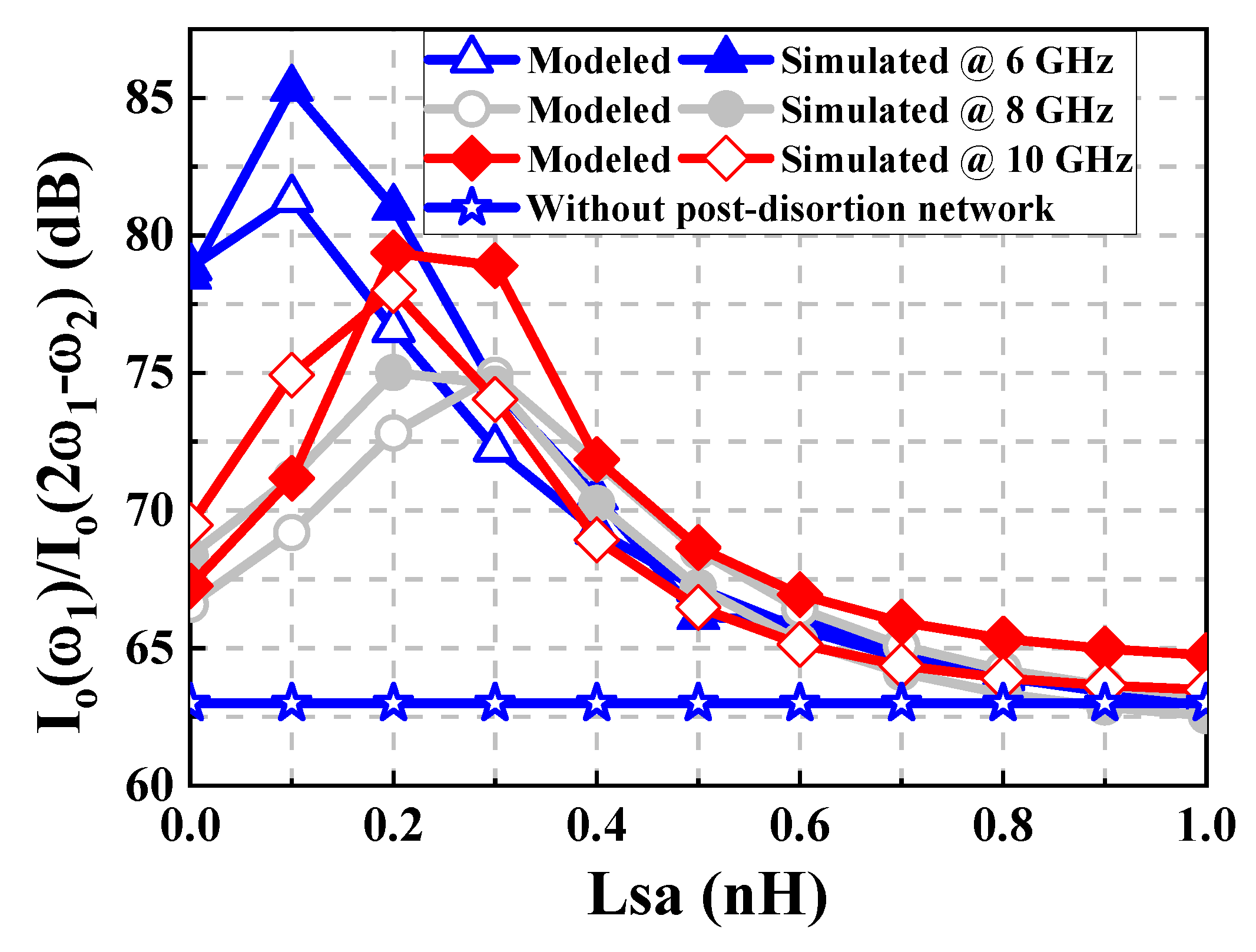
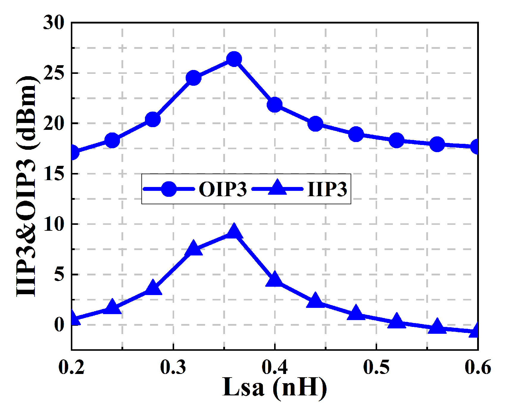
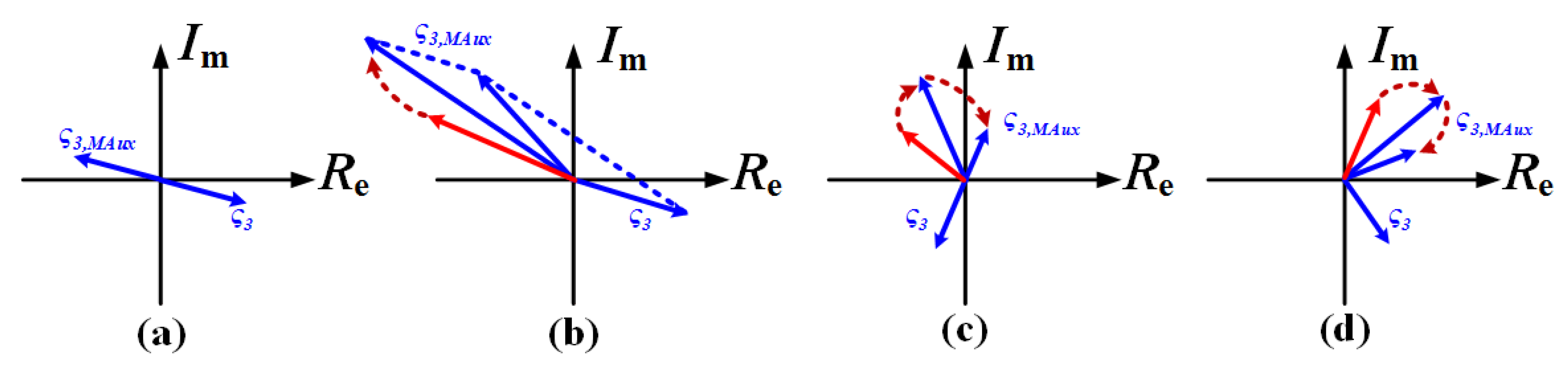
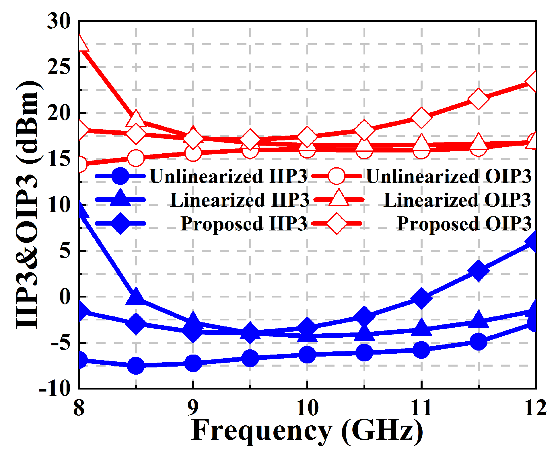
2.4. Linearity Analysis
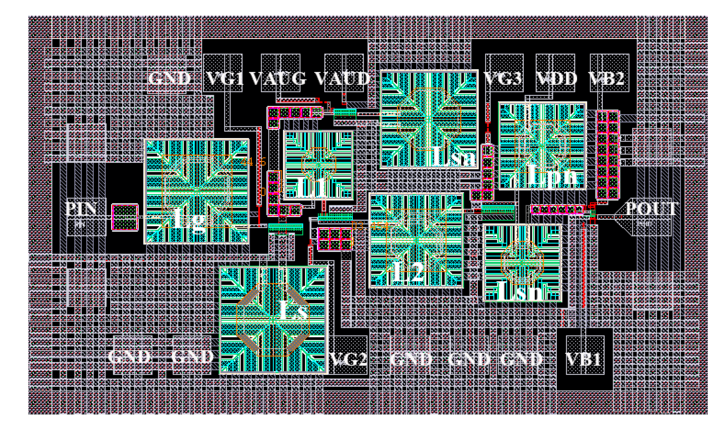
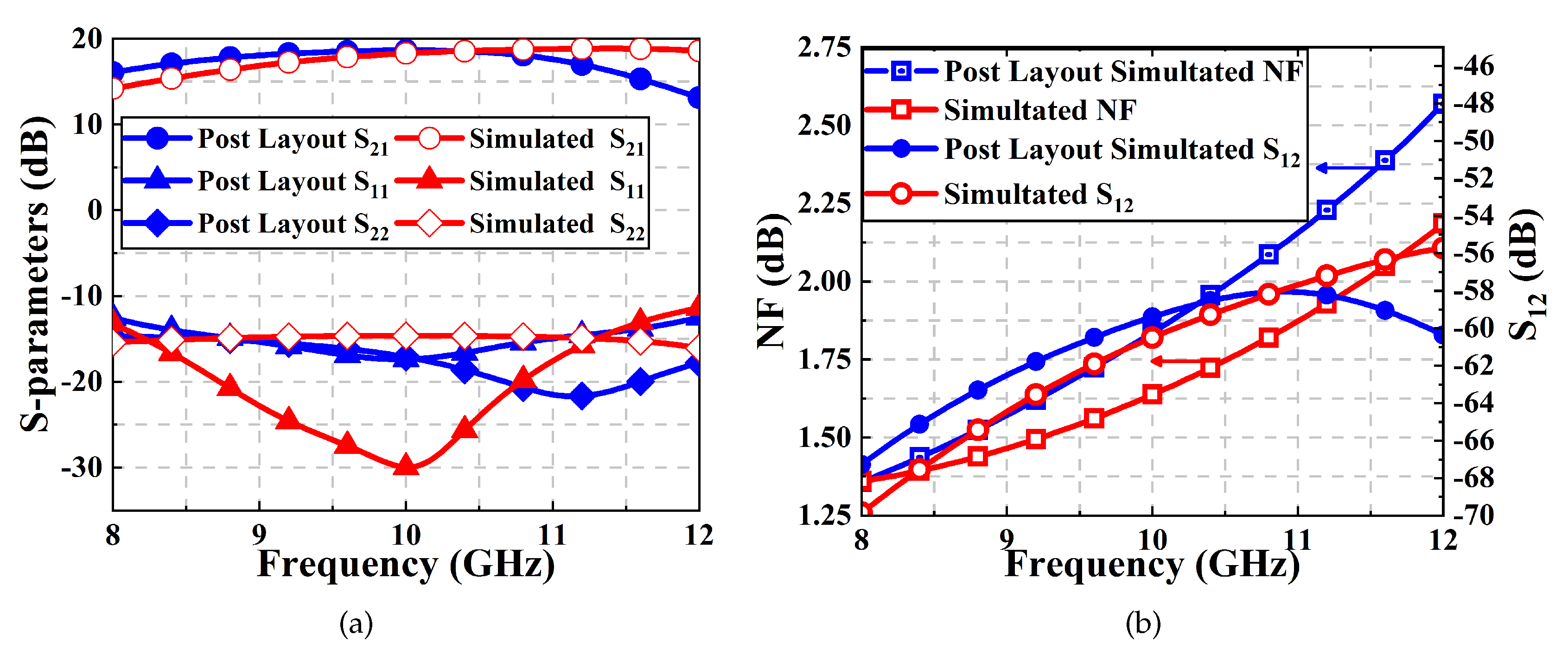
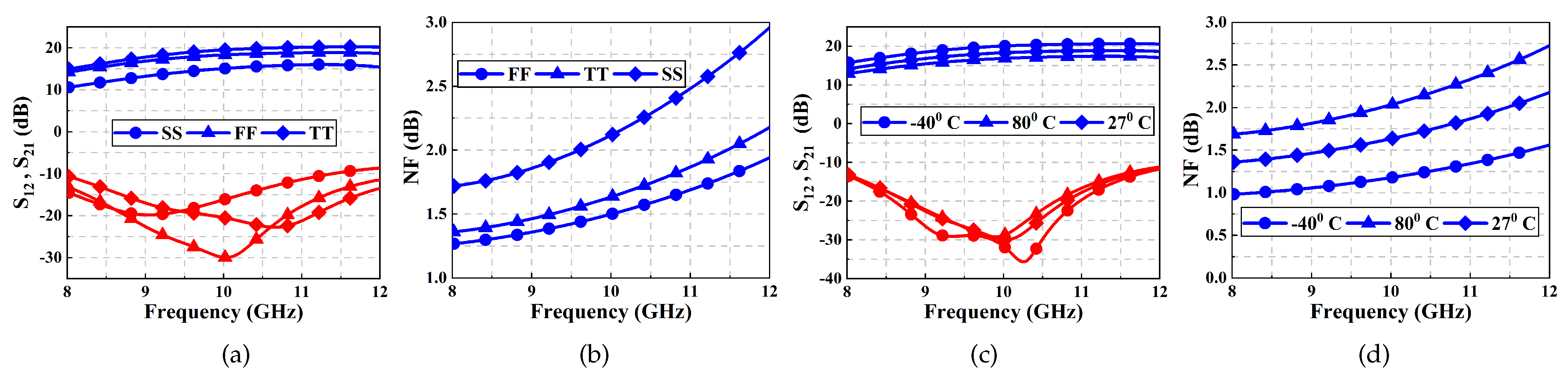
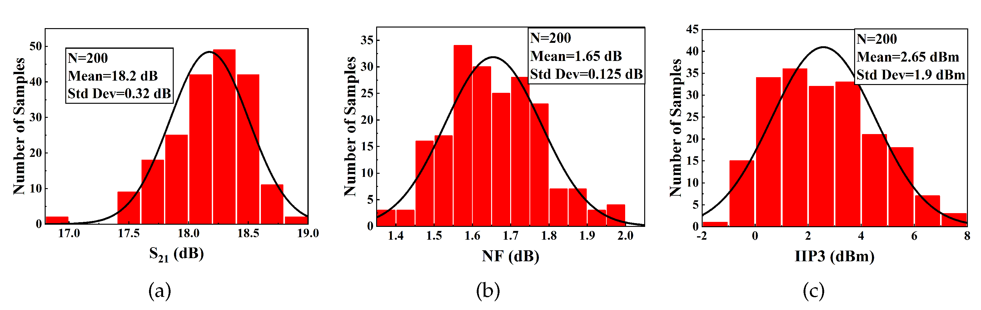
3. Experimental Results
4. Conclusions
Author Contributions
Funding
Conflicts of Interest
Appendix A. Numerator and Denominator for Bandwidth Calculation
Appendix B. Volterra Expansion Analysis
References
- Bevilacqua, A.; Niknejad, A.M. An ultrawideband CMOS low noise amplifier for 3.1–10.6 GHz wireless receivers. IEEE J. Solid-State Circuits 2004, 39, 2259–2268. [Google Scholar] [CrossRef]
- Ismail, A.; Abidi, A.A. A 3–10 GHz low noise amplifier with wideband LC-ladder matching network. IEEE J. Solid-State Circuits 2004, 39, 2269–2277. [Google Scholar] [CrossRef]
- Chen, K.; Lu, J.; Chen, B.; Liu, S. An ultra-wide-band 0.4–10 GHz LNA in 0.18 um CMOS. IEEE Trans. Circuits Syst. II Express Briefs 2007, 54, 217–221. [Google Scholar] [CrossRef]
- Shim, Y.; Kim, C.; Lee, J.; Lee, S. Design of Full Band UWB Common-Gate LNA. IEEE Microw. Wirel. Compon. Lett. 2007, 17, 721–723. [Google Scholar] [CrossRef]
- Chen, W.; Liu, G.; Zdravko, B.; Niknejad, A.M. A highly linear broadband CMOS LNA employing noise and distortion cancellation. IEEE J. Solid-State Circuits 2008, 43, 1164–1176. [Google Scholar] [CrossRef]
- Zhang, H. Sanchez-Sinencio Linearization Techniques for CMOS Low Noise Amplifiers: A Tutorial. IEEE Trans. Circuits Syst. I Regul. Pap. 2011, 58, 22–36. [Google Scholar] [CrossRef]
- Aparin, V.; Brown, G.; Larson, L.E. Linearization of CMOS LNAs via optimum gate biasing. In Proceedings of the 2004 IEEE International Symposium on Circuits and Systems, Vancouver, BC, Canada, 23–26 May 2004; Volume IV, pp. 748–751. [Google Scholar]
- Amirabadi, A.; Zokaei, A.; Bagheri, M.; Alirezazadeh, F. Highly linear wide-band differential LNA using active feedback as post distortion. In Proceedings of the 2015 IEEE International Symposium on Circuits and Systems (ISCAS), Lisbon, Portugal, 24–27 May 2015. [Google Scholar]
- Kim, T.W.; Kim, B.; Lee, K. Highly linear receiver front-end adopting MOSFET transconductance linearization by multiple gated transistors. IEEE J. Solid-State Circuits 2004, 39, 223–229. [Google Scholar] [CrossRef]
- Guo, B.; Li, X. A 1.6–9.7 GHz CMOS LNA Linearized by Post Distortion Technique. IEEE Microw. Wirel. Compon. Lett. 2013, 23, 608–610. [Google Scholar] [CrossRef]
- El-Khatib, Z.; Tlili, B.; Amer, M.; Fuller, L. CMOS cascode LNA with post-distortion cancellation linearizer for wireless communications. In Proceedings of the 2017 International Conference on Electrical and Computing Technologies and Applications (ICECTA), Ras Al Khaimah, United Arab Emirates, 21–23 November 2017. [Google Scholar]
- Kim, T.-S.; Kim, B.-S. Post-linearization of cascode CMOS low noise amplifier using folded PMOS IMD sinker. IEEE Microw. Wirel. Compon. Lett. 2006, 16, 182–184. [Google Scholar]
- Zhang, H.; Fan, X.; Sinencio, E.S. A Low-Power, Linearized, Ultra-Wideband LNA Design Technique. IEEE J. Solid-State Circuits 2009, 44, 320–330. [Google Scholar] [CrossRef]
- Aparin, V.; Larson, L.E. Modified derivative superposition method for linearizing FET low-noise amplifiers. IEEE Trans. Microw. Theory Tech. 2005, 53, 571–581. [Google Scholar] [CrossRef]
- Shaeffer, D.K.; Lee, T.H. A 1.5 V, 1.5 GHz CMOS low-noise amplifier. IEEE J. Solid-State Circuits 1997, 32, 745–759. [Google Scholar] [CrossRef] [Green Version]
- Huang, B.; Lin, K.; Wang, H. Millimeter-Wave Low Power and Miniature CMOS Multicascode Low-Noise Amplifiers with Noise Reduction Topology. IEEE Trans. Microw. Theory Tech. 2009, 57, 3049–3059. [Google Scholar] [CrossRef]
- Kargaran, E.; Madadi, B. Design of a novel dual-band concurrent CMOS LNA with current reuse topology. In Proceedings of the 2010 International Conference on Networking and Information Technology, Manila, Philippines, 11–12 June 2010; pp. 386–388. [Google Scholar]
- Dai, R.; Zheng, Y.; He, J.; Kong, W.; Zou, S. A 2.5-GHz 8.9-dBm IIP3 current-reused LNA in 0.18-μm CMOS technology. In Proceedings of the 2014 IEEE International Symposium on Radio-Frequency Integration Technology, Hefei, China, 27–30 August 2014; pp. 1–3. [Google Scholar]
- Davulcu, M.; Çalışkan, C.; Kalyoncu, İ.; Gurbuz, Y. An X-Band SiGe BiCMOS Triple-Cascode LNA With Boosted Gain and P1dB. IEEE Trans. Circuits Syst. II Express Briefs 2018, 65, 994–998. [Google Scholar] [CrossRef]
- Kim, N.; Aparin, V.; Barnett, K.; Persico, C. A cellular-band CDMA 0.25 μm CMOS LNA linearized using active post-distortion. IEEE J. Solid-State Circuits 2006, 41, 1530–1534. [Google Scholar] [CrossRef]
- Kim, T.W. A Common-Gate Amplifier With Transconductance Nonlinearity Cancellation and Its High-Frequency Analysis Using the Volterra Series. IEEE Trans. Microw. Theory Tech. 2009, 57, 1461–1469. [Google Scholar] [CrossRef]
- Lo, Y.; Kiang, J. Design of Wideband LNAs Using Parallel-to-Series Resonant Matching Network Between Common-Gate and Common-Source Stages. IEEE Trans. Microw. Theory Tech. 2011, 59, 2285–2294. [Google Scholar] [CrossRef]
- Madan, A.; McPartlin, M.J.; Masse, C.; Vaillancourt, W.; Cressler, J.D. A 5 GHz 0.95 dB NF Highly Linear Cascode Floating-Body LNA in 180 nm SOI CMOS Technology. IEEE Microw. Wirel. Compon. Lett. 2012, 22, 200–202. [Google Scholar] [CrossRef]
- Ramzan, R.; Zafar, F.; Arshad, S.; Wahab, Q. Figure of merit for narrowband, wideband and multiband LNAs. Int. J. Electron. 2012, 99, 1603–1610. [Google Scholar] [CrossRef]
- Arshad, S.; Ramzan, R.; Muhammad, K.; Wahab, Q.U. A sub-10 mW, noise cancelling, wideband LNA for UWB applications. AEU Int. J. Electron. Commun. 2015, 69, 109–118. [Google Scholar] [CrossRef]
- Li, N.; Feng, W.; Li, X. A CMOS 3–12-GHz Ultrawideband Low Noise Amplifier by Dual-Resonance Network. IEEE Microw. Wirel. Compon. Lett. 2017, 27, 383–385. [Google Scholar] [CrossRef]
- Lin, Y.S.; Wang, C.C.; Lee, G.L.; Chen, C.C. High-Performance Wideband Low-Noise Amplifier Using Enhanced π-Match Input Network. IEEE Microw. Wirel. Compon. Lett. 2014, 24, 200–202. [Google Scholar] [CrossRef]
- Rastegar, H.; Ryu, J.Y. A Broadband Low Noise Amplifier with Built-in Linearizer in 0.13 μm CMOS process. Microelectron. J. 2015, 46, 698–705. [Google Scholar] [CrossRef]
- çağlar, A.; Yelten, M.B. A 180-nm X-Band Cryogenic CMOS LNA. IEEE Microw. Wirel. Compon. Lett. 2020, 30, 395–398. [Google Scholar] [CrossRef]
- Reza, S.; Roy, A. 3–5 GHz multifinger CMOS LNA using a simultaneous noise and impedance matching technique by a significant reduction of broadband impedance variation of metal–oxide–semiconductor field effect transistor. IET Circuits Devices Syst. 2020, 14, 956–965. [Google Scholar] [CrossRef]

| Bandwidth | |||
|---|---|---|---|
| 0 fF | 12.2 GHz | 8.1 GHz | 4.1 GHz |
| 25 fF | 12.9 GHz | 7.7 GHz | 5.2 GHz |
| 50 fF | 13.6 GHz | 7.4 GHz | 6.2 GHz |
| This | [19] | [25] | [26] | [27] | [28] | [29] | [30] | |
|---|---|---|---|---|---|---|---|---|
| BW [GHz] | 7.5∼11.5 | 6∼10.3 | 2.3∼9.3 | 3∼12 | 1∼12.5 | 3.1∼10.6 | 6.4∼7.4 | 3∼5 |
| S11 [dB] | <−10 | <−10 | <−8 | <−10 | <−10 | <−10 | <−10 | <−10 |
| S21 [dB] | 15∼18 | 20.5 | 10.3 | 14∼16 | 13.7 | 10.24 | 18 | 17.98 |
| NF [dB] | 1.8 | 1.3 | 3.68 | 4.3 | 2.3 | 2.5 | 2.85 | 2.9 |
| Power [mW] | 18 | 100 | 9.97 | 8.5 | 18 | 17.92 | 19 | 20.73 |
| IIP3 [dBm] | −3∼8 | 5.25 | −4 | −7 | −0.2 | 6.8 | −3 | −11 |
| FOM1 | 19.3 | 13.4 | 5.59 | 12.04 | 21.4 | 5.7 | 3.58 | 6.37 |
| FOM2 | 24.3 | 46 | 2.23 | 2.4 | 20.4 | 27.4 | 1.79 | 0.51 |
| FOM11 | 2.1 | 1.1 | 0.6 | 1.2 | 0.9 | 0.4 | 2.2 | 1.9 |
| FOM21 | 25.9 | 28.1 | 1.4 | 1.8 | 6.4 | 12.1 | 7.5 | 0.6 |
| Topology | TriCas | TriCas | NC | CG | Two Stage Inverter | Cas | Cas | Two Stage Cas |
| Technology | 130 nm CMOS | 130 nm SiGe | 130 nm CMOS | 130 nm CMOS | 180 nm CMOS | 130 nm CMOS | 180 nm CMOS | 180 nm CMOS |
Publisher’s Note: MDPI stays neutral with regard to jurisdictional claims in published maps and institutional affiliations. |
© 2021 by the authors. Licensee MDPI, Basel, Switzerland. This article is an open access article distributed under the terms and conditions of the Creative Commons Attribution (CC BY) license (http://creativecommons.org/licenses/by/4.0/).
Share and Cite
Cao, C.; Li, X.; Li, Y.; Zeng, H.; Wang, Z.; Yasir, U. A Triple-Cascode X-Band LNA Design with Modified Post-Distortion Network. Electronics 2021, 10, 546. https://doi.org/10.3390/electronics10050546
Cao C, Li X, Li Y, Zeng H, Wang Z, Yasir U. A Triple-Cascode X-Band LNA Design with Modified Post-Distortion Network. Electronics. 2021; 10(5):546. https://doi.org/10.3390/electronics10050546
Chicago/Turabian StyleCao, Cheng, Xiuping Li, Yubing Li, Hongjie Zeng, Zhe Wang, and Umair Yasir. 2021. "A Triple-Cascode X-Band LNA Design with Modified Post-Distortion Network" Electronics 10, no. 5: 546. https://doi.org/10.3390/electronics10050546