Article

Evaluation of Large-Area Silicon Photomultiplier Arrays for Positron Emission Tomography Systems

1
Department of Biomedical Sciences, Seoul National University College of Medicine, Seoul 03080, Korea
2
Department of Nuclear Medicine, Seoul National University College of Medicine, Seoul 03080, Korea
3
Medical Research Center, Institute of Radiation Medicine, Seoul National University College of Medicine, Seoul 03080, Korea
4
Brightonix Imaging Inc., Seoul 04782, Korea
*
Author to whom correspondence should be addressed.
Electronics 2021, 10(6), 698; https://doi.org/10.3390/electronics10060698
Submission received: 22 February 2021 / Revised: 11 March 2021 / Accepted: 11 March 2021 / Published: 16 March 2021
(This article belongs to the Section Bioelectronics)

Abstract

:
An individual readout of silicon photomultipliers (SiPMs) would enhance the performance of modern positron emission tomography (PET) systems. However, as it difficult to achieve in practice, a multiplexing readout of SiPM arrays could be performed instead. In this study, we characterized the performance of three PET detector modules utilizing three different SiPM models with active areas of 3 × 3, 4 × 4, and 6 × 6 mm2. Each SiPM array was coupled with a 4 × 4 LYSO crystal block. For SiPM multiplexing, we used a discretized positioning circuit to obtain position and energy information, and applied a first-order capacitive high-pass filter to enhance the time-of-flight measurement capability of the PET detector. The energy performance was similar among the three different SiPM arrays, with an energy resolution of 10%–11%. The best timing performance was achieved with the SiPM array with an active area of 6 × 6 mm2, which yielded a coincidence timing resolution (CTR) value of 401 ps FWHM when an analog high-pass filter was applied. We expect that, in combination with high-performance SiPM multiplexing techniques, the SiPM array with an active area of 6 × 6 mm2 can provide a cost-effective solution for developing a whole-body PET scanner.

1. Introduction

Modern positron emission tomography (PET) scanners are constructed with silicon photomultipliers (SiPMs) that are coupled to fast and bright scintillation crystals [1,2,3,4,5,6,7,8,9]. In principle, an individual readout of SiPMs could result in the best performance of PET systems. However, it is technically challenging to individually handle all the output channels from SiPM arrays because of the high granularity of SiPMs, especially at the level of a full-ring PET system. Therefore, a multiplexing readout of SiPM arrays that achieves minimal performance degradation of PET detectors is a useful approach for developing PET systems [10,11,12,13,14,15,16].
To effectively detect high-energy photons, a SiPM array that features a pixel size of 3 to 6 mm is widely utilized in many applications. However, the SiPM array with an active area of 6 × 6 mm2 (6 mm SiPM) is not commonly utilized for PET hardware development because its timing performance is typically worse than those of SiPMs with an active area of 3 × 3 mm2 (3 mm SiPM) and 4 × 4 mm2 (4 mm SiPM) owing to its large terminal capacitance [17]. Nevertheless, the 6 mm SiPM has a lower manufacturing cost per unit active area than the 3 and 4 mm SiPMs, thereby reducing the overall development cost of the PET system. Along with a light-sharing crystal array with a small crystal size, the 6 mm SiPM can also provide a 3–4 mm spatial resolution suitable for whole-body PET applications. Furthermore, the printed circuit board (PCB) design of PET electronics can be further simplified by using the 6 mm SiPM rather than the 3 and 4 mm SiPMs as fewer SiPM elements would be needed to cover the same photosensitive area.
The aim of this study was to characterize the performance of large-area SiPM arrays with different active areas (i.e., 3 × 3, 4 × 4, and 6 × 6 mm2) and demonstrate the usefulness of the 6 mm SiPM for cost-effective whole-body PET applications. Here, we comparatively evaluated the detector performance in terms of light output, energy resolution, and coincidence timing resolution (CTR). Specifically, we assessed the timing performance of three SiPM arrays with and without the application of an analog high-pass filter. All the detector performances were characterized as a function of overvoltage, which is determined by the voltage difference between the bias voltage and the breakdown voltage of the SiPM array.

2. Materials and Methods

2.1. PET Detector

We evaluated three different PET detector modules that cover a total photosensitive area of 26 × 26 mm2 using three different types of SiPM arrays: (a) An 8 × 8 array with an active area of 3 × 3 mm2 (3 mm array; S14161-3050 HS-08; HPK); (b) a 6 × 6 array with an active area of 4 × 4 mm2 (4 mm array; S14161-4050 HS-06; HPK); and (c) a 4 × 4 array with an active area of 6 × 6 mm2 (6 mm array; S14161-6050 HS-04; HPK). Each SiPM array was coupled with a 4 × 4 cerium-doped LYSO crystal block (EPIC Crystal), and the size of a single LYSO crystal was 3.85 × 4.3 × 20 mm3. All the LYSO crystals were optically isolated with a BaSO4 reflector. The LYSO crystal block and the SiPM arrays were tightly coupled using optical grease (BC-630, Saint-Gobain).

2.2. SiPM Multiplexing Circuit

For SiPM multiplexing, we utilized a discretized positioning circuit (DPC) [18] because it is a well-established charge division multiplexing method and requires a smaller number of electronic components than other multiplexing networks. Figure 1 illustrated detailed schematics of amplifier board. The bias voltage was supplied to the SiPM array via a common cathode. Each SiPM anode signal was divided into two branches. One branched anode was connected to the DPC to encode the interacted position and deposited energy of 511 keV annihilation photons. The DPC network was adaptively applied to three different SiPM arrays, as shown in Figure 2 Four-corner signals of the DPC network (i.e., A, B, C, and D) were amplified using a low-gain non-inverting amplifier (OPA4684, Texas Instruments). The other branched anodes were multiplexed via serial resistors and passed through a first-order capacitive high-pass filter to generate timing signals. The timing signals were subsequently amplified using a dual-stage non-inverting amplifier. [19,20].

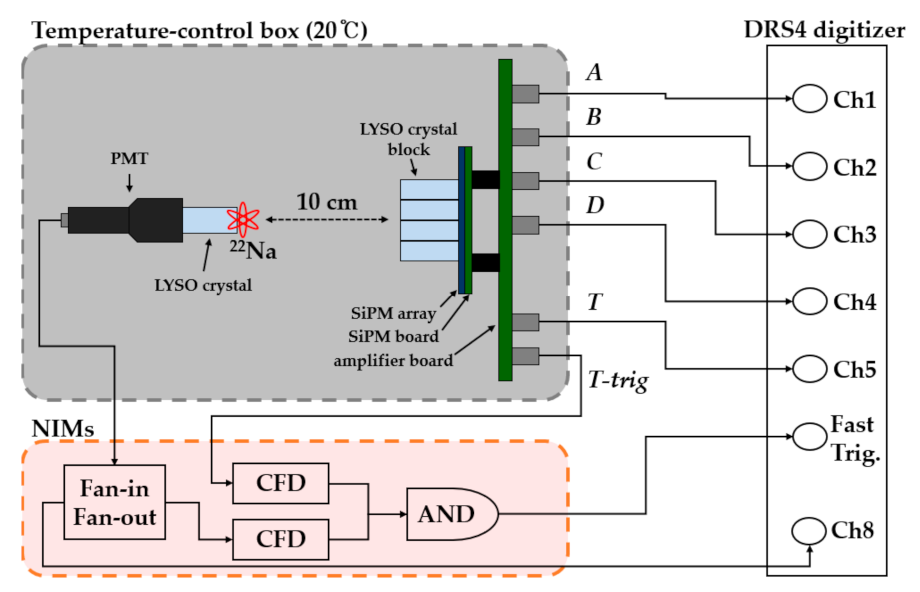
2.3. Experimental Setup

Figure 3 shows the experimental setup used in this study. All the experiments were performed at 20 °C in a temperature-controlled box. We used a reference detector based on a Hamamatsu R9800 photomultiplier tube (PMT) coupled with a single 4 × 4 × 10 mm3 LYSO crystal. The single timing resolution (STR) of the reference detector was 252 ps FWHM. A 22 Na point source (~8 μCi) was placed at the PMT entrance window. The distance between the PET detector module and the reference detector was 10 cm. We employed a series of nuclear instrumentation modules (NIMs) for coincidence detection. The PMT dynode signal was duplicated via a fan-in/fan-out NIM (N401, CAEN). Both timing signals (T-trig.) and the PMT dynode signal were fed into a NIM constant fraction discriminator (CFD) (N843, CAEN) to generate a trigger signal. The trigger signals from the PET detector module and reference detector were fed into a NIM AND logic gate (N455, CAEN) and subsequently connected to a fast-trigger port (TR0) as an input for a domino-ring sampler 4 (DRS4)-based digitizer (DT5742 B, CAEN). Each PMT dynode signal, four-corner signals, and timing signal were individually sampled by the DRS4 digitizer with a sampling rate of 5 giga samples per second (GSPS).

2.4. Data Analysis

The deposited energy of the annihilation photons was calculated by summing the integrated charge of each four-corner signal (Figure 4a). The integration window was 150 ns. The energy resolution was estimated by fitting the 511 keV photopeak window with a Gaussian curve. We generated a 2 D flood histogram using the integrated charge of each of the four-corner signals using the following equations:
x =   Q A   +   Q B     Q C     Q D Q A   +   Q B   +   Q C   +   Q D
y =   Q A     Q B     Q C   +   Q D Q A   +   Q B   +   Q C   +   Q D
where QA, QB, QC, and QD correspond to the integrated charge from each of the four-corner signals.
The arrival time of the annihilation photons was measured by applying the digital leading-edge discrimination (LED) method with a threshold of 7% of the pulse amplitude that falls into the energy window around the 511 keV photopeak. The baseline correction was performed on an event-by-event basis. Only the coincidence events that fell into the energy window of [-FWHM, FWHM] around the 511 keV photopeak were used for the CTR measurement. To avoid high-frequency noise interference between the adjacent data acquisition (DAQ) channels within the DRS4 chip, we performed an inter-chip measurement [21]. We comparatively evaluated the PET timing performance with and without applying the capacitive filtering techniques for the three different SiPM arrays (Figure 4b). We characterized the timing performance of each SiPM array with varying SiPM overvoltages ranging from 5 to 10 V.

3. Results

3.1. Flood Histogram

Figure 5 shows the 2 D flood histograms. All 16 LYSO crystal elements were clearly separated from the flood histograms. However, the resolution was degraded at the edges and corners of the scintillator array as shown in Figure 6.

3.2. Energy Performance

Figure 7 shows the photopeak value as a function of overvoltage. The photopeak value reflects the amount of visible photons collected from scintillation crystals. A similar tendency in the light output was observed for the 3 and 4 mm arrays. At an overvoltage of 5 to 7 V, the 3 and 4 mm arrays yielded a higher photopeak value than the 6 mm array. As the overvoltage increased, the photopeak value of the 6 mm array exceeded those of the 3 and 4 mm arrays, yielding the highest light output at an overvoltage of 10 V.
Figure 8 shows the energy resolution as a function of the overvoltage. The average energy resolution with application of an analog high-pass filter was 11.4% ± 0.8%, 11.1% ± 0.7%, and 10.6% ± 0.6% for the 3, 4, and 6 mm arrays, respectively. The average energy resolution without application of the analog high-pass filter was 11.1 ± 0.3%, 10.8 ± 0.4%, and 10.4 ± 0.3% for the 3, 4, and 6 mm arrays, respectively. The best energy resolution was achieved with the 6 mm array and could be attributed to the higher photopeak value, which reflects a higher photon detection efficiency owing to the 6 mm array having a larger number of microcells than the 3 and 4 mm arrays.

3.3. Timing Performance

Figure 9 shows the CTR value as a function of the overvoltage. Without application of the analog high-pass filter, the best CTR values of 733, 747, and 751 ps FWHM were achieved for the 3, 4, and 6 mm arrays, respectively. The timing performance was significantly improved by applying the analog high-pass filter with the best CTR values of 417, 430, and 401 ps FWHM for the 3, 4, and 6 mm arrays, respectively. The analog high-pass filter greatly improved the timing performance of large-area SiPM arrays by effectively reducing the baseline fluctuation induced by dark currents [19,20].

4. Discussion

The PET detector technology that has been the most actively studied in recent years is accurately measure time-of-flight [19,22,23,24,25,26,27,28], depth-of-interaction [29,30,31,32], and inter-crystal scattering [33,34,35]. PMTs traditionally used for PET detectors have the advantage of high quantum efficiency [23,36], but block detectors based on PMTs have limitations in improving the time resolution owing to light loss between the PMTs. To overcome this drawback, time-of-flight PET detectors using position-sensitive multi-anode PMTs have been proposed [24,25,26]. However, owing to the high price of position-sensitive PMTs, the commercialization of whole-body PET scanners was halted. The performance of SiPM, which was proposed as an alternative to PMTs for simultaneous PET/MRI systems [37,38,39], has been rapidly improved, now surpassing PMTs in terms of timing resolution. In particular, the compactness of SiPMs allows for the minimization of scintillation light loss between them and the time jitter of a single photon.
The timing resolution of the PET system is determined by several detector and system components, including scintillation crystals and photosensors. Precise time measurement electronics are also important components for obtaining good timing resolution of PET [27,28]. Although a SiPM has good timing properties, multiplexing many SiPMs to a single readout channel using resistive and capacitive charge division networks causes significant degradation of timing resolution. In this study, each SiPM anode signal was divided into timing and position signals, and the timing signals were multiplexed and amplified using a dual-stage non-inverting amplifier after passing through a first-order capacitive high-pass filter [19,20]. The high-pass filtering of the timing signal resulted in a significant improvement in CTR (Figure 9). The photopeak channels of annihilation photons, estimated by summing the position signals, does not seem to be affected by high-pass filtering (Figure 7).
Comparing the various detector performance indicators, the 6 mm array performed similarly to or better than the 3 and 4 mm arrays. All 3.85 × 4.3 × 20 mm3 LYSO crystals were resolved well in the flood map regardless of the SiPM array types. The energy performance was similar among the three different SiPM arrays, with an energy resolution of approximately 10–11%. The best timing performance was achieved for the 6 mm array with a CTR value of 401 ps FWHM. As the dimension of crystal block is smaller than the total photosensitive area of each SiPM array, it might affect to the performance of boundary crystals. Therefore, we plan to further evaluate each SiPM array using an LSO crystal block that perfectly matches the entire coverage of each SiPM array.
Several electronics techniques have been attempted to improve the time resolution of the PET detector. One of the technologies that has recently received attention is the capacitance compensation circuits that reduce effective device capacitance [22,40,41]. Another notable technique is improving the accuracy of time-of-flight estimation using deep learning [42], which has been successful in many medical image and signal processing fields [43,44,45,46,47]. However, these interesting techniques have so far been applied only to single-channel scintillation detectors. It will be necessary to study whether it is possible to improve the time resolution of multiplexed SiPM array-based PET detectors by applying these techniques.
Although all individual elements in scintillator arrays were resolved well in the flood histograms, the resolution was degraded at the edges and corners of the scintillator array as shown in Figure 6. In the DPC Network used for charge (current) division in this study, the output impedance of signal source should be high and the four-corner signals (i.e., A, B, C, and D outputs) should be terminated with low impedance amplifiers (e.g., charge or current sensitive amplifiers) [18]. Unideal signal source output impedance and DPC termination impedance are potential sources of the pincushion distortion and resolution degradation at the edges and corners shown in Figure 5 and Figure 6. Therefore, it will be necessary to upgrade our DPC to mitigate the degradation while maintaining good timing resolution. It needs to be modified to adopt high output capacitance SiPMs, and other analog position encoding network can also be considered.

5. Conclusions

In this study, we characterized a large-area SiPM array that features different active areas of 3 × 3, 4 × 4, and 6 × 6 mm2, respectively. We expect that the 6 mm array can provide a cost-effective solution for whole-body PET applications in combination with high-performance SiPM multiplexing. Further optimization of the timing performance will be performed to enhance the time-of-flight capability of whole-body PET applications.

Author Contributions

Conceptualization, M.S., H.P., and J.S.L.; methodology and investigation, M.S. and H.P; writing—original draft preparation, review, and editing; M.S., H.P., and J.S.L.; supervision and funding acquisition, J.S.L. All authors have read and agreed to the published version of the manuscript.

Funding

This work was supported by grants from the National Research Foundation of Korea (NRF) funded by the Korean Ministry of Science, ICT and Future Planning (grant no. NRF-2016 R1 A2 B3014645).

Conflicts of Interest

The authors declare no conflict of interest.

References

  1. Grant, A.M.; Deller, T.W.; Khalighi, M.M.; Maramraju, S.H.; Delso, G.; Levin, C.S. NEMA NU 2-2012 performance studies for the SiPM-based ToF-PET component of the GE SIGNA PET/MR system. Med. Phys. 2016, 43, 2334–2343. [Google Scholar] [CrossRef] [PubMed] [Green Version]
  2. Hong, S.J.; Kang, H.G.; Ko, G.B.; Song, I.C.; Rhee, J.-T.; Lee, J.S. SiPM-PET with a short optical fiber bundle for simultaneous PET-MR imaging. Phys. Med. Biol. 2012, 57, 3869. [Google Scholar] [CrossRef] [PubMed]
  3. Ko, G.B.; Yoon, H.S.; Kim, K.Y.; Lee, M.S.; Yang, B.Y.; Jeong, J.M.; Lee, D.S.; Song, I.C.; Kim, S.-K.; Kim, D.; et al. Simultaneous multiparametric PET/MRI with silicon photomultiplier PET and ultra-high-field MRI for small-animal imaging. J. Nucl. Med. 2016, 57, 1309–1315. [Google Scholar] [CrossRef] [PubMed] [Green Version]
  4. Kwon, S.I.; Lee, J.S.; Yoon, H.S.; Ito, M.; Ko, G.B.; Choi, J.Y.; Lee, S.-H.; Song, I.C.; Jeong, J.M.; Lee, D.S.; et al. Development of small-animal PET prototype using silicon photomultiplier (SiPM): Initial results of phantom and animal imaging studies. J. Nucl. Med. 2011, 52, 572–579. [Google Scholar] [CrossRef] [PubMed] [Green Version]
  5. Lee, M.S.; Lee, J.S. Depth-of-interaction measurement in a single-layer crystal array with a single-ended readout using digital silicon photomultiplier. Phys. Med. Biol. 2015, 60, 6495. [Google Scholar] [CrossRef] [PubMed]
  6. Rausch, I.; Ruiz, A.; Valverde-Pascual, I.; Cal-González, J.; Beyer, T.; Carrio, I. Performance evaluation of the Vereos PET/CT system according to the NEMA NU2-2012 standard. J. Nucl. Med. 2019, 60, 561–567. [Google Scholar] [CrossRef] [PubMed] [Green Version]
  7. Son, J.-W.; Kim, K.Y.; Park, J.Y.; Kim, K.; Lee, Y.-S.; Ko, G.B.; Lee, J.S. SimPET: A Preclinical PET Insert for Simultaneous PET/MR Imaging. Mol. Imaging Biol. 2020, 22, 1208–1217. [Google Scholar] [CrossRef]
  8. Van Sluis, J.; De Jong, J.; Schaar, J.; Noordzij, W.; Van Snick, P.; Dierckx, R.; Borra, R.; Willemsen, A.; Boellaard, R. Performance characteristics of the digital Biograph Vision PET/CT system. J. Nucl. Med. 2019, 60, 1031–1036. [Google Scholar] [CrossRef] [PubMed]
  9. Yoon, H.S.; Ko, G.B.; Kwon, S.I.; Lee, C.M.; Ito, M.; Song, I.C.; Lee, D.S.; Hong, S.J.; Lee, J.S. Initial results of simultaneous PET/MRI experiments with an MRI-compatible silicon photomultiplier PET scanner. J. Nucl. Med. 2012, 53, 608–614. [Google Scholar] [CrossRef] [PubMed] [Green Version]
  10. Goertzen, A.L.; Zhang, X.; McClarty, M.M.; Berg, E.J.; Liu, C.-Y.; Kozlowski, P.; Retière, F.; Ryner, L.; Sossi, V.; Stortz, G.; et al. Design and performance of a resistor multiplexing readout circuit for a SiPM detector. IEEE Trans. Nucl. Sci. 2013, 60, 1541–1549. [Google Scholar] [CrossRef]
  11. Ko, G.B.; Kim, K.Y.; Yoon, H.S.; Lee, M.S.; Son, J.-W.; Im, H.-J.; Lee, J.S. Evaluation of a silicon photomultiplier PET insert for simultaneous PET and MR imaging. Med. Phys. 2016, 43, 72–83. [Google Scholar] [CrossRef] [PubMed] [Green Version]
  12. Ko, G.B.; Lee, J.S. Single transmission-line readout method for silicon photomultiplier based time-of-flight and depth-of-interaction PET. Phys. Med. Biol. 2017, 62, 2194. [Google Scholar] [CrossRef] [PubMed]
  13. Kwon, S.I.; Lee, J.S. Signal encoding method for a time-of-flight PET detector using a silicon photomultiplier array. Nucl. Instrum. Methods A 2014, 761, 39–45. [Google Scholar] [CrossRef]
  14. Park, H.; Ko, G.B.; Lee, J.S. Hybrid charge division multiplexing method for silicon photomultiplier based PET detectors. Phys. Med. Biol. 2017, 62, 4390. [Google Scholar] [CrossRef]
  15. Won, J.Y.; Ko, G.B.; Lee, J.S. Delay grid multiplexing: Simple time-based multiplexing and readout method for silicon photomultipliers. Phys. Med. Biol. 2016, 61, 7113. [Google Scholar] [CrossRef] [PubMed] [Green Version]
  16. Yamamoto, S.; Imaizumi, M.; Watabe, T.; Watabe, H.; Kanai, Y.; Shimosegawa, E.; Hatazawa, J. Development of a Si-PM-based high-resolution PET system for small animals. Phys. Med. Biol. 2010, 55, 5817. [Google Scholar] [CrossRef]
  17. Du, J.; Yang, Y.; Bai, X.; Judenhofer, M.S.; Berg, E.; Di, K.; Buckley, S.; Jackson, C.; Cherry, S.R. Characterization of large-area SiPM array for PET applications. IEEE Trans. Nucl. Sci. 2016, 63, 8–16. [Google Scholar] [CrossRef] [PubMed] [Green Version]
  18. Siegel, S.; Silverman, R.W.; Shao, Y.; Cherry, S.R. Simple charge division readouts for imaging scintillator arrays using a multi-channel PMT. IEEE Trans. Nucl. Sci. 1996, 43, 1634–1641. [Google Scholar] [CrossRef]
  19. Bieniosek, M.; Cates, J.; Grant, A.; Levin, C. Analog filtering methods improve leading edge timing performance of multiplexed SiPMs. Phys. Med. Biol. 2016, 61, N427. [Google Scholar] [CrossRef] [PubMed] [Green Version]
  20. Park, H.; Lee, J.S. Highly multiplexed SiPM signal readout for brain-dedicated TOF-DOI PET detectors. Phys. Med. 2019, 68, 117–123. [Google Scholar] [CrossRef] [PubMed]
  21. Park, H.; Lee, S.; Ko, G.B.; Lee, J.S. Achieving reliable coincidence resolving time measurement of PET detectors using multichannel waveform digitizer based on DRS4 chip. Phys. Med. Biol. 2018, 63, 24NT02. [Google Scholar] [CrossRef] [PubMed]
  22. Cates, J.W.; Levin, C.S. Electronics method to advance the coincidence time resolution with bismuth germanate. Phys. Med. Biol. 2019, 64, 175016. [Google Scholar] [CrossRef] [PubMed]
  23. Ito, M.; Lee, J.P.; Lee, J.S. Timing performance study of new fast PMTs with LYSO for time-of-flight PET. IEEE Trans. Nucl. Sci. 2012, 60, 30–37. [Google Scholar] [CrossRef]
  24. Ko, G.B.; Lee, J.S. Performance characterization of high quantum efficiency metal package photomultiplier tubes for time-of-flight and high-resolution PET applications. Med. Phys. 2015, 42, 510–520. [Google Scholar] [CrossRef] [PubMed] [Green Version]
  25. Son, J.W.; Kim, K.Y.; Yoon, H.S.; Won, J.Y.; Ko, G.B.; Lee, M.S.; Lee, J.S. Proof-of-concept prototype time-of-flight PET system based on high-quantum-efficiency multianode PMTs. Med. Phys. 2017, 44, 5314–5324. [Google Scholar] [CrossRef] [PubMed]
  26. Son, J.-W.; Ko, G.B.; Won, J.Y.; Yoon, H.S.; Lee, J.S. Development and performance evaluation of a time-of-flight positron emission tomography detector based on a high-quantum-efficiency multi-anode photomultiplier tube. IEEE Trans. Nucl. Sci. 2016, 63, 44–51. [Google Scholar] [CrossRef]
  27. Won, J.Y.; Kwon, S.I.; Yoon, H.S.; Ko, G.B.; Son, J.-W.; Lee, J.S. Dual-phase tapped-delay-line time-to-digital converter with on-the-fly calibration implemented in 40 nm FPGA. IEEE Trans. Biomed. Circuits Syst. 2015, 10, 231–242. [Google Scholar] [CrossRef]
  28. Won, J.Y.; Lee, J.S. Time-to-digital converter using a tuned-delay line evaluated in 28-, 40-, and 45-nm FPGAs. IEEE Trans. Instrum. Meas. 2016, 65, 1678–1689. [Google Scholar] [CrossRef]
  29. Ito, M.; Hong, S.J.; Lee, J.S. Positron emission tomography (PET) detectors with depth-of-interaction (DOI) capability. Biomed. Eng. Lett. 2011, 1, 70. [Google Scholar] [CrossRef]
  30. Ito, M.; Lee, M.S.; Lee, J.S. Continuous depth-of-interaction measurement in a single-layer pixelated crystal array using a single-ended readout. Phys. Med. Biol. 2013, 58, 1269. [Google Scholar] [CrossRef] [Green Version]
  31. Kang, H.G.; Ko, G.B.; Rhee, J.T.; Kim, K.M.; Lee, J.S.; Hong, S.J. A dual-ended readout detector using a meantime method for SiPM TOF-DOI PET. IEEE Trans. Nucl. Sci. 2015, 62, 1935–1943. [Google Scholar] [CrossRef]
  32. Son, J.-W.; Lee, M.S.; Lee, J.S. A depth-of-interaction PET detector using a stair-shaped reflector arrangement and a single-ended scintillation light readout. Phys. Med. Biol. 2016, 62, 465. [Google Scholar] [CrossRef] [PubMed] [Green Version]
  33. Lee, M.S.; Kang, S.K.; Lee, J.S. Novel inter-crystal scattering event identification method for PET detectors. Phys. Med. Biol. 2018, 63, 115015. [Google Scholar] [CrossRef] [PubMed]
  34. Lee, S.; Kim, K.Y.; Lee, M.S.; Lee, J.S. Recovery of inter-detector and inter-crystal scattering in brain PET based on LSO and GAGG crystals. Phys. Med. Biol. 2020, 65, 195005. [Google Scholar] [CrossRef] [PubMed]
  35. Park, H.; Lee, J.S. SiPM signal readout for inter-crystal scatter event identification in PET detectors. Phys. Med. Biol. 2020, 65, 200510. [Google Scholar] [CrossRef] [PubMed]
  36. Lee, S.; Lee, M.S.; Won, J.Y.; Lee, J.S. Performance of a new accelerating-electrode-equipped fast-time-response PMT coupled with fast LGSO. Phys. Med. Biol. 2018, 63, 05NT3. [Google Scholar] [CrossRef] [PubMed]
  37. Hong, S.J.; Song, I.C.; Ito, M.; Kwon, S.I.; Lee, G.S.; Sim, K.-S.; Park, K.S.; Rhee, J.T.; Lee, J.S. An investigation into the use of Geiger-mode solid-state photomultipliers for simultaneous PET and MRI acquisition. IEEE Trans. Nucl. Sci. 2008, 55, 882–888. [Google Scholar] [CrossRef]
  38. Lee, J.S.; Hong, S.J. Geiger-mode avalanche photodiodes for PET/MRI. In Electronics for Radiation Detection; Iniewski, K., Ed.; CRC Press: Boca Raton, FL, USA, 2010; pp. 179–198. [Google Scholar]
  39. Roncali, E.; Cherry, S.R. Application of silicon photomultipliers to positron emission tomography. Ann. Biomed. Eng. 2011, 39, 1358–1377. [Google Scholar] [CrossRef] [PubMed] [Green Version]
  40. Kwon, I.; Kang, T.; Wells, B.T.; Lawrence, J.; Hammig, M.D. Compensation of the detector capacitance presented to charge-sensitive preamplifiers using the Miller effect. Nucl. Instrum. Method A 2015, 784, 220–225. [Google Scholar] [CrossRef]
  41. Zhang, N.; Schmand, M.J. Bootstrapping Readout for Large Terminal Capacitance Analog-SiPM Based Time-of-Flight PET Detector. U.S. Patent No. 10,128,801, 13 November 2018. [Google Scholar]
  42. Berg, E.; Cherry, S.R. Using convolutional neural networks to estimate time-of-flight from PET detector waveforms. Phys. Med. Biol. 2018, 63, 02lt1. [Google Scholar] [CrossRef] [PubMed]
  43. Hegazy, M.A.A.; Cho, M.H.; Cho, M.H.; Lee, S.Y. U-net based metal segmentation on projection domain for metal artifact reduction in dental CT. Biomed. Eng. Lett. 2019, 9, 375–385. [Google Scholar] [CrossRef] [PubMed]
  44. Hwang, D.; Kang, S.K.; Kim, K.Y.; Seo, S.; Paeng, J.C.; Lee, D.S.; Lee, J.S. Generation of PET attenuation map for whole-body time-of-flight (18)F-FDG PET/MRI using a deep neural network trained with simultaneously reconstructed activity and attenuation maps. J. Nucl. Med. 2019, 60, 1183–1189. [Google Scholar] [CrossRef] [Green Version]
  45. Park, J.; Hwang, D.; Kim, K.Y.; Kang, S.K.; Kim, Y.K.; Lee, J.S. Computed tomography super-resolution using deep convolutional neural network. Phys. Med. Biol. 2018, 63, 145011. [Google Scholar] [CrossRef] [PubMed]
  46. Shojaedini, S.V.; Beirami, M.J. Mobile sensor based human activity recognition: Distinguishing of challenging activities by applying long short-term memory deep learning modified by residual network concept. Biomed. Eng. Lett. 2020, 10, 419–430. [Google Scholar] [CrossRef] [PubMed]
  47. Lee, J.S. A review of deep learning-based approaches for attenuation correction in positron emission tomography. IEEE Trans. Radiat Plasma Med. Sci. 2021, 5, 160–184. [Google Scholar] [CrossRef]
Figure 1. Detailed schematic of amplifier board. (a) Silicon photomultipliers (SiPM) biasing and signal path as an input for discretized positioning circuit (DPC) network and timing signal, respectively. (b) Non-inverting amplifier for generating position and deposited energy information. (c) Dual-stage non-inverting amplifier for generating trigger signal.
Electronics 10 00698 g001
Figure 2. DPC network for the (a) 3 mm array, (b) 4 mm array, and (c) 6 mm array. The 6 mm array required the smallest number of electronic components, thereby achieving less complex PCB design per unit area.
Electronics 10 00698 g002
Figure 3. Experimental setup.
Electronics 10 00698 g003
Figure 4. Waveforms of the (a) four-corner signals, and (b) timing signals after amplified by non-inverting amplifier as shown in Figure 1b,c.
Electronics 10 00698 g004
Figure 5. Flood histogram for the (a) 3 mm array, (b) 4 mm array, and (c) 6 mm array.
Electronics 10 00698 g005
Figure 6. Position dependency of resolution: (a) Flood histogram for 6 mm array measured using overvoltage yielding the best timing resolution and (b) horizontal and vertical projection histograms and FWHM (pixel) of peak distributions of projection histograms.
Electronics 10 00698 g006
Figure 7. Photopeak value as a function of the overvoltage: (a) With and (b) without application of the analog high-pass filter.
Electronics 10 00698 g007
Figure 8. Average energy resolution as a function of overvoltages: (a) With and (b) without application of the analog high-pass filter.
Electronics 10 00698 g008
Figure 9. Average coincidence timing resolution (CTR) as a function of overvoltages: (a) With and (b) without application of the analog high-pass filter.
Electronics 10 00698 g009
Publisher’s Note: MDPI stays neutral with regard to jurisdictional claims in published maps and institutional affiliations.

