Abstract
This study proposes a new method to design an analog circuit based on the control model of the circuit, and the method is applied in the design of the power amplifiers for driving piezoelectric stack actuators. Focusing on the stability of the circuit, two power amplifiers for driving piezoelectric stack actuators are analyzed deeply. The power amplifier using high-voltage operational amplifiers has a simple circuit structure, and the bandwidth and the ripple of the power amplifier are about 43 kHz and 16 mV, respectively. As for the power amplifier using general operational amplifiers, it possesses the qualities of low cost and simple circuit structure, and the bandwidth and the ripple are 53 kHz and less than 2 mV, respectively. Moreover, the proposed power amplifiers can well drive the mechanism stage during the moving range of the piezoelectric stack actuator, and the travelling ranges are both about 13 μm. Viewing the circuit design as control system design, applying control system design method in circuit design and working with PSpice simulation of the circuit: these are the main contents of the proposed method, and the method offers an answer to designing a power amplifier systematically.
1. Introduction
The circuit shown in Figure 1 is very common, and it might be introduced in every textbook about circuit theory. When the operational amplifier is ideal, the voltage VOUT can be expressed as:
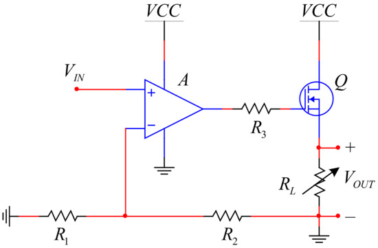
Figure 1.
Current expansion circuit for operational amplifier.
It is obvious that the ideal operational amplifier cannot be found, so that Equation (1) is an approximation. When VIN is realized by voltage references, the circuit can be considered as a voltage source. It is common that the voltage of voltage sources drops while the load resistance of the voltage sources is made smaller, but Equation (1) does not offer the information. It is valuable to explore new method to analyze such circuits deeply.
Some studies have done such work. Reference [1] proposes a new operational amplifier model for evaluating test strategies at a behavioral level, and the simulation results show that the model presents a good agreement with the transistor-level version of the amplifier. Reference [2] proposes a method to fully characterize noise in the operational amplifier; the method allows the extraction not only of the spectra of the equivalent input current noise and equivalent input voltage noise generators but also of their cross-correlation coefficients, and a key finding is that neglecting the cross-correlation coefficient between the two equivalent input current noises can lead to severe errors in noise analysis. In reference [3], a high input impedance circuit to convert a single ended voltage to its differential counterpart is proposed, and the design makes full use of the characteristics of operational amplifiers and well applies closed-loop feedback control. In reference [4], the equivalent small parameter method is used to establish the nonlinear mathematical model of the fractional-order buck–boost converter in continuous current mode, and the method has achieved satisfying results. In reference [5], a unified model is proposed for small-signal modelling in current controlled converters using the discrete-time analysis method, and simulations and experiments are committed to verify the proposed model. Reference [6] introduces an additional operational amplifier that is utilized as a buffer to improve the Howland voltage controlled current source, a complete analysis including a new two-port analysis of the circuit is presented, and the results indicate that the method increases output impedance, improves noise performance and achieves stability easily. In reference [7], the hysteresis-PI control algorithm is used in shunt active power filter design, and the effectiveness of the filter in minimizing the current harmonics has been evaluated under balanced and unbalanced nonlinear load conditions. Reference [8] goes further, the paper applies sliding-mode controller in the design of fourth-order class-D Amplifier, and experimental results reveal that the proposed controller effectively flattens the frequency response of the fourth-order amplifier and results in THD and voltage overshoot of 0.6% and 1 V respectively. The paper [9] applies cascode and Miller compensation for three-stage amplifiers to drive a pF-to-nF capacitive load, the simulation results show at least 0.88 MHz GBW is achieved under 4 pF to 1.5 nF capacitor load while the on-chip compensative capacitance is only 1.05 pF. These works have achieved brilliant results. However, as the methods of these works can only be utilized in specific circuit designs, they can hardly be applied to other fields directly.
It is more sensible to explore the philosophical thoughts of these works rather than to study their methods, and the philosophical thoughts lie in the way these papers have applied system modelling or control theory in the design of the circuit. This idea may enlighten the design of the power amplifiers for driving piezoelectric stack actuators, which are widely applied in micromachining, industrial precision positioning systems and biomedical engineering but have problems in being driven, as they always have large capacitance [10,11,12].
Some studies have done basic research. Reference [13] proposes a 15 W power amplifier to drive piezoelectric stack actuators; in order to save energy, the power supply of the high-voltage operational amplifier is controlled by the input signal, and the power amplifier has about 40 mV output voltage ripples. In reference [14], high-voltage operational amplifiers are utilized to design power amplifiers for driving piezoelectric stack actuators directly, high-voltage operational amplifiers need dissipating heat well and the output bandwidth of the proposed power amplifier can reach 20 kHz. Applying the schematic described in Figure 1, reference [15] designs a power amplifier for driving piezoelectric stack actuators; the reference does not offer much theoretical analysis, the design relies on simulation and the output voltage ripple of the designed power amplifier is less than 20 mV. Reference [16] uses an isolation amplifier and subtracting amplifier to design an innovative power amplifier; the merits of the amplifier include a wide bandwidth and high potential power, and experiments using a six-level arrangement demonstrate a 100 kHz bandwidth with ±200 V output swing for different capacitive loadings. Reference [17] designs a high-voltage operational amplifier by discrete electronic elements; a power amplifier is proposed using the operational amplifier as a noninverting amplifier, and the ripple and bandwidth are about 2 mV and 57 kHz, respectively. There are also some works about charge drivers for piezoelectric stack actuators. In reference [18], a new charge driver circuit and electrical configuration are implemented which allows commonly available piezoelectric bimorphs to be linearized; this circuit consists of four major components: a high-voltage amplifier, a differential amplifier, a piezoelectric load and a PI feedback controller, and experiments show a significant improvement of the hysteresis of the bender when compared to a typical voltage driver. Reference [19] presents a novel controller circuit to overcome the issues of low-frequency performance, long settling time, floating-load and loss of stroke, and experimental results show that the presented charge controller can effectively reduce more than 88% of the hysteretic nonlinearity even when the operating closes to the transition frequency. These works in the mentioned references are innovative, and they all fully explore the advantages of the operational amplifier which are high input impedance and high magnification. Based on these researches and the idea applying control theory in circuit design, it is liable to propose a unified method to design power amplifiers for driving piezoelectric stack actuators, and the method is simple and flexible to be applied in engineering.
A new perspective to view the analog design is thoroughly described in this paper. The perspective creates the model of the designed circuit and analyses the essential performances by classical control theory. Based on the method, two kinds of power amplifiers for driving piezoelectric stack actuators are proposed, one uses high-voltage operational amplifiers as the controller, and the other applies general operational amplifiers. The two kinds of power amplifiers are analyzed by the proposed method which focuses on the stability of the circuit, and prototype circuit of the proposed power amplifiers is simulated and tested. Aiming to evaluate the designed power amplifiers, the power amplifiers are used to drive a 1 dimension stage during the motion range of the mechanism. Those works prove that the proposed method is a systematic approach to the design of power amplifiers and make the design of the power amplifier simple. The novelty of the paper is that the control model of the circuit is set up by the classical control theory, the performances of the circuit are analyzed by the control model qualitatively and the control model of the circuit is used to adjust the structure of the circuit and provide direction for simulation.
The organization of this paper is as follows. Section 2 presents the method based on the problem described in the introduction. In Section 3, a power amplifier using high-voltage operational amplifiers is designed, analyzed, simulated and tested. In Section 4, considering the high price and little choice of high-voltage operational amplifiers, a power amplifier using general operational amplifiers is designed, analyzed, simulated and tested. In Section 5, the designed two power amplifiers are tested with the mechanism. Finally, the main conclusions are described in Section 6.
2. The Proposed Approach
Operational amplifiers generally have outstanding amplified ability on differential-mode signals, their inputs have higher input impedance and they have excellent ability to suppress common mode signals. Therefore, their control block diagram can be shown in Figure 2. In reference [1], the transfer function A(s) can be expressed as:
where S1 and S2 are poles of the operational amplifier and A is the open loop voltage gain. Based on this characteristic of the operational amplifier, the operational amplifier can be used as the controller of the circuit and the classical feedback control theory can be applied in the analog circuit design. The schematic and the control block diagram of the analog circuit can be shown in Figure 3 and Figure 4, respectively.
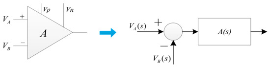
Figure 2.
The control block diagram of an operational amplifier.
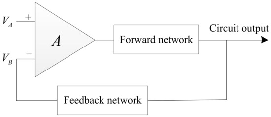
Figure 3.
The schematic of the analog circuit.
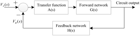
Figure 4.
The control block diagram of the analog circuit.
In the figures, G(s) is the transfer function of the forward network and H(s) is the transfer function of the feedback network. The forward network can use inner-loop feedback control to further weaken the nonlinearity of the circuit model, which makes the setting of the system easier. There are some methods to realize the inner-loop control, and the common and sensible method is utilizing the characteristics of electronic components. In the introduction, it is such an example that applies the MOSFET as the output stage of the circuit, and the circuit principle and the control block diagram of the MOSFET are shown in the Figure 5.
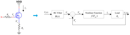
Figure 5.
The control block diagram of the MOSFET.
In the control block diagram, B(s) is the RC filter composed by Rg and the input capacitor of the gate of the MOSFET. The relationship between Id and V is generally a nonlinear function, and the voltage V is the voltage difference between Vg and Vs. The local linearization of the function can be expressed by Equation (3):
where V0 is the bias voltage. The Equation (3) can be further expressed by Equation (4):
Based on Equation (4), the model of the MOSFET can be expressed by Figure 6. In the model, K is the mutual conductance parameter of the MOSFET, which can be obtained from the manual of the MOSFET, and the parameter P can be abstracted as a disturbance.
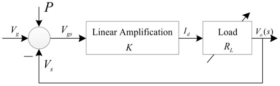
Figure 6.
The control block diagram of the MOSFET.
Based on the models of the MOSFET and the operational amplifier, the control block diagram of the circuit mentioned in the introduction can be expressed as Figure 7.
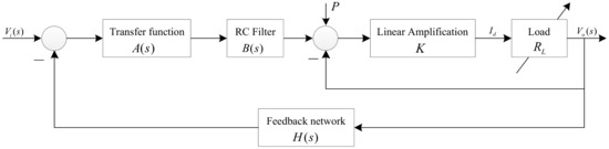
Figure 7.
The control block diagram of the circuit mentioned in the introduction.
Based on the control block diagram, the transfer function of the system can be described as:
In Equation (5), the parameter K1 can be expressed by Equation (6):
where RL is the resistance value of the load. Based on the control block diagram shown in Figure 7, the load regulation rate of the voltage source in the introduction is caused by the steady-state error of the control system as the load RL is changed. In order to reduce the steady-state error, it is liable to increase the open-loop gain of the whole system as much as possible when the system is stable.
The proposed method, exploiting the characteristics of the operational amplifier and some electronic components, transforms the design of the analog circuit into the design and calibration of the control systems, and the method can be effectively applied in the design of power amplifiers for driving piezoelectric stack actuators.
3. Power Amplifiers Using High-Voltage Operational Amplifiers
3.1. The Model of the Power Amplifier and Its Stability Analysis
The schematic of the power amplifier using high-voltage operational amplifiers is shown in Figure 8. Based on the circuit mentioned in the introduction, to the circuit is added a negative current output circuit and PA341DF is selected as the operational amplifier. The power supplies VCC and VSS are 130 V and −15 V, respectively. The control block diagram of the circuit is shown in Figure 9. As introduced in Section 2, the high-voltage operational amplifier forms the subtracter and the controller A(s), the resistance R1 or R2 and the input capacitance of the next stage form the filter D(s), the load is the capacitor which replaces the piezoelectric stack actuator and the MOSFETs are modelled as the inner feedback control loop. R4-5 and C2 are modelled as the feedback network of the circuit, whose transfer function is H(s).
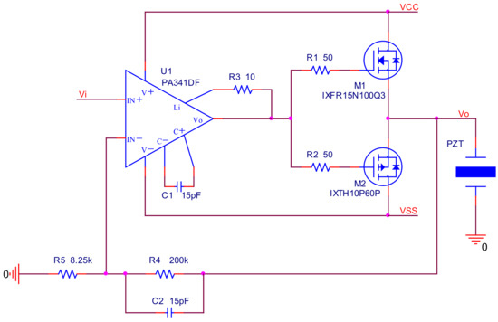
Figure 8.
The schematic of the power amplifier using high-voltage amplifiers.
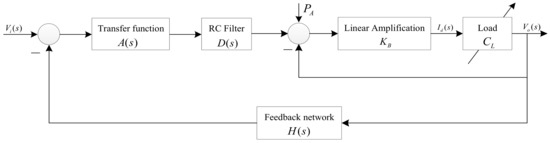
Figure 9.
The control block diagram of the circuit.
The parameters of the models can be found in the manuals of the electronic components; some values of those electronic components are changed during a range, but the closed-loop control system can effectively reduce the influence of the parameters’ dispersion on the final control results. The parameters are shown in Table 1.

Table 1.
The parameters of the control block diagram.
The parameter KB is taking from the conductance parameter of NMOSFET M1, and the range can be determined as 0.5–100 based on the manual of the device. The range is large, which completely covers the changing range of conductivity parameter and fully considers the change of open-loop gain. Based on the control block diagram, the transfer function of the power amplifier is described as:
where X(s) is the transfer function of the inner loop. As the control system model of the circuit has been established, the analysis of the control system is different for different circuits. As to the power amplifiers, the most important analysis is the stability of the control system. While the open-loop gain of the circuit is changed from 0.5 to 100, the root locus of the circuit is shown in Figure 10, and the figure has given the changes as the open-loop gain becomes larger.
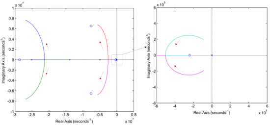
Figure 10.
The root locus of the power amplifier.
The root locus is the path of the roots of the characteristic equation traced out in the s-plane as a system parameter is changed, which is the open-loop gain in the design. Analyzing the root locus of the circuit, the roots of the closed loop control system always have negative real parts as the open-loop of the circuit changes, so that the conclusion can be draw that the circuit is stable as the open-loop gain is changed in its range. When the value of the open-loop gain is determined, the performances of the circuit can be calculated by the transfer function of the closed-loop control system. As the value KB cannot be directly gotten from the manual, the concrete value of the open-loop gain is always difficult to be obtained. So it is more convenient to simulate the circuit by PSpice when the circuit is convinced to be stable.
3.2. Simulation and Analysis
Software Cadence 16.6 is a powerful tool to simulate the analog circuit, and it is used to implement the simulation of the power amplifier. In the simulation, the positive and negative powers are set as +130 V and −15 V, respectively.
Figure 11 presents the simulated amplitude–frequency characteristic of the power amplifier. It is easy to achieve the conclusions that the passband magnification is 28.04 dB, and the system bandwidth and the 0 dB bandwidth are about 42 kHz and 1.7 MHz, respectively. In analog circuit analysis, the magnification is determined by H(s) during the low frequency range, the value is 25.24 times (about 28.04 dB) and the simulation results are in line with this principle.
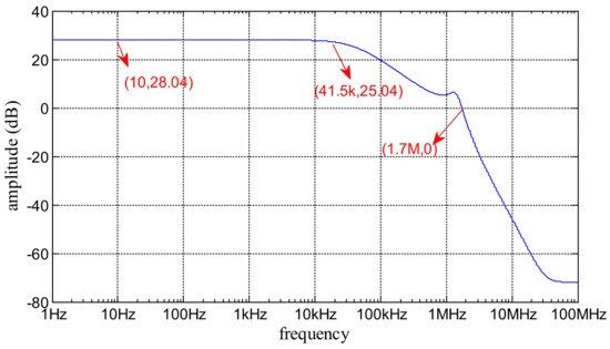
Figure 11.
Simulated amplitude-frequency characteristic of the power amplifier using the high-voltage operational amplifier.
The responses of the designed power amplifier to periodic signals such as a sinusoidal wave and square wave are important ways to value the circuit performances. Connecting the input to a sinusoidal wave which has 5 V amplitude, 2.5 V offset and 100 Hz frequency, the simulated input–output waveforms are described in Figure 12. When connecting the input to a square wave which has 5 V amplitude, 100 Hz frequency and 10 µs rising and failing time, the simulated input–output waveforms are described in Figure 13, which contains the details of the rising edge and falling edge. According to Figure 11, Figure 12 and Figure 13 the input signals are well amplified by the power amplifier and the output signals have on obvious distortion. The transient response agrees with the amplitude–frequency characteristic of the power amplifier. The reason for setting the frequency of the periodic at 100 Hz is that the motion frequency of the mechanism which the power amplifier is applied in is lower than 100 Hz.
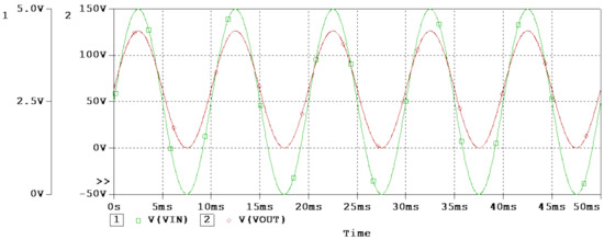
Figure 12.
Simulated sinusoidal input–output response for the power amplifier using high-voltage operational amplifiers.
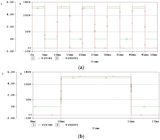
Figure 13.
Simulated square wave input–output response for the power amplifier using high-voltage operational amplifiers; (a) the overall perspective waveform; (b) the rising edge and the falling edge of the waveforms.
The simulated results are achieved by the PSpice circuit model, and the model has concrete values for the parameters which are uncertain in theoretical analysis. The amplitude–frequency characteristic and the transient response achieved by simulation show that the designed power amplifier has the same properties as a closed-loop control system, which is in line with the theoretical analysis.
3.3. Experimental Results and Comments
The tests to evaluate the power amplifier are described in Figure 14. The power supplies are two DH1722A-5s from Dahua Radio Instrument Factory [20], and the voltage powers are set as −15 V and 130 V, respectively. The waveform generator producing the desired signal is 33622B from Keysight Technologies [21], the tests use an oscilloscope (MSO5204, Tektronix Corporation [22]) to achieve the waveforms and the amplitude–frequency characteristic of the power amplifier is achieved by a network analyzer (E5061B, Keysight Technologies [21]). The test uses a high-voltage capacitor (250 V, 4.7 μF) as the load of the designed power amplifier.
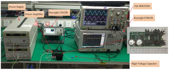
Figure 14.
The tests for the power amplifier using high-voltage operational amplifiers.
Figure 15 presents the frequency–amplitude characteristic of the designed power amplifier. In the figure, the magnification of the passband is 28.043 dB, the system bandwidth is about 43 kHz and bandwidth for 0 dB is about 2.19 MHz. Compared with the simulated result, the overall shape of the measured frequency–amplitude characteristics agrees with the results of simulation analysis during the range from DC to 0 dB bandwidth; the simulation result is different from the measured result, as the frequency is higher than 10 MHz; but the differences would have few impacts on the application of the power amplifier. When the frequency is higher than several MHz, the parameter of the print circuit board and the distribution parameters of the electronic components could not be neglected simply. The power amplifier works mainly during the passband whose frequency is always less than several kHz, and the differences between the measured frequency and the simulated frequency at the key frequency points are tiny; it is sensible to consider that the results of the measurement are in line with the results of the simulation.
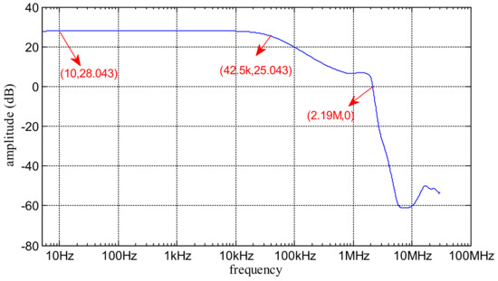
Figure 15.
Measured frequency–amplitude characteristic for the power amplifier using high-voltage operational amplifier.
The output ripple is an important performance to evaluate the circuit noise in the time domain, and it is common to use oscilloscopes to measure the circuit ripple as the input terminate of the circuit is connected to the ground. As the output displacement accuracy of the piezoelectric stack actuator is influenced by the output ripple of power amplifiers, the output ripple is a critical performance for power amplifiers. When measuring the output ripple of the designed power amplifier, a probe (P2221 from Tektronix Corporation [22]) was used as the probe in order to limit the input frequency to 6 MHz. Figure 16 shows the achieved ripple of the power amplifier, and it is considered that the output ripple of the power amplifier is less than 16 mV.
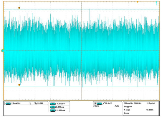
Figure 16.
Measured ripple of the power amplifier using high-voltage operational amplifier.
When testing the power amplifier, as the input signal is periodic, a high-voltage capacitor (250 V, 4.7 μF) is used as the load of the power amplifier. Using the waveform generator to produce a 100 Hz sinusoidal wave or 100 Hz square wave as the input of the power amplifier, respectively, the parameters of these waves agree with the simulation, and the measured input–output waveforms are demonstrated in Figure 17 and Figure 18. Analyzing the output signal, the conclusion can be draw that the power amplifier can respond to the periodic input well, and it agrees with the simulation results.
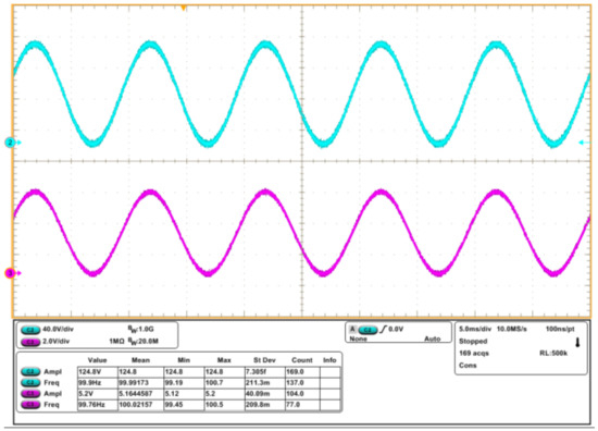
Figure 17.
Measured sinusoidal input–output waveforms for the power amplifier using high-voltage operational amplifiers.
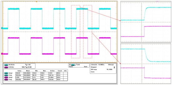
Figure 18.
Measured square wave input–output waveforms for the power amplifier using high-voltage operational.
The measured results show that the proposed design method can be applied in the design of power amplifiers flexibly. The designed power amplifier has good performances, and it can be used to drive piezoelectric stack actuators. Furthermore, based on the circuit structure shown in Figure 8, a series of power amplifiers can be designed and analyzed by the proposed method.
4. Power Amplifiers Using General Operational Amplifiers
4.1. The Model of the Power Amplifier and Its Stability Analysis
High-voltage operational amplifiers are more expensive than general operational amplifiers, and it is meaningful to apply general operational amplifiers to design power amplifiers for driving piezoelectric stack actuators. Based on the proposed method, the schematic and the control block diagram of the designed power amplifier are shown in Figure 19 and Figure 20. Just as shown in the figures, the operational amplifier OPA228U is selected, and it forms the subtracter and the controller A(s). The resistance R5 and the input capacitance of J1 form the filter D(s), and the feedback network is realized by R9-10 and C2 whose transfer function is H(s). The amplification of voltage and current is realized by the transistor circuit, and the transfer function of the circuit is X(s). The transfer function X(s) can be decomposed into many functional parts. Transistors J1, Q1–3, resistors R1–2, R4 and R7 realize the voltage amplification for the circuit, and the linearized amplification can be expressed as KA. The resistance R3 or R6 and the input capacitance of the next stage form the filter B(s). Just like the power amplifier designed by the high-voltage operational amplifiers, the MOSFET is modelled as the inner feedback control loop, and the load is the capacitor CL which replaces the piezoelectric stack actuators. The circuit uses a feedback network for correction, the feedback network is realized by R8 and C1 and the transfer function is HA(s).
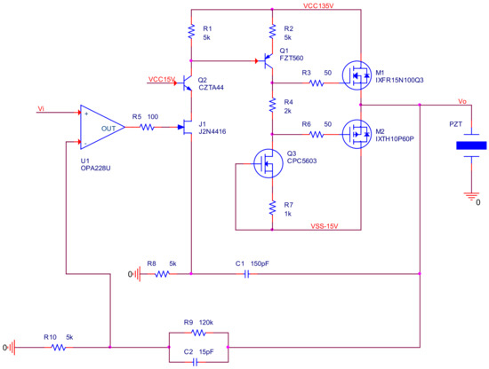
Figure 19.
The schematic of the power amplifier using general operational amplifiers.
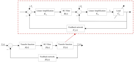
Figure 20.
The control block diagram of the power amplifier using general operational amplifiers.
The inner loop realized by MOSFET can reduce the impact of load CL. The transfer function X(s) is:
where M(s) is a function of the inner loop realized by MOSFET. The simplification of Equation (8) is considered such that the amplifier realized by the transistors generally has a high magnification. In the equation, HA(s) can be expressed as:
The circuit parameters of the models in Figure 20 can be found in the manuals of the electric components. The parameters are shown in Table 2.
Table 2.
The parameters of the control block diagram.
Based on the information in Table 2, the overall transfer function can be expressed as:
The power amplifier for driving piezoelectric stack actuators needs the ability to drive a large capacitor, and the stability of the system is the most important concern in system analysis. Considering that the open-loop gain of the system would be changed 0.5–1.5 times, the change is introduced by the dispersion of circuit parameter, and the root locus of the system is shown in Figure 21.
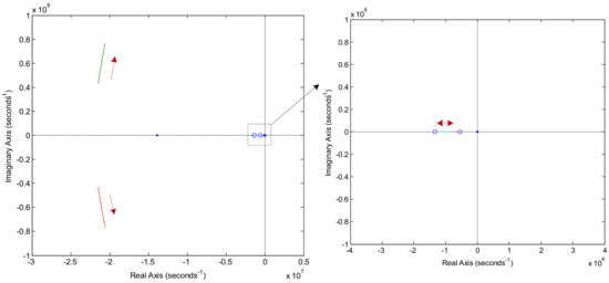
Figure 21.
The root locus of the power amplifier.
Analyzing the root locus of the circuit, the roots of the closed loop control system always have negative real parts as the gain of the circuit changes, so that the conclusion can be drawn that the circuit is stable as the open-loop gain is variable in its range. As qualitative analysis has been obtained by the control model of the circuit, the more concrete performance of the power amplifier can achieved by PSpice simulation. The control system of the circuit is modelled to draw definite conclusions and the concrete performance of the circuit is achieved by simulation: these are the essences of the proposed design method.
4.2. The Simulated and Experimental Results
As with the power amplifier using a high-voltage operational amplifier, software Cadence 16.6 is used to simulate the circuit. When implementing the simulation, the powers of VCC and VSS are set as +130 V and −15 V, respectively, and the power supplies of the operational amplifier are set as +15 V and –15 V, respectively. Figure 22 describe the test setup of the power amplifier, and the power supplies are DH1722A-5 and DH1715A-5 from Dahua Radio Instrument Factory [20] which is different from the tests of the power amplifier using high-voltage operational amplifiers.
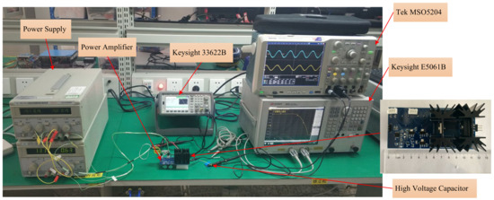
Figure 22.
Photograph of tests for the power amplifier using general operational amplifiers.
The simulated and the measured amplitude–frequency characteristics of the power amplifier are shown in Figure 23 and Figure 24. The simulated and measured magnifications are 27.96 dB and 28 dB, the simulated and measured system bandwidths are about 50 kHz and 53 kHz, and the simulated and measured 0 dB bandwidths are 847 kHz and 846 kHz, respectively. The shapes of the simulated and measured amplitude–frequency characteristics matches each other well during the range from DC to 0 dB bandwidth, and they are ideal shapes for closed-loop control system. The shapes are different, though, in the high frequency range that is about 10 MHz, and the reasons for the differences have been given in Section 3.3. Fortunately, the power amplifier works mainly during the passband whose frequency is always less than several kHz, and the differences would have few impacts on the application of the power amplifier. According to the simulated and measured data, the magnification of the power amplifier can be calculated by H(s) during the low frequency range, and it is also in line with the proposed theory.
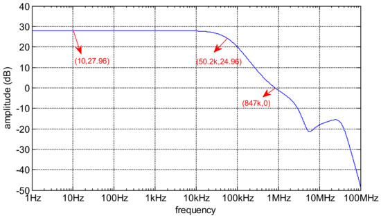
Figure 23.
Simulated frequency–amplitude characteristic for the power amplifier using general operational amplifiers.
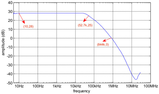
Figure 24.
Measured frequency–amplitude characteristic for the power amplifier using general operational amplifiers.
Just as with the designed power amplifier using high-voltage operational amplifiers, the simulated and measured waveforms with the input as a sinusoidal wave are shown in Figure 25 and Figure 26. In the simulation and the test, the input sinusoidal wave has 5 V amplitude, 100 Hz frequency and 2.5 V offset; while changing the input wave to a square wave whose amplitude is 5 V, frequency is 100 Hz, offset is 2.5 V and rising and failing time is 10 µs, the simulated and measured waveforms are shown in Figure 27 and Figure 28. These figures contain the rising and failing details of the waveforms, and the simulated results and the measured results match well. According to these figures, the conclusion can be draw that the designed power amplifier using a general operational amplifier can well respond to periodic input signals.
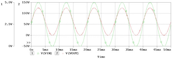
Figure 25.
Simulated waveforms for the power amplifier using general operational amplifiers.
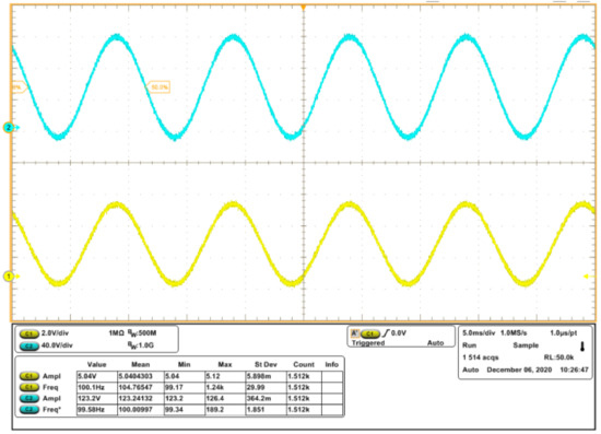
Figure 26.
Measured sinusoidal input–output waveforms for the power amplifier using general operational amplifiers.
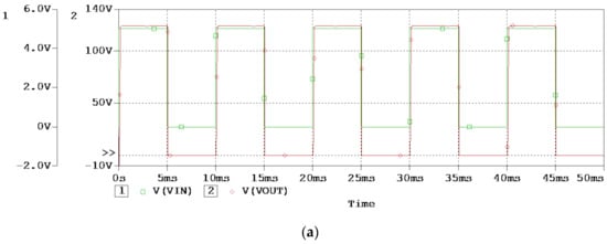
Figure 27.
Simulated waveforms for the power amplifier using general operational amplifiers; (a) the overall perspective waveform; (b) the rising edge and the falling edge of the waveforms.
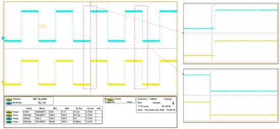
Figure 28.
Measured square wave input–output waveforms for the power amplifier using general operational amplifiers.
Just as with the designed power amplifier using high-voltage operational amplifiers, the ripple of the power amplifier using general operational amplifiers is tested while the input is connected to the ground, and the test is used to evaluate the output noise of the power amplifier. The measured ripple is shown in Figure 29, and the ripple of the designed power amplifier using general operational amplifiers is less than 2 mV. It is known that the noise of power amplifiers is decided by the first stage of the power amplifiers, and general operational amplifiers have a better performance on noise than high-voltage operational amplifiers, so that the ripple of the power amplifiers using general operational amplifiers is lower than the power amplifier using high-voltage operational amplifiers.
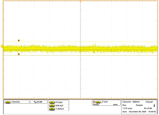
Figure 29.
Measured ripple of the power amplifier using general operational amplifiers.
The simulated and measured results of the power amplifier are presented by comparison, and the two results match each other well. The simulation and the tests demonstrate that the proposed method could well be applied in the design of the power amplifier.
5. Tests with Mechanical Stage and Some Comparisons
The tests with the mechanical stage are shown in Figure 30. The mechanical stage is driven by a piezoelectric stack actuator, whose type and producer are P887.51 and Physik Instrumente [23], respectively, and the maximum displacement of the mechanical stage of 1 degree of freedom is about 13 μm. A grating ruler (Heidenhain LIP281) installed in the mechanical stage can measure the displacement of the mechanical stage, and the displacement can be acquired and stored by the grating ruler acquisition circuit. The designed two power amplifiers are used to drive the piezoelectric stack actuator, respectively, and the input signal of the power amplifiers is generated by a waveform generator (Keysight 33622B). The tests are done in a constant temperature laboratory, and the laboratory is controlled by a precise environmental control system whose ambient temperature is 22 ± 0.2 °C.
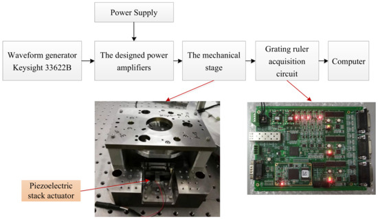
Figure 30.
The tests with the mechanical stage.
The input signal is shown in Figure 31, and the step voltage and the step time of the input signal are 0.4 V and 10 ms, respectively. The displacements of the mechanical stage excited by the designed two power amplifiers are shown in Figure 32. According to these figures, the output displacements of the mechanical stage driven by the proposed two power amplifiers are both about 13 μm, and the positive and negative steps of the displacement are both about 1.3 μm. The data demonstrate that the proposed two power amplifiers can drive the piezoelectric stack actuator well. Although the designed two power amplifiers have different electronic performances on ripples and bandwidth, there are few differences on the mechanical performances between the designed two power amplifiers.
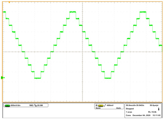
Figure 31.
The input voltage signal generated by the waveform generator.
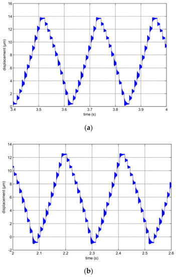
Figure 32.
The output displacements of the mechanical stage: (a) the output displacement exited by the power amplifier using high-voltage operational amplifiers; (b) the output displacement exited by the power amplifier using general operational amplifiers.
The comparisons between the power amplifiers proposed in this paper and some references are listed in Table 3. The main performances of the power amplifiers listed in the table are ripple, bandwidth, cost, size and circuit complexity. The circuit complexity of power amplifiers is evaluated by the structure of power amplifiers and the number of electric elements used in the circuit. The designed power amplifiers in this paper using high-voltage operational amplifiers and general operational amplifiers are referenced as work A and work B, respectively. Considering the power amplifiers in reference [14], reference [15] and the work A, they all reduce the circuit complexity by the integrated device (high-voltage operational amplifiers), which makes the price higher. The power amplifier B possesses the qualities of low ripple, small size, low cost and simple circuit structure, which reveals the superiority of the proposed method.
Table 3.
Comparisons between the power amplifiers proposed in this paper and some references.
6. Conclusions
In this article, a new method to design analog circuits is introduced in detail. The method views the circuit as a closed-loop feedback control system, sets up the control model of the designed circuit, uses operational amplifiers as controller of the control system and applies the correction method of classical control theory to adjust the structure and parameters of the circuit. Based on the control model of the circuit, the method can analyze the crucial performance of the circuit, which is stability in the design of power amplifiers, and offers orientation for circuit simulation and circuit parameter adjusting. Applying the proposed method in the design of power amplifiers which are applied to drive a piezoelectric stack actuator, two power amplifiers using different kinds of operational amplifiers are designed. The designed two power amplifiers can well respond to the periodic input; the system bandwidths of designed two power amplifiers are about 43 kHz and 53 kHz; the ripples of the designed two power amplifiers are less than 16 mV and 2 mV; and the designed two power amplifiers can stably drive the mechanical stage during its motion range. The successful application of the method to design power amplifiers has shown that the proposed method is simple, that the method can be realized in engineering easily, and that it could be widely applied in the design of power amplifiers.
Author Contributions
L.X., methodology, investigation, experiment data analysis and writing—original draft, review and editing; H.L., supervision and funding acquisition; P.L., conceptualization; C.G., conceptualization. All authors have read and agreed to the published version of the manuscript.
Funding
This research was funded in part by the National Science and Technology Major Project of China (Grant No. 2009ZX02205).
Conflicts of Interest
The authors declare that they have no conflict of interest in this work.
References
- Romero, E.; Peretti, G.; Marqués, C. An operational amplifier model for evaluating test strategies at behavioural level. Microelectron. J. 2007, 38, 1082–1094. [Google Scholar] [CrossRef]
- Giusi, G.; Crupi, F.; Pace, C.; Magnone, P. Full Model and Characterization of Noise in Operational Amplifier. IEEE Trans. Circuits Syst. I Regul. Pap. 2009, 56, 97–102. [Google Scholar] [CrossRef]
- Spinelli, E.M.; Haberman, M.A.; Guerrero, F.N.; García, P.A. A High Input Impedance Single-Ended Input to Balanced Differential Output Amplifier. IEEE Trans. Instrum. Meas. 2020, 69, 1682–1689. [Google Scholar] [CrossRef]
- Fang, S.; Wang, X. Modeling and analysis method of fractional-order buck–boost converter. Int. J. Circuit Theory Appl. 2020, 48, 1493–1510. [Google Scholar] [CrossRef]
- Xu, S.; Wang, C.; Lu, S.; Sun, W. Small-signal modelling for time-length compensation algorithm in current controlled converters. Int. J. Circuit Theory Appl. 2020, 48, 148–155. [Google Scholar] [CrossRef]
- Maundy, B.J.; Elwakil, A.S.; Gift, S.J. Enhancing the improved Howland circuit. Int. J. Circuit Theory Appl. 2019, 47, 532–541. [Google Scholar] [CrossRef]
- Imam, A.A.; Sreerama Kumar, R.; Al-Turki, Y.A. Modeling and Simulation of a PI Controlled Shunt Active Power Filter for Power Quality Enhancement Based on P-Q Theory. Electronics 2020, 9, 637. [Google Scholar] [CrossRef]
- Zaman, H.; Zheng, X.; Wu, X.; Khan, S.; Ali, H. A Fixed-Frequency Sliding-Mode Controller for Fourth-Order Class-D Amplifier. Electronics 2018, 7, 261. [Google Scholar] [CrossRef]
- Cheng, Q.; Li, W.; Tang, X.; Guo, J. Design and Analysis of Three-Stage Amplifier for Driving pF-to-nF Capacitive Load Based on Local Q-Factor Control and Cascode Miller Compensation Techniques. Electronics 2019, 8, 572. [Google Scholar] [CrossRef]
- Shao, Y.; Xu, M.; Shao, S.; Song, S. Effective dynamical model for piezoelectric stick-slip actuators in bi-directional motion. Mech. Syst. Signal Process. 2020, 145, 106964. [Google Scholar] [CrossRef]
- Deng, J.; Chen, W.; Li, K.; Wang, L.; Liu, Y. A sandwich piezoelectric actuator with long stroke and nanometer resolution by the hybrid of two actuation modes. Sens. Actuators A Phys. 2019, 296, 121–131. [Google Scholar] [CrossRef]
- Xu, Z.; Huang, H.; Dong, J. A stick-slip piezoelectric actuator with measurable contact force. Mech. Syst. Signal Process. 2020, 144, 106881. [Google Scholar] [CrossRef]
- Lin, C.Y.; Tampubolon, M.; Lo, Y.K.; Lin, J.Y.; Wu, Y.C.; Chiu, H.J. Study and implementation of a 15-W driver for piezoelectric actuators. Int. J. Circuit Theory Appl. 2017, 45, 439–454. [Google Scholar] [CrossRef]
- Milecki, A.; Regulski, R. Investigations of electronic amplifiers supplying a piezobimorph actuator. Mech. Syst. Signal Process. 2016, 78, 43–54. [Google Scholar] [CrossRef]
- Wang, D.H.; Zhu, W.; Yang, Q. A High-voltage and High-power Amplifier for Driving Piezoelectric Stack Actuators. J. Intell. Mater. Syst. Struct. 2009, 20, 1987–2001. [Google Scholar] [CrossRef]
- Tung, Y.C.; Jeng, S.L.; Chieng, W.H. Multi-level balanced isolated floating difference amplifier. IEEE Trans. Ind. Electron. Circuits Syst. I Regul. Pap. 2008, 55, 3016–3022. [Google Scholar] [CrossRef][Green Version]
- Xu, L.; Li, H.; Li, P.; Ge, C. A High-Voltage and Low-Noise Power Amplifier for Driving Piezoelectric Stack Actuators. Sensors 2020, 20, 6528. [Google Scholar] [CrossRef] [PubMed]
- Rios, S.A.; Fleming, A.J. Design of a Charge Drive for Reducing Hysteresis in a Piezoelectric Bimorph Actuator. IEEE/Asme Trans. Mechatron. 2016, 21, 51–54. [Google Scholar] [CrossRef]
- Yang, C.; Li, C.; Xia, F.; Zhu, Y.; Zhao, J.; Youcef-Toumi, K. Charge Controller with Decoupled and Self-Compensating Configurations for Linear Operation of Piezoelectric Actuators in a Wide Bandwidth. IEEE Trans. Ind. Electron. 2019, 66, 5392–5402. [Google Scholar] [CrossRef]
- Dahua Radio Instrument Factory. Available online: http://www.dhelec.com.cn/ (accessed on 23 January 2021).
- Keysight Technologies. Available online: https://www.keysight.com (accessed on 23 January 2020).
- Tektronix Corporation. Available online: https://www.tek.com.cn (accessed on 23 January 2020).
- Physik Instrumente. Available online: www.physikinstrumente.com (accessed on 23 January 2020).


Publisher’s Note: MDPI stays neutral with regard to jurisdictional claims in published maps and institutional affiliations. |
© 2021 by the authors. Licensee MDPI, Basel, Switzerland. This article is an open access article distributed under the terms and conditions of the Creative Commons Attribution (CC BY) license (http://creativecommons.org/licenses/by/4.0/).