Article

An Ultra-Low-Power K-Band 22.2 GHz-to-26.9 GHz Current-Reuse VCO Using Dynamic Back-Gate-Biasing Technique

College of Electronic and Information, Shenzhen University, Shenzhen 518060, China
*
Author to whom correspondence should be addressed.
Electronics 2021, 10(8), 889; https://doi.org/10.3390/electronics10080889
Submission received: 26 January 2021 / Revised: 1 April 2021 / Accepted: 6 April 2021 / Published: 8 April 2021
(This article belongs to the Special Issue RF/Mm-Wave Circuits Design and Applications)

Abstract

:
An ultra-low-power K-band LC-VCO (voltage-controlled oscillator) with a wide tuning range is proposed in this paper. Based on the current-reuse topology, a dynamic back-gate-biasing technique is utilized to reduce power consumption and increase tuning range. With this technique, small dimension cross-coupled pairs are allowed, reducing parasitic capacitors and power consumption. Implemented in SMIC 55 nm 1P7M CMOS process, the proposed VCO achieves a frequency tuning range of 19.1% from 22.2 GHz to 26.9 GHz, consuming only 1.9 mW–2.1 mW from 1.2 V supply and occupying a core area of 0.043 mm2. The phase noise ranges from −107.1 dBC/HZ to −101.9 dBc/Hz at 1 MHz offset over the whole tuning range, while the total harmonic distortion (THD) and output power achieve −40.6 dB and −2.9 dBm, respectively.

1. Introduction

To demand the high data rate of a wireless communication system, millimeter wave (mm-wave) is the most promising candidate due to its wide available bandwidth [1]. It is a very challenging task to design a voltage-controlled oscillator (VCO) with low power consumption, low phase noise and wide tuning range, which are limited by each other. Nowadays, handheld devices are rapidly increasing and circuits with low power dissipation are critical. VCOs occupy most power consumption in PLLs, of which more than half comes from oscillators. Recently, VCOs have evolved from a single LC-tank (e.g., class-B [2] and class-C [3]) to the multi-resonant tank (e.g., class-F) [4,5,6]. In order to tackle the power consumption challenge, current-reuse topology has become more and more popular. The authors in [7] first demonstrated NMOS–PMOS cross-coupled pairs to form current-reuse topology. Compared with conventional structure, negative pairs are switched on or switched off simultaneously, reducing half of the power consumption. Based on [7], several topologies are developed, such as [4,5]. Although this topology can achieve excellent phase noise performance and a wide tuning range, the design of transformers is difficult and complicated. The authors in [8,9] proposed a transformer feedback technique to realize low power consumption with low phase noise. The authors in [10] achieved low power with Colpitts VCO and proposed the Gm-Boosting technique and forward-body self-biased technique to reduce power consumption. However, the phase noise performance of this structure is not so good. In addition, two capacitors are needed to divide the resonant cavity and the transistor, resulting in more die area. At the same time, multi-core VCOs are an area of focus in mm-wave [11,12] which can achieve a wide tuning range and a low phase noise but with the cost of complicated design flow, power consumption and die area. Therefore, single-core VCO remains the most popular topology.
Based on the current-reuse topology [7], a more effective and simple method was proposed in this paper to achieve low power and wide tuning range simultaneously. The method relies on the dynamic back-gate-biasing technique, which periodically adjusts cross-coupled pairs’ bulk to change threshold voltage in different status. At the same time, the technique can relax start-up condition with direct voltage in cross-couple pairs, so smaller dimension negative cross-coupled pairs are allowed, which can significantly reduce power dissipation and parasitic capacitance. This technique uses the asymmetry of the output in current-reuse topology, so an error voltage can be extracted from inductance with central tap and fed back to bulk. In mm-wave VCOs, parasitic capacitance is a serious problem and small dimension transistors are necessary. The detailed principle will be discussed in the next section.
The paper is organized as follows: Section 2 introduces the proposed topology and its simplified small signal model. Additionally, the relevant design principle is discussed. Section 3 demonstrates the post-layout simulation results, and Section 4 draws a conclusion.

2. Design and Analysis of CR_VCO

In this part, the topology of the proposed current-reuse VCO will be briefly introduced. To understand the start-up condition, a simplified equivalent small signal model is presented. Additionally, the behavior model is then shown to explain the principle of dynamic back-gate-biasing technique.

2.1. Schematic and Its Small Signal Model

Figure 1 presents the schematic of the proposed VCO. The resonance tank consists of MOS varactors, Cvar, inductors L with central tap and a fixed MOM capacitor Cp. To sustain LC-tank oscillating, MN1 and MP1 form a cross-coupled pairs, called a Gm-cell, providing enough negative resistor to compensate for the losses caused by the equivalent resistors Rp of LC-tank. Cc, connected in/out-put node, can filter out noise. To make the circuit schematic more readable, the DC bias in bulk is neglected. An appropriate biased voltage in bulk is selected to guarantee that the body-to-source of NMOS is positive (i.e., V b s > 0) and the body-to-source of PMOS is negative (i.e., V b s < 0). In this way, threshold voltage can be decreased to boost the transconductance of MN1 and MP1, but consumes more power consumption. To solve this problem, extracting error voltage (i.e., V E ) from the central tap is used to dynamically adjust bulks of MN1 and MP1. The detailed principle will be discussed in the next section. Due to the asymmetric output waveform, Rs is used to relieve the problem and VCO operates in current-limited mode [7].
Based on [13], the simplified small signal equivalent circuit is shown in Figure 2.
Y p and Y n represent, respectively, the admittance of PMOS and NMOS looking into the drains. Due to the fact that r o p and r o n can be ignored, Y p and Y n can be expressed as follows:
Y p = g m p ( 1 + η p V s b p V s g p )
Y n = g m n ( 1 + η n V b s n V g s n )
where g m p and g m n are the transconductance of PMOS and NMOS, respectively. η p and η n represent body parameters, η is defined as g m b / g m . Additionally, V s b p , V s g p , V b s n and V g s n are the gate-to-source and back-to-source voltage of PMOS and NMOS, respectively.
Here, the LC-tank is represented as the source. I x is the current flowing through LC-tank and V x is the voltage at its both ends [14]. The effective admittance Y t o t a l can be calculated as follows:
Y t o t a l = I x V x = Y p Y n
assuming the cross-coupled pairs are NMOS-only or PMOS-only (i.e., Y p = Y n ). Additionally, V B P is much smaller than VDD, while V B N is higher than GND. The effective admittance can be expressed as
Y t o t a l = g m 2 ( 1 + η | V b s | | V g s | )
From Equation (4), it can be seen that the body effect can increase the admittance of Gm-cell to relax startup condition.
To compensate for the loss of an LC-tank, the negative resistance must be large enough [14]. Therefore, the start-up condition is shown as follows:
| Y t o t a l | 1 2 R P
R p L R s C T
where R S is the equivalent series resistor of the inductor, C T is the equivalent capacitor in parallel with LC-tank and is dependent on the dimension of transistors. According to (5) and (6), there are several significant ways to improve performance in the start-up condition. Firstly, increasing the dimension of the cross-coupled pairs and supply can boost effective admittance, but the circuit will dissipate more power and introduce more parasitic capacitance. Therefore, the dimension of transistors should be carefully taken into consideration. Secondly, the optimization of layout can decrease the parasitic capacitor connected to the LC-tank and the inductor series resistor.

2.2. Dynamic Back-Gate-Biasing Technique

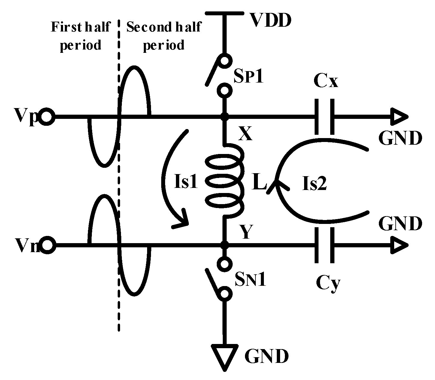
Before discussing the principle of the back-gate-biasing technique, it is worth introducing the behavior model and parasitic effect of current-reuse VCO. The behavior model of current-reused VCO is depicted in Figure 3. The circuit can operate in two states periodically. MP1 and MN1 can be simplified as switches, SP1 and SN1. Additionally, C x and C y represent equivalent capacitors in node X and node Y, respectively, including parasitic capacitors connected to LC-tank. The oscillation frequency f 0 is shown as follows:
f 0 = 1 2 π L C x = 1 2 π L C y
C x = C y = 1 2 C v a r ( V ) + 1 2 C p + 1 2 C c + C p a r
C v a r ( V ) = r m s [ i ( t ) ] | f 0 r m s ( d V ( t ) d t ) | f 0 = F ( V t u n e ± V x ( y ) )
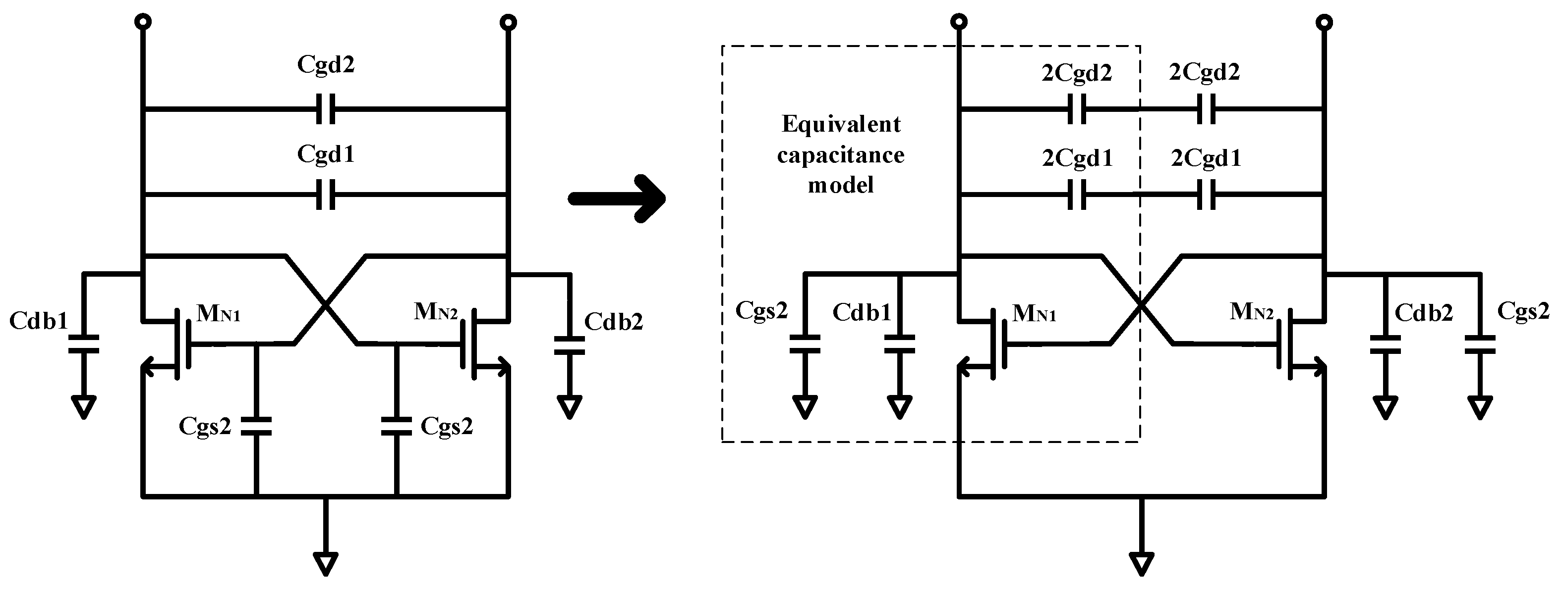
where C v a r ( V ) is the average capacitance of MOS varactor over a single period and can be calculated by the method described in [15]. C v a r ( V ) is determined by current i ( t ) of MOS varactors and voltage difference V ( t ) between the tuning voltage ( V t u n e ) and dynamic node voltage of X or Y ( V x or V y ). C p a r is the parasitic capacitors from transistors. In mm-wave application, parasitic capacitors cannot be ignored. When the size of cross-coupled pairs is large, the parasitic capacitance will be comparable with variable capacitance C v a r . According to the capacitance distribution of an MOS transistor and the Miller effect, Figure 3 presents the simplified equivalent capacitance model of the cross-coupled pairs. If the substrate is virtual ground, the parasitic capacitance C g b should be considered.
When MN1 and MN2 are equal, the equivalent parasitic capacitance can be expressed as follows:
C p a r = C g s + 4 C g d + C d b + C g b
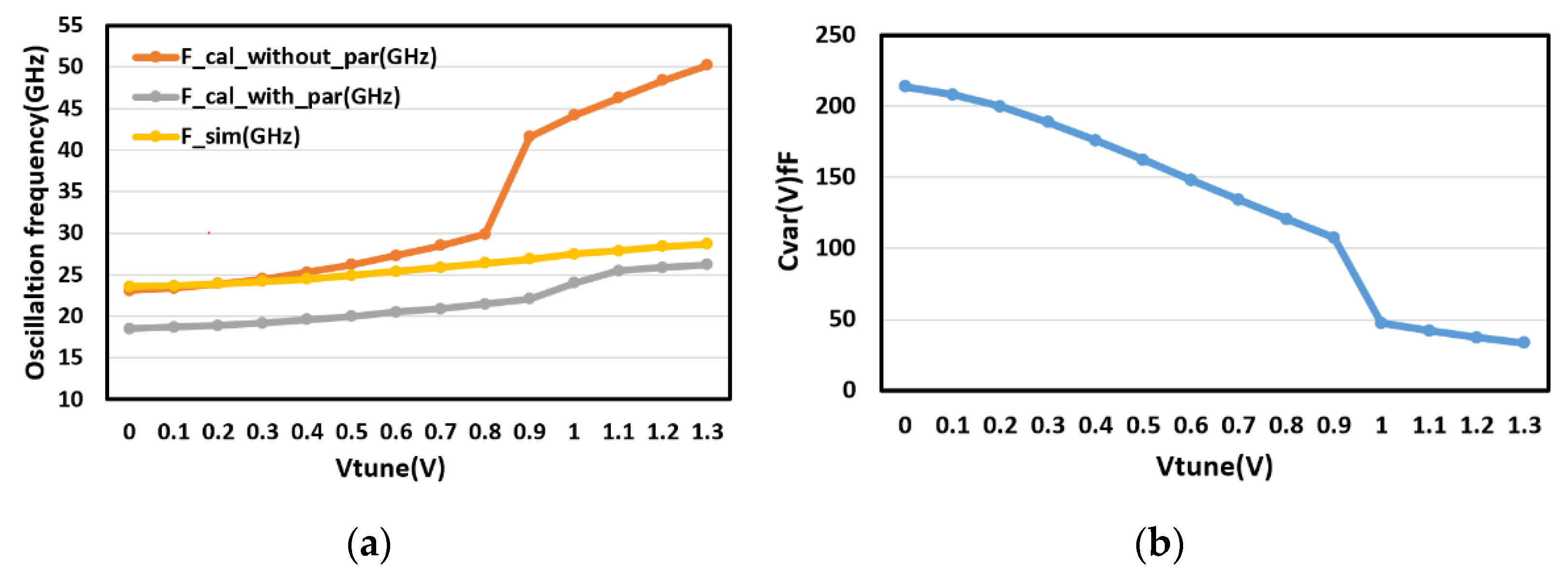
It can be seen that the parasitic capacitance introduced by the gate-drain capacitance C g d is the largest. Therefore, in the circuit layout design process, the layout should be optimized to reduce the gate-drain capacitance. Assuming that the outputs nodes V x and V y are equal, the average capacitance of varactors equivalent to the LC-tank is C v a r ( V ) / 2 . The comparison of calculation and simulation results with different tuning voltages, as shown in Figure 4a. When considering parasitic capacitance, the calculated frequency will be lower than the simulation results. On the contrary, the calculated frequency will be higher than the simulation. However, the error will increase in the high frequency cases. Figure 4a shows that there is a certain error in the model in the high frequency range. After considering the parasitic capacitance, the trend of calculation results is close to the simulation results. Figure 4b shows the average capacitance that varactors variate with tuning voltage. As V t u n e increases, C v a r ( V ) will decrease. This can explain why the frequency will drop as the tuning voltage increases.
When V o p is “low” and V o n is “high”, MP1 and MN1 are turned on simultaneously. A current path flowing from VDD to GND is formed, and as seen from Figure 4, I S 1 is the current. When V o p is “high” and V o n is “low”, the transistors are cut off, so energy stored in capacitors is used to compensate for a loss of LC-tank. From Figure 5, the current I S 2 is flowing from C x to C y instead of to the ground, achieving an effective way to decrease power consumption.
Star-up condition is a critical problem to limit the ultra-low-power VCO. There are two major ways to decrease power consumption. The first one is to decrease supply voltage, the second way is to reduce the dimension of transistors. In a word, the key to lower power is to limit the current flowing into the LC-tank. In order to limit the parasitic capacitors, the proposed VCO employs small size transistors. However, Gm-cell may not provide sufficient negative resistors. To solve this problem, an appropriate DC bias is applied to bulk to boost transconductance of the transistors. Additionally, the fixed capacitor Cp can improve the quality factor of an LC-tank [16]. However, threshold voltage will decrease to cause more power consumption. Therefore, dynamic back-gate-biasing technique is proposed to further reduce power consumption.
Here, is the basic principle of the technique. Due to the imbalance of current-reused VCO, an error voltage of node X and node Y appear in the central tap of inductor. Assuming voltage in X and Y is inverse, the error voltage is expressed as follows:
V E ( ω t ) = V p cos ( ω t ) ( V p δ V ) cos ( ω t π )
where ω is the oscillation frequency, V p is the peak amplitude and δ V is the mismatch voltage of amplitude in node X and node Y. Ideally, if the output is symmetric, δ V equals to zero and central tap behave as virtual AC ground.
The proposed VCO employs a capacitive divider to extract the error voltage VE which is passed to the bulk of negative device, so the threshold voltage periodically varies with output voltage. To explain in more detail how threshold voltage changes, Figure 6a,b show the transient simulation of PMOS and NMOS, respectively.
Due to the dynamic back-gate-biasing technique, the threshold voltage of MOS decreases to approximate 0.3 V. From Figure 6, the voltage in bulk (i.e., V B N ) is in opposite phase with that in the gate (i.e., V G N . This means that the threshold voltage will increase while cross-coupled pairs are gradually turning on. Accordingly, the transconductance of MOS decreases and the current will be limited so that less power is consumed. Although the technique can slow down the time of turning off, it can be ignored.
According to [17], the lowest available frequency is limited by the start-up condition while the highest available frequency is limited by the parasitic capacitance. In a word, the quality factor of passive components and parasitic capacitors limits the tuning range, shown as in Equation (11):
C m a x C m i n > C m a x + C p a r C m i n + C p a r
where C p a r is the parasitic capacitors. Based on Equation (8), if C p a r were comparable to value of varactors, the ratio of C m a x and C m i n will be significantly reduced. The proposed VCO can effectively reduce the parasitic capacitance by allowing transistors with small sizes. This is another advantage introduced by this technique. As mentioned above, the threshold voltage will increase when cross-coupled pairs are switched on and parasitic capacitors from transistors slightly decrease, so that the tuning range can be extended. To further minimize the parasitic capacitor, the channel lengths of the transistors, called L, are set to be shortest.

3. Post-Layout Simulation Results

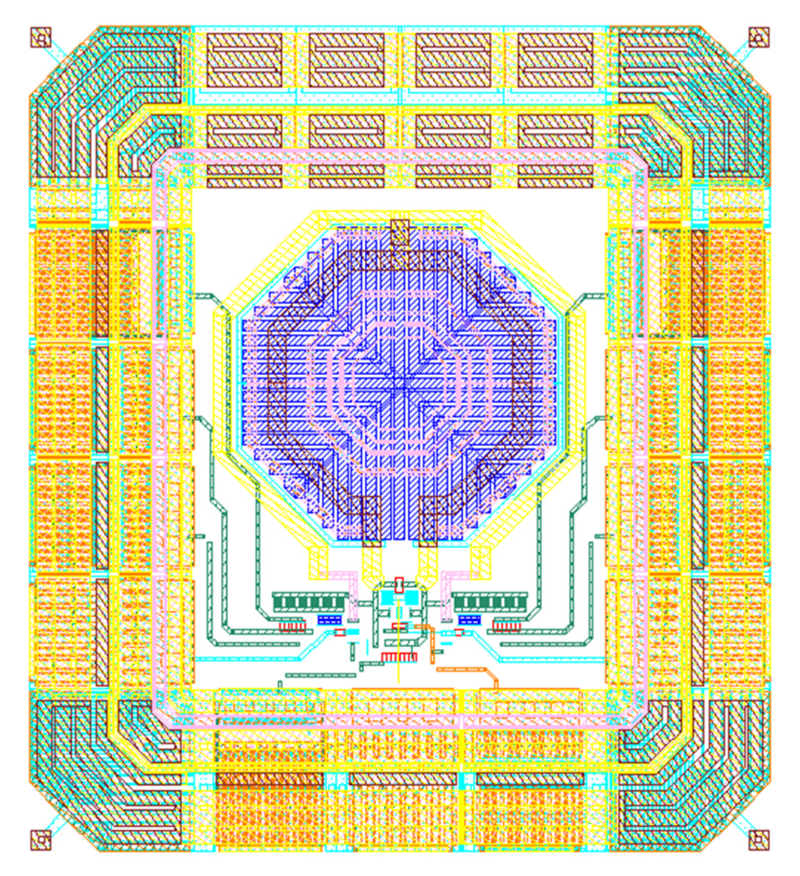
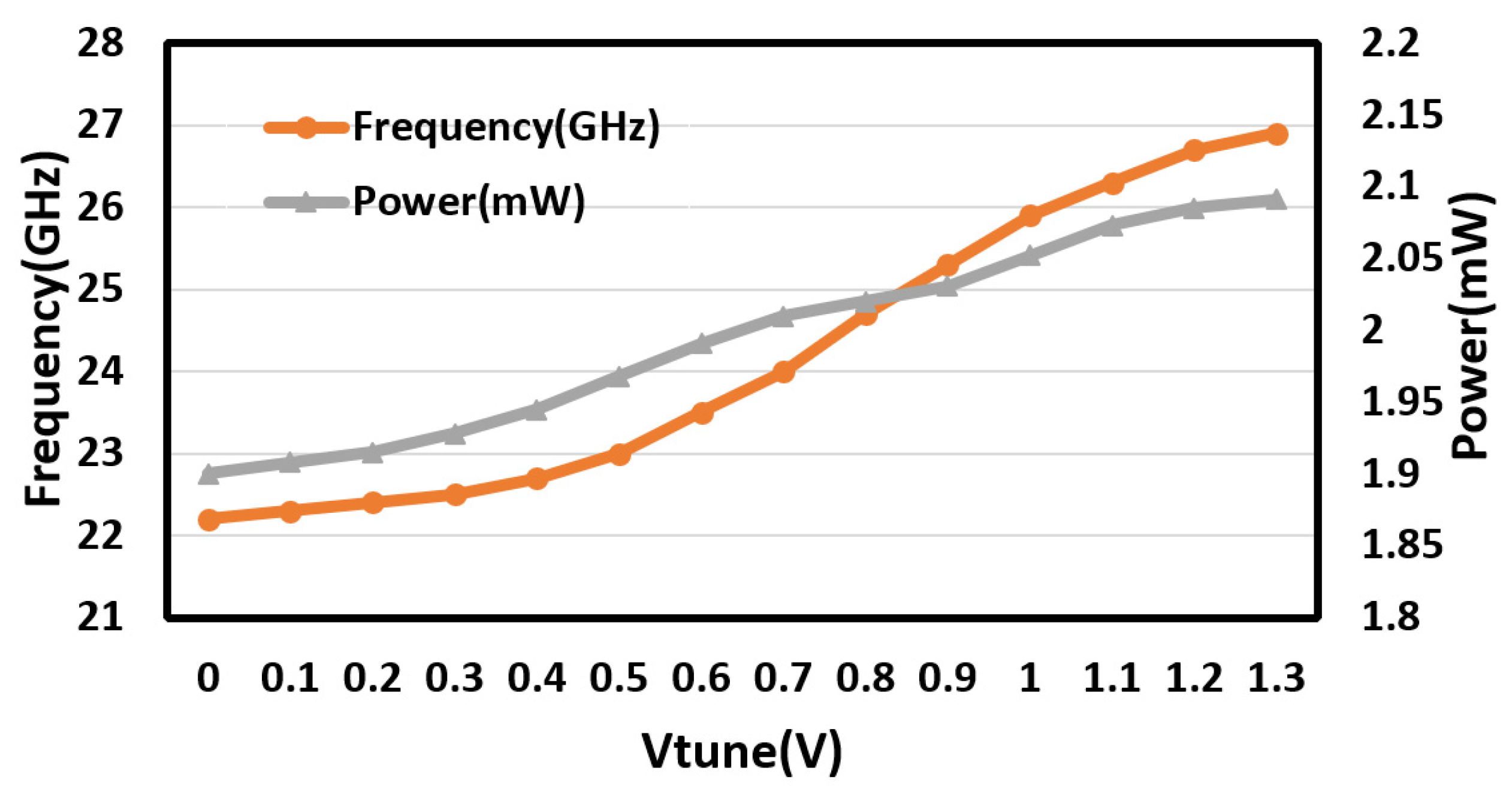
The modified LC-VCO is implemented in SMIC 55 nm 1 P7M CMOS low-power technology. It is essential to minimize the parasitic capacitors, especially parasitic capacitors of cross-coupled pairs. Figure 7 shows the whole layout, with a core area of 0.043 mm2. The oscillation frequency is tuned from 22.2 GHz to 26.9 GHz (19.1%) with the control voltage from 0 to 1.3 V. The MOS varactors operate in accumulation mode. To increase the tunning linearity, the output DC voltage should be set at an appropriate value based on the C–V characteristic of MOS varactors.
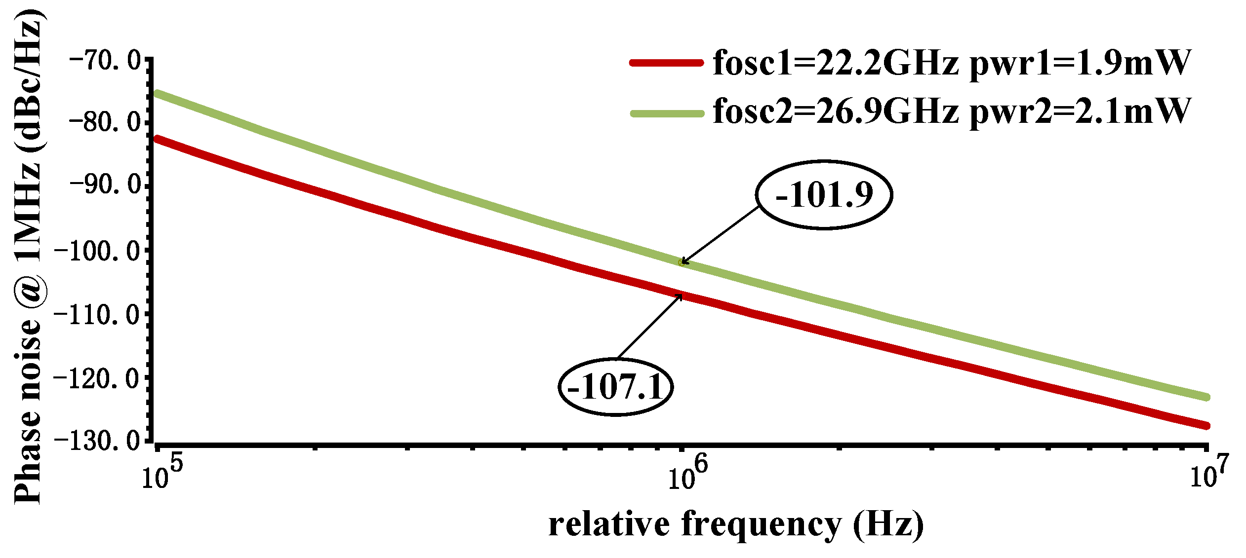
As shown in Figure 8, the phase noise at 1 MHz offset is −101.9.4 dBc/Hz at 26.9 GHz and −107.1 dBc/Hz at 22.2 GHz. In mm-wave, Q of varactors greatly limits the performance of VCOs. When the MOS varactors are working in accumulation region or depletion region, the Q of the capacitor is proportional to L 2 and L 1 , respectively [2]. To optimize the phase noise, the channel length should be the shortest.
When the VCO operates at the lowest operating frequency of 22.2 GHz, it has the minimum phase noise of −107.1 dBc/Hz and the lowest power consumption of 1.9 mW. The transient simulation is depicted in Figure 9. The proposed structure has an asymmetry differential output with an output swing of around 300 mV. The imbalance of outputs will affect the phase noise performance, so a more effective way to improve the symmetry of current-reused topology is needed. From the spectrum of output waveform, the total harmonic distortion (THD) can be calculated. Since the fundamental wave is much larger than the third harmonic, higher harmonic components are ignored and the THD can be regarded as the difference between the fundamental wave and the second harmonic component. When VCO operates in the lowest frequency. The approximate value of THD is −40.6 dB.
Figure 10 shows a measured operation frequency and power consumption in different tuning voltage from 0 V to 1.3 V. As shown in Figure 11, the output power is positively related to the tuning voltage Vtune, but the THD will deteriorate due to the increase in frequency. The proposed circuit has a THD performance of−40 dB~−19.7 dB and an output power of −6.9~−2.9 dBm over the tuning range.
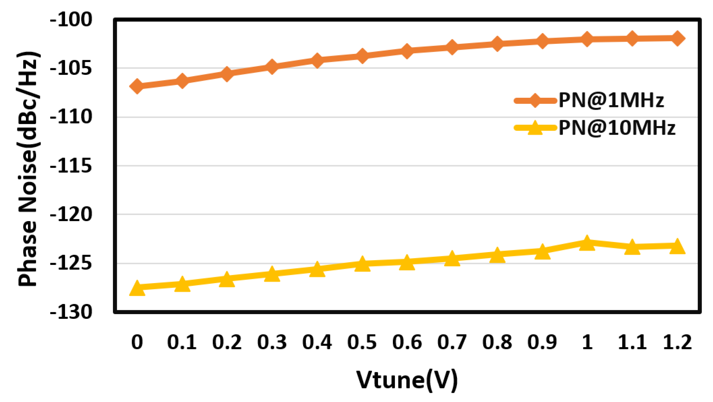
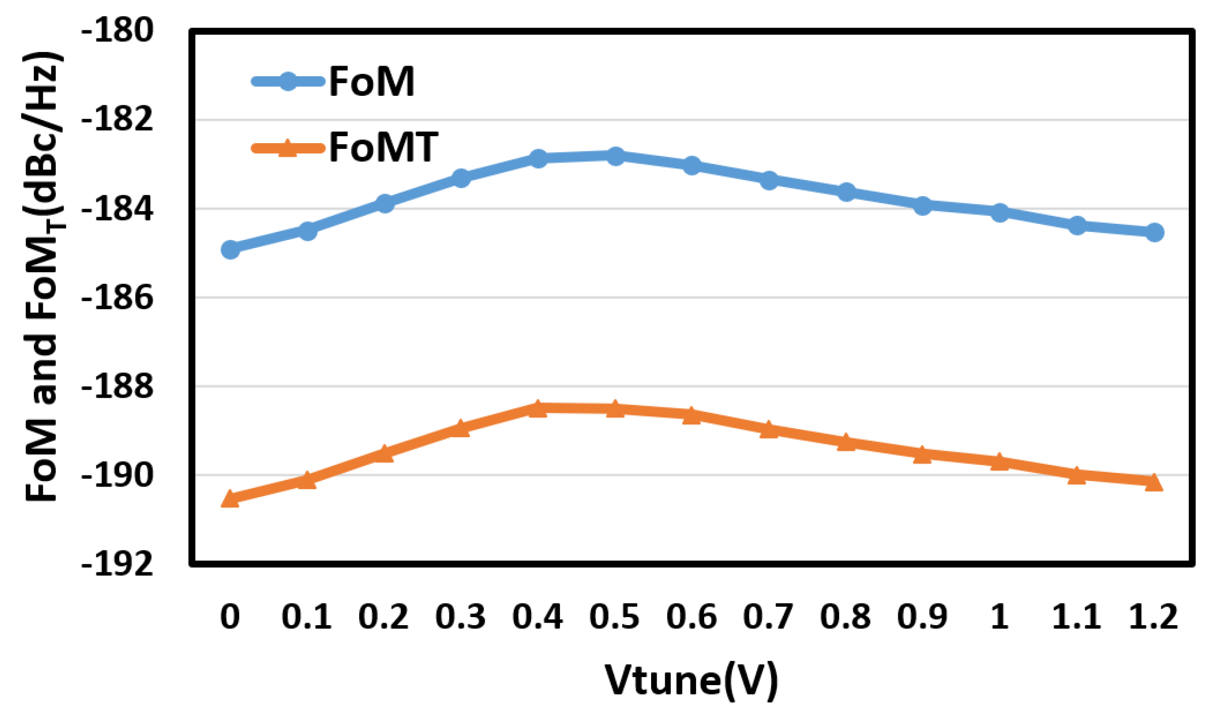
Figure 12 presents the phase noise at 1 MHz and 10 MHz offset across the tuning range. To measure the overall performance in terms of operating frequency, phase noise, power and tunning range, whilst FoM and FoMT are defined as shown in Table 1 and shown in Figure 13. At 1 MHz offset, the FoM can changes from −182.8 dBc/Hz to −185.1 dBc/Hz over the whole tuning range, while the FoMT is 5.6 dB lower than FoM. The larger the absolute value of FoM and FoMT, the better the overall performance will be. If the VCO can operate in mm-wave with low power consumption, low phase noise and wide tuning range, an excellent FoM and FoMT can be achieved. However, due to the limitations of passive components and the parasitics parameter, high FoM and FoMT are difficult to realize.
Table 1 shows the performance comparison of different state-of-the-art VCOs. Compared with these VCOs, the proposed VCO can achieve a lower power consumption and wide tuning range with a simple topology. In the mm-wave band, Q of LC-tank is determined by the varactor and capacitor array, whose Q is extremely low. At the same time, to demand a wide bandwidth, the wide tuning range of VCO is critical. The proposed VCO can realize lower power consumption with a wide tuning range without switching capacitor array while keeping the phase noise of −101~−107 at 1 MHz offset. However, the variation of phase noise is too large over the tuning range. Due to it having the simplest structure, our VCO’s area is the smallest.

4. Conclusions

A novel ultra-low-power K-band current-reuse LC-VCO with excellent balanced-amplitude was proposed, implemented using SMIC 55 nm 1 P7M CMOS low power process. Thanks to the self-adaptive capacitive feedback network, the proposed current-reuse LC-VCO achieves not only ultra-low power consumption but also a very wide tuning range. The DC biasing technique was used to start up the VCO, thereby ensuring that small dimension transistors can be used. When cross-couple pairs are turned on, the feedback network is used to extract the output error voltage V E ( ω t ) and reduce the threshold voltages, resulting in very low dynamic power consumption. At the same time, the small-sized transistors reduce the influence of parasitic capacitors, a wider tuning range can be gained. This ultra-low-power consumption VCO can be applied in various fields such as low-power dissipation PLLs, and frequency triplers. Since the experimental results are only post-layout simulation, a further tape-out test is needed to verify the reliability of the circuit.

Author Contributions

Conceptualization, X.D.; funding acquisition, X.D.; methodology, X.D. and P.T.; validation, X.D.; writing—original draft, P.T.; writing—review and editing, X.D. All authors have read and agreed to the published version of the manuscript.

Funding

This research was funded by National Natural Science Foundation of China, grant number 62071306; Natural Science Foundation of Guangdong, grant number 2020A1515011482; Science and Technology Innovation Foundation of Shenzhen, grant number JCYJ20200109113601723.

Conflicts of Interest

The authors declare no conflict of interest.

References

  1. Jahan, N.; Baichuan, C.; Pokharel, R.K.; Barakat, A. A K-Band VCO Employing High Active Q-factor Defected Ground Structure Resonator in 0.18 um CMOS Technology. In Proceedings of the 2018 IEEE International Symposium on Circuits and Systems (ISCAS), Florence, Italy, 27–30 May 2018; pp. 1–5. [Google Scholar] [CrossRef]
  2. Andreani, P.; Mattisson, S. On the use of MOS varactors in RF VCOs. IEEE J. Solid-State Circuits 2000, 35, 905–910. [Google Scholar] [CrossRef]
  3. Mazzanti, A.; Andreani, P. A Push–Pull Class-C CMOS VCO. IEEE J. Solid-State Circuits 2013, 48, 724–732. [Google Scholar] [CrossRef]
  4. Guo, H.; Chen, Y.; Mak, P.; Martins, R.P. A 0.083-mm2 25.2-to-29.5 GHz Multi-LC-Tank Class-F234 VCO with a 189.6-dBc/Hz FOM. IEEE Solid-State Circuits Lett. 2018, 1, 86–89. [Google Scholar] [CrossRef]
  5. Huang, Y.; Chen, Y.; Guo, H.; Mak, P.-I.; Martins, R.P. A 3.3-mW 25.2-to-29.4-GHz Current-Reuse VCO Using a Single-Turn Multi-Tap Inductor and Differential-Only Switched-Capacitor Arrays with a 187.6-dBc/Hz FOM. IEEE Trans. Circuits Syst. I Regul. Pap. 2020, 67, 3704–3717. [Google Scholar] [CrossRef]
  6. Hu, Y.; Siriburanon, T.; Staszewski, R.B. A Low-Flicker-Noise 30-GHz Class-F23 Oscillator in 28-nm CMOS Using Implicit Resonance and Explicit Common-Mode Return Path. IEEE J. Solid-State Circuits 2018, 53, 1977–1987. [Google Scholar] [CrossRef] [Green Version]
  7. Yun, S.-J.; Shin, S.-B.; Choi, H.-C.; Lee, S.-G. A 1mW current-reuse CMOS differential LC-VCO with low phase noise. In Proceedings of the ISSCC, 2005 IEEE International Digest of Technical Papers, Solid-State Circuits Conference, San Francisco, CA, USA, 10 February 2005; Volume 1, pp. 540–616. [Google Scholar] [CrossRef]
  8. Guo, S.; Gui, P.; Liu, T.; Zhang, T.; Xi, T.; Wu, G.; Fan, Y.; Morgan, M. A Low-Voltage Low-Phase-Noise 25-GHz Two-Tank Transformer-Feedback VCO. IEEE Trans. Circuits Syst. I Regul. Pap. 2018, 65, 3162–3173. [Google Scholar] [CrossRef]
  9. Fu, Y.; Li, L.; Wang, D.; Wang, X.; He, L. 28-GHz CMOS VCO With Capacitive Splitting and Transformer Feedback Techniques for 5G Communication. IEEE Trans. Very Large Scale Integr. (VLSI) Syst. 2019, 27, 2088–2095. [Google Scholar] [CrossRef]
  10. MKashani, H.; Molavi, R.; Mirabbasi, S. A 2.3-mW 26.3-GHz Gm-Boosted Differential Colpitts VCO with 20% Tuning Range in 65-nm CMOS. IEEE Trans. Microw. Theory Tech. 2019, 67, 1556–1565. [Google Scholar] [CrossRef]
  11. Murphy, D.; Darabi, H. A 27-GHz Quad-Core CMOS Oscillator with No Mode Ambiguity. IEEE J. Solid-State Circuits 2018, 53, 3208–3216. [Google Scholar] [CrossRef]
  12. Shu, Y.; Qian, H.J.; Luo, X. 17.4 A 18.6-to-40.1GHz 201.7dBc/Hz FoMT Multi-Core Oscillator Using E-M Mixed-Coupling Resonance Boosting. In Proceedings of the 2020 IEEE International Solid-State Circuits Conference-(ISSCC), San Francisco, CA, USA, 16–20 February 2020; pp. 272–274. [Google Scholar] [CrossRef]
  13. Wei, M.; Chang, S.; Huang, S.; Yang, Y.; Negra, R. Investigation of Sub-Milliwatt Current-Reuse VCOs with Mono-Spontaneous Transconductance Match Technique. IEEE Trans. Microw. Theory Tech. 2014, 62, 332–340. [Google Scholar] [CrossRef]
  14. Razavi, B. RF Microelectronics. Prentice Hall Communications Engineering Emerging Technologies; Pearson: London, UK, 1998. [Google Scholar]
  15. Bunch, R.L.; Raman, S. Large-signal analysis of MOS varactors in CMOS-Gm LC VCOs. IEEE J. Solid-State Circuits 2003, 38, 1325–1332. [Google Scholar] [CrossRef]
  16. Toso, S.D.; Bevilacqua, A.; Gerosa, A.; Neviani, A. A thorough analysis of the tank quality factor in LC oscillators with switched capacitor banks. In Proceedings of the 2010 IEEE International Symposium on Circuits and Systems, Paris, France, 30 May–2 June 2010; pp. 1903–1906. [Google Scholar] [CrossRef]
  17. Sadhu, B.; Kim, J.; Harjani, R. A CMOS 3.3-8.4 GHz wide tuning range, low phase noise LC VCO. In Proceedings of the 2009 IEEE Custom Integrated Circuits Conference, San Jose, CA, USA, 13–16 September 2009; pp. 559–562. [Google Scholar] [CrossRef]
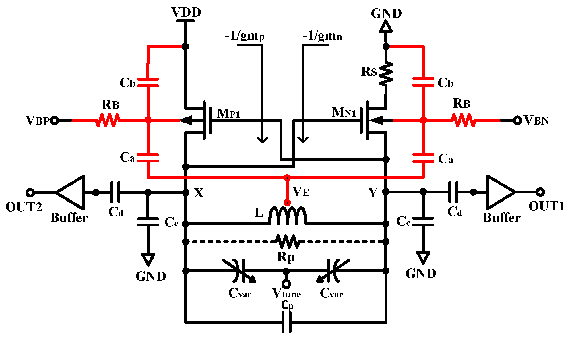
Figure 1. Schematic of the proposed current-reuse voltage-controlled oscillator (VCO).
Electronics 10 00889 g001
Figure 2. Schematic of the proposed current-reuse VCO.
Electronics 10 00889 g002
Figure 3. The simplified equivalent capacitance model of the cross-coupled pairs.
Electronics 10 00889 g003
Figure 4. (a) Calculation and simulation results of oscillation frequency under different tuning voltage; (b) average capacitance under different tuning voltage.
Electronics 10 00889 g004
Figure 5. Behavior model of current-reuse VCO.
Electronics 10 00889 g005
Figure 6. Transient simulation of gate, bulk and central tap: (a) PMOS and (b) NMOS.
Electronics 10 00889 g006
Figure 7. The layout of the proposed VCO.
Electronics 10 00889 g007
Figure 8. Phase noise of VCO at 22.2 GHz and 26.9 GHz.
Electronics 10 00889 g008
Figure 9. Post-layout simulation of VCO in minimum oscillation frequency and its spectrum.
Electronics 10 00889 g009
Figure 10. Operation frequency and power vs. tuning range.
Electronics 10 00889 g010
Figure 11. THD and output power vs. tuning range.
Electronics 10 00889 g011
Figure 12. Phase noise vs. frequency.
Electronics 10 00889 g012
Figure 13. FoM and FoMT vs. frequency.
Electronics 10 00889 g013
Table 1. Performance summary of different VCOs.
This Work *[5][6][9][10][11]
Process (nm)556528656540
Supply (V)1.21.110.910.95
Tuning range22.2~26.925.2~29.3827.3~31.226.526.323~29.9
TR (%)19.115.3NA1420.126.1
Area (mm2)0.0430.1160.150.220.220.1
Power (mW)1.9~2.13.03~3.4422~2310.82.316
PNoise@1 MHz (dBc/Hz)−107~−101−104~−103.9−106~−104−105.8−121−110
PNoise@10 MHz (dBc/Hz)−127.7~−122.9−123.5~−122.5−125~−126−130NANA
FoM@1 MHz (dBc/Hz) 1−182.8~−185.1−187.3~−187.6−184~−183−184−191.8−187~−186.5
FoMT@1 MHz (dBc/Hz) 2−188.4~−190.7−191.3~−190.9−184NANA−195.3~−194.8
* all the data of this work are the post-layout simulation results. 1 F o M = L { ω } 20 log ( ω 0 ω ) + 10 log ( P d c 1 mW ) ; 2 F o M T = F o M 20 log ( T R 10 % ) .
Publisher’s Note: MDPI stays neutral with regard to jurisdictional claims in published maps and institutional affiliations.