Article

K-Band Hetero-Stacked Differential Cascode Power Amplifier with High Psat and Efficiency in 65 nm LP CMOS Technology

1
Department of Electrical and Computer Engineering, Sungkyunkwan University, 2066 Seobu-ro, Jangan-gu, Suwon 16419, Gyeonggi-do, Korea
2
Teledyne Scientific and Imaging LLC, Thousand Oaks, CA 91360, USA
3
Department of Semiconductor Systems Engineering, Sungkyunkwan University, 2066 Seobu-ro, Jangan-gu, Suwon 16419, Gyeonggi-do, Korea
*
Author to whom correspondence should be addressed.
Electronics 2021, 10(8), 890; https://doi.org/10.3390/electronics10080890
Submission received: 16 March 2021 / Revised: 3 April 2021 / Accepted: 6 April 2021 / Published: 8 April 2021
(This article belongs to the Section Microwave and Wireless Communications)

Abstract

:
A K-band complementary metal-oxide-semiconductor (CMOS) differential cascode power amplifier is designed with the thin-oxide field effect transistor (FET) common source (CS) stage and thick-oxide FET common gate (CG) stage. Use of the thick-oxide CG stage affords the high supply voltage to 3.7 V and enables the high output power. Additionally, simple analysis shows that the gain degradation due to the low cut-off frequency of the thick-oxide CG FET can be compensated by the high output resistance of the thick-oxide FET if the inter-stage node is neutralized. The measured results of the proposed power amplifier demonstrate the saturated output power of the 23.3 dBm with the 31.3% peak power added efficiency (PAE) at 24 GHz frequency. The chip is fabricated in 65-nm low power (LP) CMOS technology and the chip size including all pads is 700 μm × 630 μm.

1. Introduction

Rapid scaling of CMOS technology enables the mm-wave transceiver design including 5G mobile communications and automotive radar applications. Despite many advantages of the CMOS process, such as high-density integration of radio frequency (RF) and digital building blocks and low-cost mass manufacturing capability, the output power degradation due to the low breakdown voltage of highly scaled CMOS devices is a serious weakness for the design of RF power amplifiers. Accordingly, various design approaches for CMOS power amplifiers have been studied to achieve high efficiency and output power. Series voltage or parallel current combining techniques are essential to obtain high output power. Another approach to increase the output power is to stack the FETs for high voltage swing [1]. The larger the number of cascoded transistors increase, the higher the supply voltage can be used. Accordingly, the maximum output power also increases. However, the available number of stacked FETs is not unlimited due to breakdown issues in the common gate (CG) stage [2].
This paper presents a K-band differential power amplifier using the hetero-stacked cascode structure adopting two different gate oxide thicknesses. The common source (CS) stage uses a normal field effect transistor (FET) with the shortest gate length available from the process for high current driving capability, and the CG stage uses the thick-oxide FET for the high voltage swing. Though the hetero-stacked cascode power amplifier (PA) has been used for low GHz applications in a single-ended fashion [3], the PA above the X-band has not adopted this structure because of gain and efficiency degradation due to the low cut-off frequency of the thick-oxide FET. This work shows that the high gain as well as the high output power can be achieved near the cut-off frequencies of the thick CG FET by neutralizing the inter-stage node for the hetero-stacked cascode amplifier.

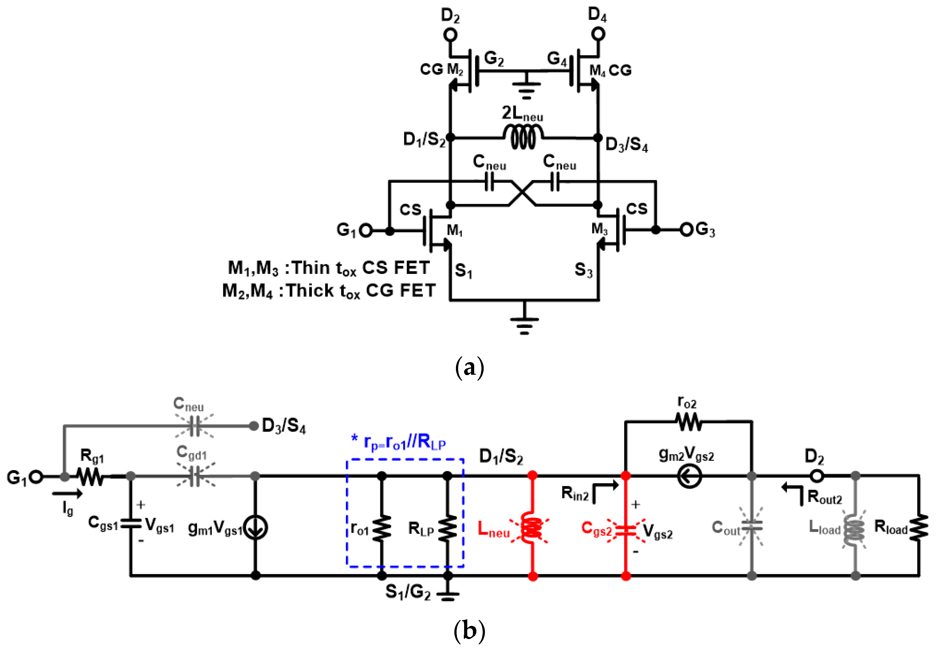
2. High Frequency Gain of the Neutralized Hetero-Stacked Cascode Amplifier

The thick-oxide common gate (CG) field effect transistor (FET) used in the cascode amplifier can enhance the output power by allowing a high supply voltage without multi-stage stacking. However, as the operation frequency increases, the efficiency and gain tend to more rapidly decrease because of the lower inter-stage pole frequency due to the smaller transconductance of the thick-oxide CG FET than the thin-oxide CG FET. But, examining the maximum available gain (MAG) of the cascode amplifier, neutralizing the inter-stage capacitances can surprisingly mitigate the effect of the cut-off frequency of the CG FET on the MAG.
Figure 1a shows the hetero-stacked cascode power amplifier with a shunt inductor neutralization. The MAG of the neutralized cascode cell can be derived based on the small signal equivalent half circuit of the cascode cell shown in Figure 1b. The value of Lneu for compensating Cgs2 is determined by the resonance condition. For the differential amplifier design in mm-wave range, the stability of the common source (CS) FET is enforced by using the cross-coupled capacitor Cneu, which achieves infinite isolation between the input and output of the CS FET as in [4]. Assuming the perfect neutralization as explained in [4], we simplified the analysis to calculate the MAG of the cascode cell ignoring Cgd1. At first, the available source power (Pavs) is given by (Equation (1)).
P a v s = I g 2 R g 1 2
Assuming the shunt neutralization at the input of the CG FET, the output resistance of the cascode cell is given by (Equation (2)) [5]. Under the conjugate matching condition at the output, the input resistance Rin2 of the CG FET is determined by (Equation (3)) as explained in [5].
R o u t 2 = ( r o 2 + r p ( 1 + g m 2 r o 2 ) ) g m 2 r p r o 2
R i n 2 = r o 2 + R o u t 2 / 2 1 + g m 2 r o 2 = r o 2 1 + g m 2 r o 2 + r p 2 1 g m 2 + r p 2
In (Equations (2) and (3)), the resistance rp is a parallel equivalent resistance combining ro1 and RLP. Then the available output power (Pavo) is given by (Equation (4)). The input current of the CG FET from the output current of the CS FET can be determined by current division between Rin2 and rp. Additionally, the output resistance Rout2 and the load resistance Rload equally share the output current of the cascode cell under conjugate matching condition, a half of the output current of CG FET is delivered to Rload. In (Equation (5)), the Pavo is expressed in terms of the input current instead of the voltage Vgs1 since the available source power is expressed using the input current Ig. The Pavo in (Equation (6)) is obtained by using (Equations (2) and (3)) for Rout2 and Rin2 in (Equation (5)) at the neutralizing frequency f0.
P a v o = 1 2 ( 1 2 g m 1 V g s 1 r p R i n 2 + r p ) 2 R o u t 2
= 1 8 ( g m 1 I g 2 π f 0 C g s 1 r p R i n 2 + r p ) 2 R o u t 2
= 1 2 I g 2 ( f t 1 f 0 ) 2 g m 2 3 r p 3 r o 2 ( 2 + 3 g m 2 r p ) 2
Introducing the quality factor Qint (=2πf0Cgs2rp) at the inter-stage node excluding Rin2, the final Pavo is obtained as follows.
P a v o = 1 2 I g 2 ( f t 1 f 0 ) 2 ( Q int f t 2 f 0 ) 3 r o 2 ( 2 + 3 Q int ( f t 2 / f 0 ) ) 2
In (Equation (7)), ft1 and ft2 are cut-off frequencies of CS and CG FET given by gm1/2πCgs1 and gm2/2πCgs2, respectively. The final Pavo (Equation (7)) is expressed using the cut-off frequency of FETs and neutralization frequency to evaluate and compare the effect of neutralization in terms of the cut-off frequency of the CG FET.
The resistance RLP is a parallel equivalent resistance of the neutralizing inductor Lneu given by
R L P = R L S ( 1 + Q L 2 ) = 2 π f 0 L n e u Q L ( 1 + Q L 2 ) Q L 2 π f 0 C g s 2
where QL is the quality factor of the neutralizing inductor. As seen in (Equation (8)), RLP decreases as the operation frequency increases, considering that the available maximum Q factor of the inductor in CMOS process is limited. Finally, MAG is obtained as the ratio of Pavo and Pavs as follows.
M A G = ( f t 1 f 0 ) 2 ( Q int f t 2 f 0 ) 3 r o 2 / R g 1 ( 2 + 3 Q int ( f t 2 / f 0 ) ) 2
When the operation frequency satisfies the following condition,
f 0 < < Q int f t 2
The MAG at the neutralizing frequency can be approximated as (Equation (11)).
M A G ( f t 1 f 0 ) 2 ( Q int f t 2 f 0 ) r o 2 9 R g 1
The result of (Equation (11)) implies that the MAG of the neutralized cascode cell is linearly proportional to ft2, unlike the quadratic dependence on ft1 of the CS FET. This behaviour is valid regardless of the gate lengths of CG FETs. It means that the effect of ft2 on the total gain of the cascode cell appears relatively smaller than ft1. Especially, the high output resistance of the thick-oxide CG FET additionally compensates the low cut-off frequency of its own. Since the cut-off frequency and the output resistance of CMOS FET are inversely and proportionally dependent on the gate length, the overall gain of the cascode cell using the thick-oxide CG stage is almost comparable to that using all thin-oxide FETs around the neutralizing frequency while the condition (Equation (10)) holds. In fact, the node Q factor Qint initially increases with neutralizing frequency because the resistance rp is dominated by ro1 at low frequencies. However, as the frequency goes high, the resistance rp gradually decreases with the neutralizing frequency due to the relation (Equation (8)). Therefore, Qint eventually saturates to the constant value and gain compensation by neutralization is relaxed.
The MAGs of two cascode cells based on (Equation (9)) are compared in Figure 2 as a function of the neutralizing frequency using extracted equivalent circuit parameters of two cascode cells using the same widths for CS/CG FETs and bias current conditions. In the relatively low frequency, the hetero-stacked cascode cell shows the higher gain up to 1.7 dB compared to the normal cascode cell because of the sufficient compensation by the Qint and high output resistance of thick-oxide CG FET. As neutralization frequency increases, the MAGs become similar and finally the normal cascode cell shows a higher gain above 90 GHz.

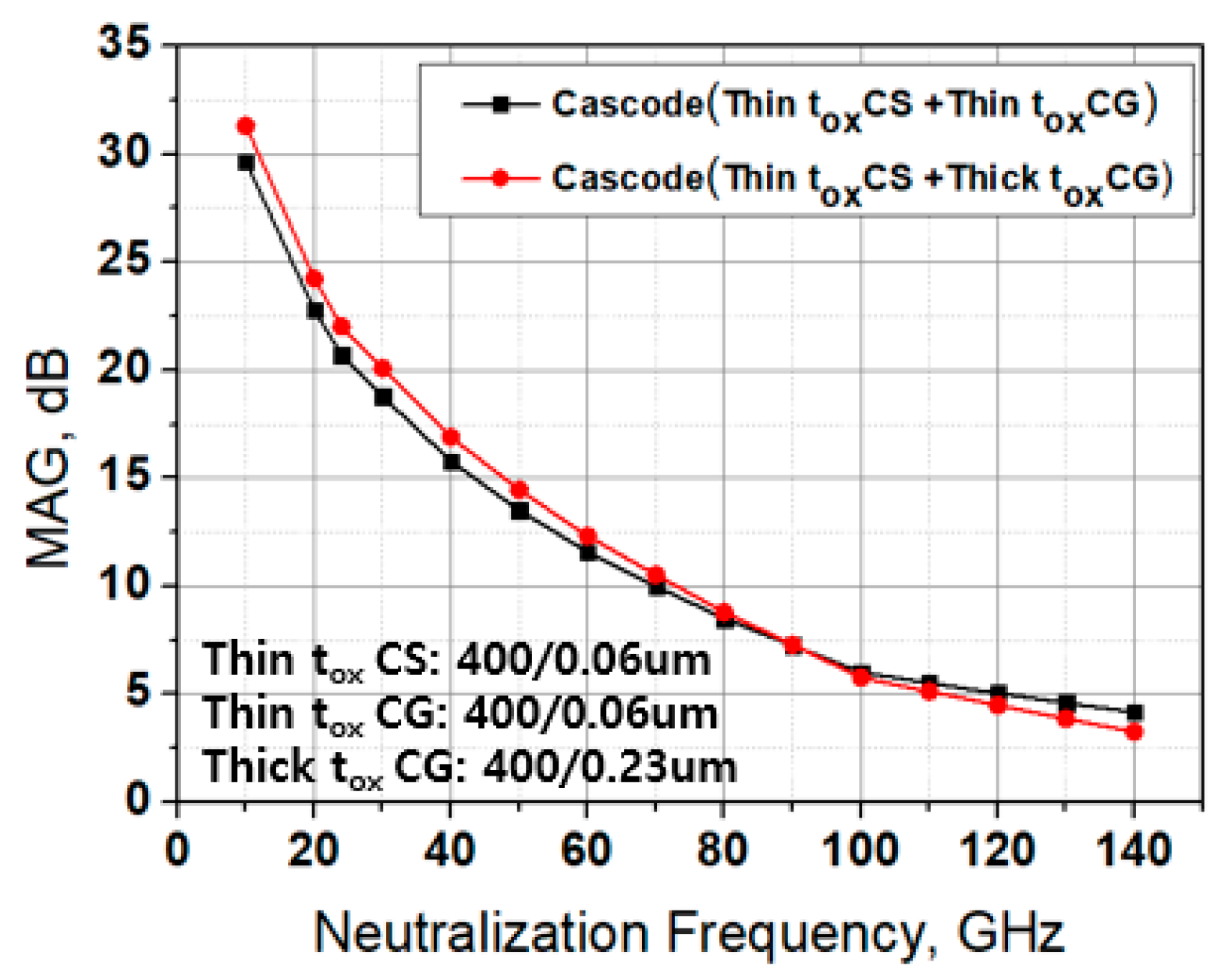
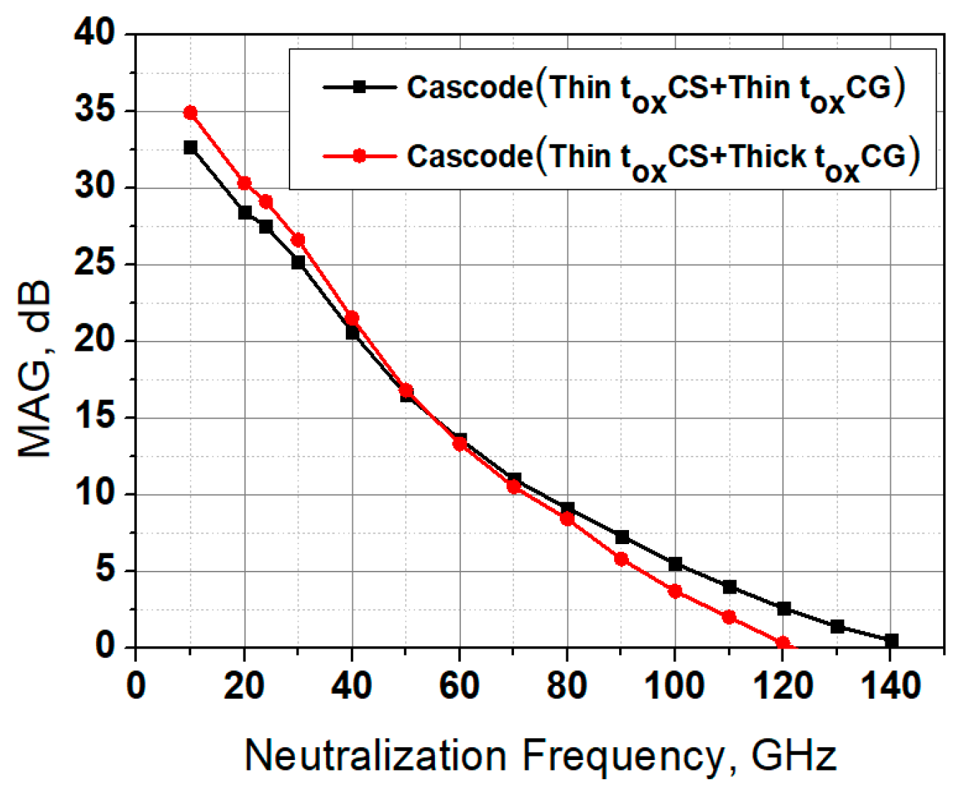
3. MAG Simulation Verification

Figure 3 shows the schematic of the proposed differential hetero-stacked cascode power amplifier composed of the thin-oxide common source (CS) field effect transistor (FET), thick-oxide common gate (CG) FET, and neutralization inductor Lneu. The differential architecture is chosen for easy neutralization compared to the single-ended structure and an additional capacitive neutralization for the CS stage.
According to the accurate simulation, the hetero-stacked cascode cell without neutralization shows the higher gain below 19 GHz because of the higher output resistance of the thick-oxide CG FET, and the inter-stage pole is negligible at low frequencies as shown in Figure 4a. However, the maximum available gain (MAG) of the hetero-stacked cascode cell without inductive neutralization is lower than that of the normal cascode cell by 3.5 dB at 24 GHz. Adopting neutralization at 24 GHz for both cascode cells, the hetero-stacked cascode shows the higher MAG up to 34 GHz and 1.5 dB higher MAG than normal cascode cell at 24 GHz as shown in Figure 4b.
Figure 5 shows the simulation results of the MAGs when neutralization is performed at every frequency to confirm the previous analysis. Results of Figure 5 consider all parasitics of passive networks using full-wave electromagnetic simulation. Increasing neutralization frequency by reducing the value of Lneu of the same component QL-value, the gain cross-over frequency is found to be approximately 60 GHz, which is slightly lower than the predicted in Figure 2. It is because the simple small signal model presented by Figure 1b ignores additional parasitic capacitances of the real cascode cells. However, surprisingly, the hetero-stacked cascode cell shows the higher gain than the normal cascode cell even beyond the cut-off frequency about 40 GHz of the thick-oxide CG FET. This result shows that the low cut-off frequency of thick-oxide FET is compensated by its high output resistance.

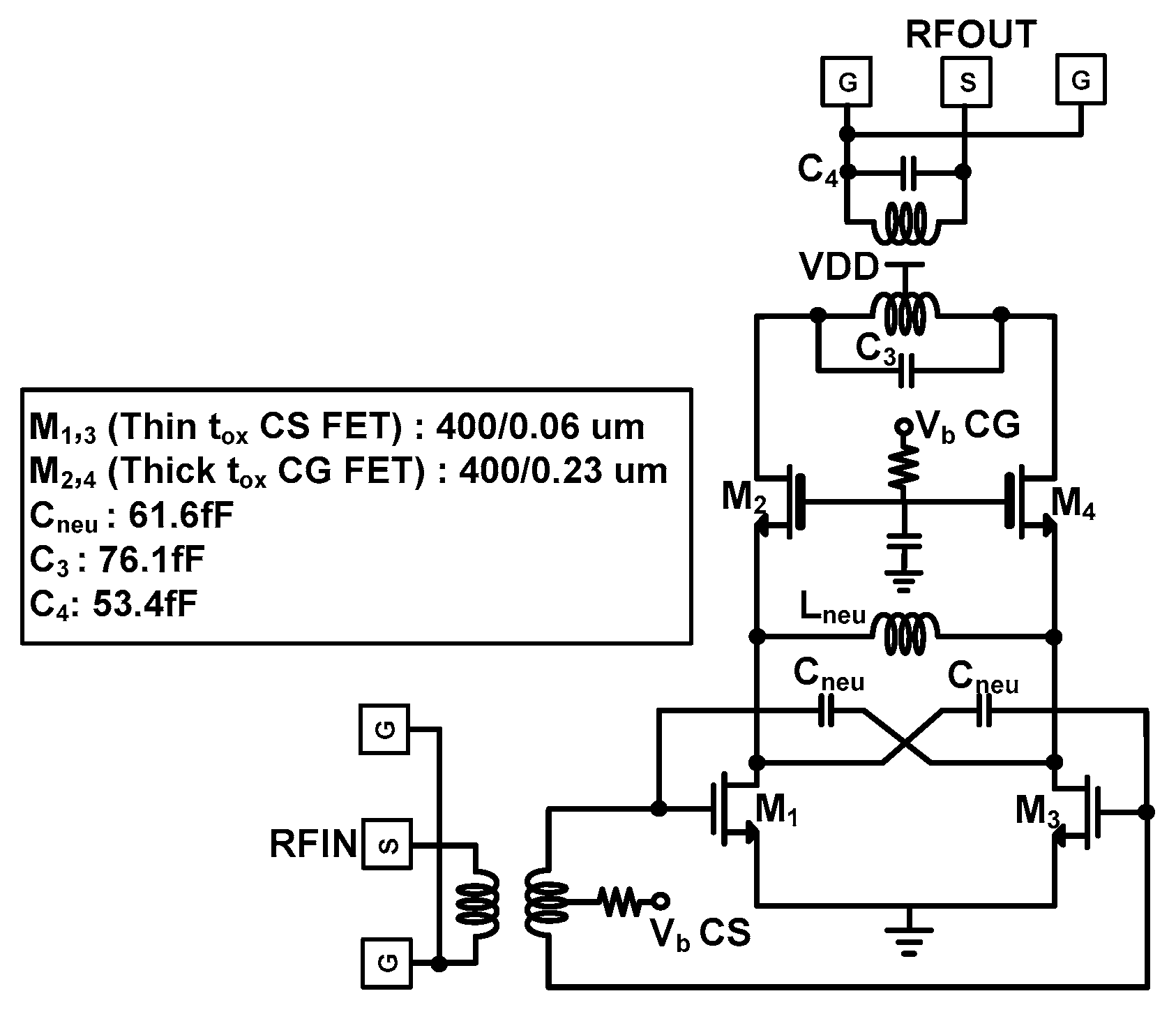
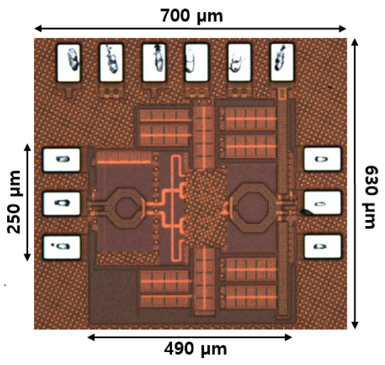
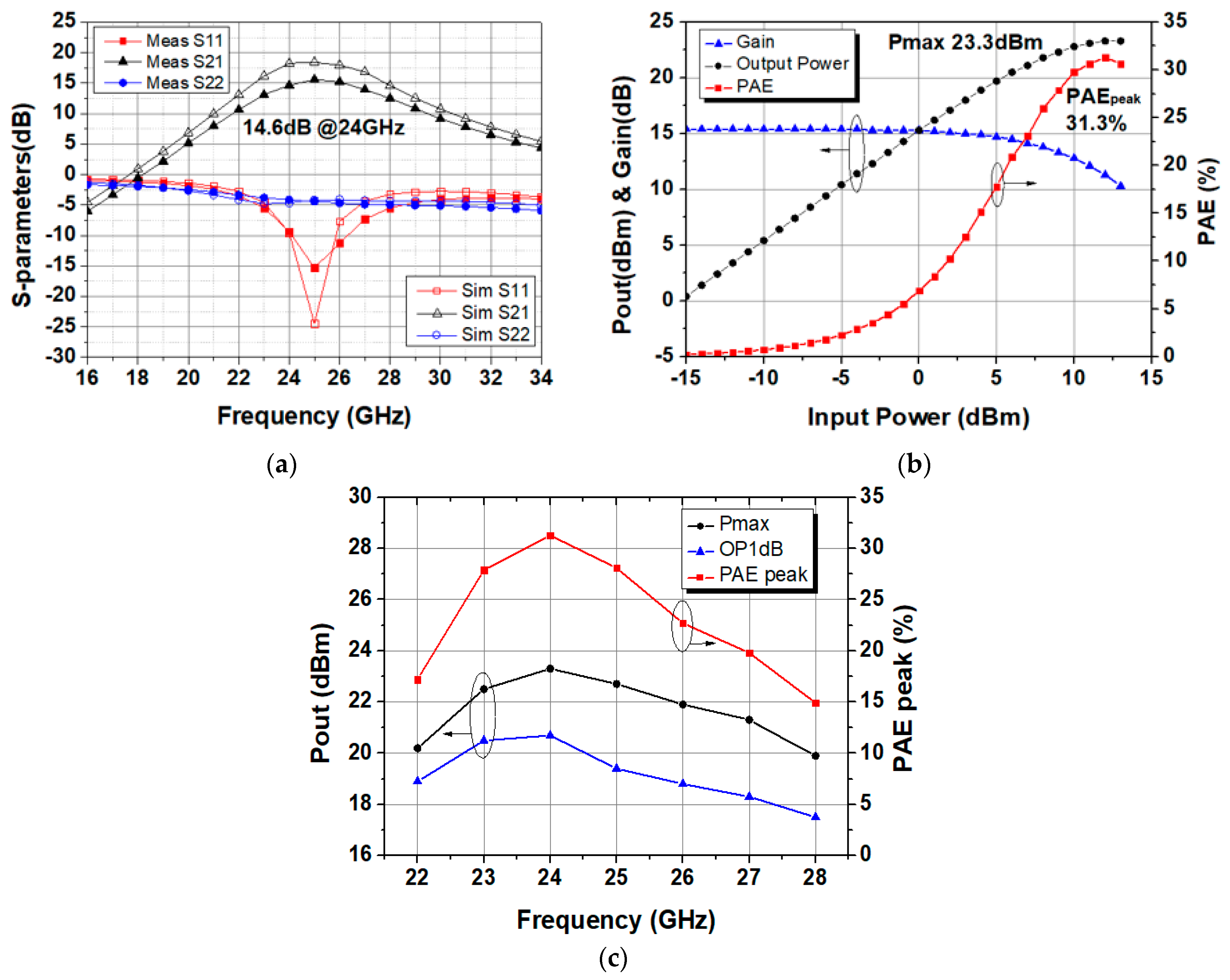
4. Measurement Results

The chip microphotograph is shown in Figure 6. The chip size is 0.7 × 0.63 mm2 including all pads. The proposed PA is fabricated using 65-nm low power (LP) CMOS technology with 0.57 mA/um current density and 1-poly 8-metal layers. The supply voltage is 3.7 V and DC power dissipation is 466 mW under quiescent condition.
Measured and simulated S-parameters are plotted in Figure 7a. The measured small signal gain is 14.6 dB and the input return loss is −9.4 dB for 24 GHz. Figure 7b shows the measured power gain, output power, and power added efficiency (PAE) of the proposed PA with a 24 GHz 1-tone continuous wave (CW) signal. The large signal measurement results demonstrate 15.4 dB gain, saturated output power of 23.3 dBm, output 1-dB compression point of 20.8 dBm, and peak PAE of 31.3% at 24 GHz. The large signal performance versus different frequencies is shown in Figure 7c from 22 GHz to 28 GHz.
Performance comparison with recent state-of-art K-band CMOS PAs is shown in Table 1.
Though the higher output powers were reported in [6,9,10], they were obtained utilizing the parallel power combining techniques for unit amplifiers. Since the proposed hetero-stacked cascode power amplifier only used a unit amplifier and N-way combining can be used for more output power.

5. Conclusions

In this paper, a K-band hetero-stacked cascode CMOS PA with high saturated output power and efficiency is presented. The PA is fabricated in 65-nm low power (LP) CMOS process stacking the thin-oxide field effect transistor (FET) and thick-oxide FET for cascode configuration with neutralization. The hetero-stacked cascode structure can enhance the output power by using a high supply voltage compared to the normal cascode structure. But using a hetero-stacked cascode in the mm-wave range, the high frequency gain degradation occurs due to low cut-off frequency of the thick-oxide common gate (CG) FET. If the inductive neutralization is applied to the inter-stage of the hetero-stacked cascode cell as used in this work, the high frequency gain degradation can be compensated by high output resistance of the thick-oxide CG FET. Additionally, this work analyses the effect of inter-stage neutralization on the gain improvement of the cascode cell. The analysis shows that the proposed cascode amplifier provides a comparable gain to the normal cascode amplifier near the cut-off frequency of the thick-oxide CG FET. The proposed cascode structure is advantageous to easily enhance the output power without gain degradation and complicated power combining techniques in the mm-wave range.

Author Contributions

Conceptualization, K.-J.C. and B.-S.K.; methodology, S.-K.K.; software, J.-H.P.; validation, K.-J.C. and S.-K.K.; formal analysis, K.-J.C., J.-H.P., and B.-S.K.; investigation, K.-J.C.; resources, J.-H.P.; data curation, K.-J.C. and B.-S.K.; writing—original draft preparation, K.-J.C.; writing—review and editing, K.-J.C. and B.-S.K.; visualization, B.-S.K.; supervision, B.-S.K.; project administration, B.-S.K.; funding acquisition, B.-S.K. All authors have read and agreed to the published version of the manuscript.

Funding

This work was supported in part by the Aerospace Parts Research and Development Program, Ministry of Trade, Industry, and Energy, under Grant (20002712).

Conflicts of Interest

The authors declare no conflict of interest.

References

  1. Lei, M.F.; Tsai, Z.M.; Lin, K.Y.; Wang, H. Design and analysis of stacked power amplifier in series-input and series-output configuration. IEEE Trans. Microw. Theory Tech. 2007, 55, 2802–2812. [Google Scholar] [CrossRef]
  2. Chen, J.H.; Helmi, S.R.; Azadegan, R.; Aryanfar, F.; Mohammadi, S. A broadband stacked power amplifier in 45-nm CMOS SOI technology. IEEE J. Solid State Circuits. 2013, 48, 2775–2784. [Google Scholar] [CrossRef]
  3. Apostolidou, M.; van der Heijden, M.P.; Leenaerts, D.M.W.; Sonsky, J.; Heringa, A.; Volokhine, I. A 65 nm CMOS 30 dBm class-E RF power amplifier with 60% power added efficiency. In Proceedings of the 2008 IEEE Radio Frequency Integrated Circuits Symposium (RFIC), Atlanta, GA, USA, 15–17 June 2008; pp. 141–144. [Google Scholar]
  4. Chan, W.L.; Long, J.R. A 58–65 GHz neutralized CMOS power amplifier with PAE above 10% at 1-V supply. IEEE J. Solid State Circuits. 2010, 45, 554–564. [Google Scholar] [CrossRef]
  5. Razavi, B. Design of Analog CMOS Integrated Circuits; McGraw-Hill Series in Electrical and Computer Engineering; McGraw-Hill: New York, NY, USA, 2001; pp. 80–85. [Google Scholar]
  6. Huang, W.C.; Lin, J.L.; Lin, Y.H.; Wang, H. A K-band power amplifier with 26-dBm output power and 34% PAE with novel inductance-based neutralization in 90-nm CMOS. In Proceedings of the 2018 IEEE Radio Frequency Integrated Circuits Symposium (RFIC), Philadelphia, PA, USA, 10–12 June 2018; pp. 228–231. [Google Scholar]
  7. Shakib, S.; Elkholy, M.; Dunworth, J.; Aparin, V.; Entesari, K. A wideband 28GHz power amplifier supporting 8 × 100MHz carrier aggregation for 5G in 40nm CMOS. In Proceedings of the 2017 IEEE International Solid-State Circuits Conference (ISSCC), San Francisco, CA, USA, 5–9 February 2017; pp. 44–45. [Google Scholar]
  8. Liu, J.Y.C.; Chan, C.T.; Hsu, S.S.H. A K-band power amplifier with adaptive bias in 90-nm CMOS. In Proceedings of the 2014 European Microwave Integrated Circuit Conference (EuMIC), Rome, Italy, 6–7 October 2014; pp. 1376–1379. [Google Scholar]
  9. Yeh, J.F.; Hsiao, Y.F.; Tsai, J.H.; Huang, T.W. MMW ultra-compact N-way transformer PAs using bowtie-radial architecture in 65-nm CMOS. IEEE Microw. Wirel. Compon. Lett. 2015, 25, 460–462. [Google Scholar] [CrossRef]
  10. Lin, J.L.; Lin, Y.H.; Hsiao, Y.H.; Wang, H. A K-band transformer based power amplifier with 24.4-dBm output power and 28% PAE in 90-nm CMOS technology. In Proceedings of the 2017 IEEE MTT-S International Microwave Symposium (IMS), Honololu, HI, USA, 4–9 June 2017; pp. 31–34. [Google Scholar]
  11. Alsuraisry, H.; Cheng, J.H.; Luo, S.J.; Lin, W.J.; Tsai, J.H.; Huang, T.W. A 24-GHz transformer-based stacked-FET power amplifier in 90-nm CMOS technology. In Proceedings of the 2015 IEEE Asia Pacific Microwave Conference (APMC), Nanjing, China, 6–9 December 2015; pp. 1–3. [Google Scholar]
  12. Ali, S.N.; Agarwal, P.; Renaud, L.; Molavi, R.; Mirabbasi, S.; Pande, P.P.; Heo, D. A 40% PAE frequency-reconfigurable CMOS power amplifier with tunable gate–drain neutralization for 28-GHz 5G radios. IEEE Trans. Microw. Theory Tech. 2018, 66, 2231–2245. [Google Scholar] [CrossRef]
Figure 1. Hetero-stacked cascode power amplifier with a shunt inductor neutralization. The resistance RLP is a parallel equivalent resistance of the inductor Lneu at the neutralizing frequency. (a) Simple differential hetero-stacked cascode cell schematic. (b) Small signal equivalent half circuit.
Electronics 10 00890 g001
Figure 2. Calculated MAG using extracted equivalent circuit parameters according to the neutralization frequency (thin-oxide FET CS + thin/thick-oxide FET CG).
Electronics 10 00890 g002
Figure 3. Schematic of the proposed hetero-stacked cascode power amplifier.
Electronics 10 00890 g003
Figure 4. Simulated MSG/MAG of the cascode cells (thin-oxide FET CS + thin/thick-oxide FET CG). (a) Without L neutralization. (b) With L neutralization at 24 GHz.
Electronics 10 00890 g004
Figure 5. Simulated MAG according to neutralization frequency (thin-oxide FET CS + thin/thick-oxide FET CG).
Electronics 10 00890 g005
Figure 6. Chip microphotograph.
Electronics 10 00890 g006
Figure 7. Measurement results of the proposed PA. (a) Measured and simulated S-parameters. (b) Measured large-signal characteristics with 1-tone signal at 24 GHz. (c) Measured large-signal characteristics vs. frequency of proposed PA.
Electronics 10 00890 g007
Table 1. Performance comparison table.
RefProcessFreq.
(GHz)
Gain
(dB)
Psat
(dBm)
PAEpeak
(%)
OP1dB
(dBm)
StructurePower
Combining
P.D. *
(mW/mm2)
[6]90 nm
CMOS
2417.425.632.823.61-stage
Cascode
2-way905.4 **
[7]40 nm
CMOS
2722.415.133.713.73-stage
(Cascode + CS)
1140.7
[8]90 nm
CMOS
2126.920.417.318.52-stage
Cascode
1148.2 **
[9]65 nm
CMOS
23.510.226.119.323.91-stage
Cascode
4-way636.5 **
[10]90 nm
CMOS
2414.124.42821.71-stage
Cascode
2-way523.6 **
[11]90 nm
CMOS
2411.521.716.718.91-stage
Stacked
2-way547.8 **
[12]65 nm
CMOS
249.114.742.6 13.91-Stage
CS
1268.3
This work65 nm
LP
CMOS
2415.423.331.320.81-stage
Cascode
11745.3
* Power density is denoted as P.D. (Psat/chip area); ** With pads.
Publisher’s Note: MDPI stays neutral with regard to jurisdictional claims in published maps and institutional affiliations.

