
A High Step-Up Switched Z-Source Converter (HS-SZC) with Minimal Components Count for Enhancing Voltage Gain


Abstract
:1. Introduction
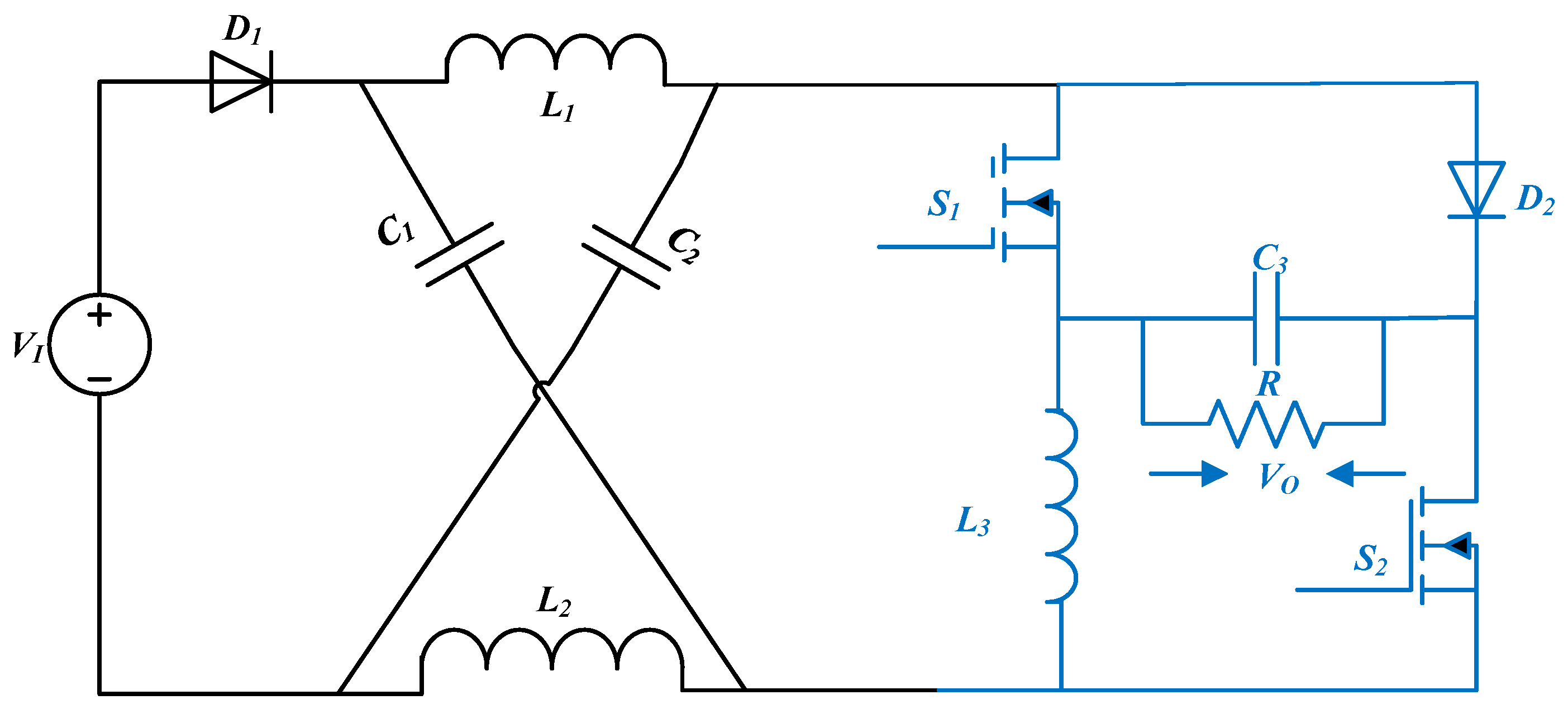
2. Circuit Configuration and Operating Principle of the Proposed HS-SZC
2.1. The Configuration of the Proposed HS-SZC
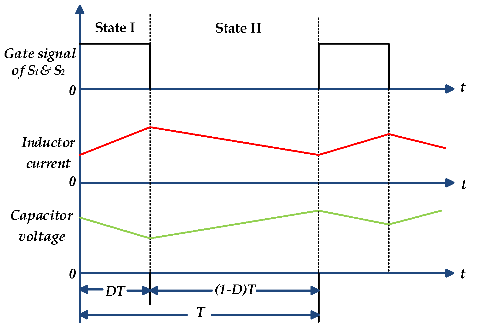
2.2. Operating Principle of the HS-SZC
- Power components are assumed as ideal without having turn-on resistances and voltage drops;
- Large capacitors are used in order to ignore voltage ripples;
- The proposed converter is operating in the CCM.
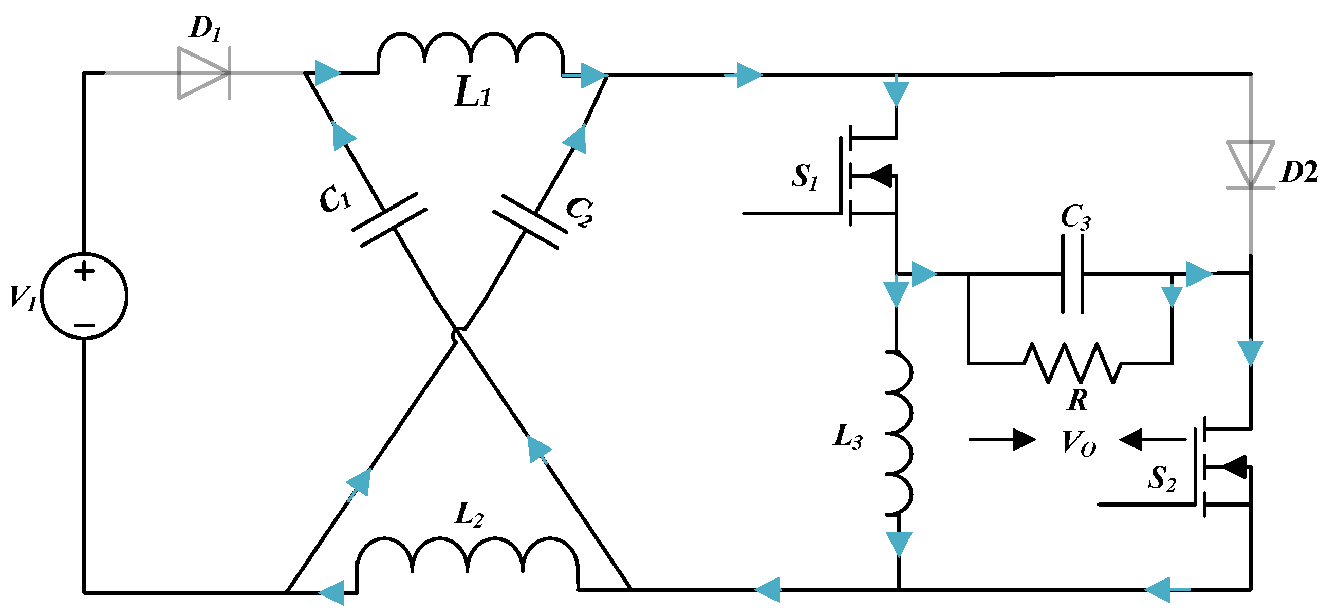
2.2.1. Mode 1
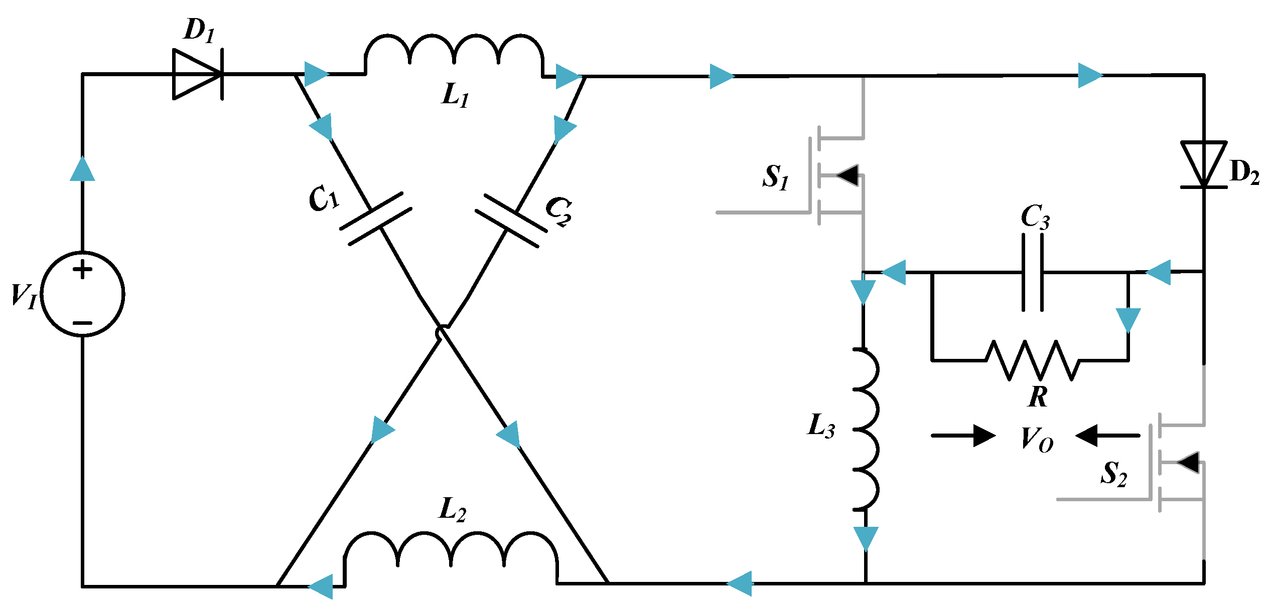
2.2.2. Mode 2
3. Calculation of Current Stresses
4. Component Design Principle
4.1. Inductor Design
4.2. Capacitor Design
4.3. Switch and Diode Design
5. Analysis of the Proposed HS-SZC with Non-Ideal Elements
5.1. Impact of Non-Ideal Elements on the Output Voltage
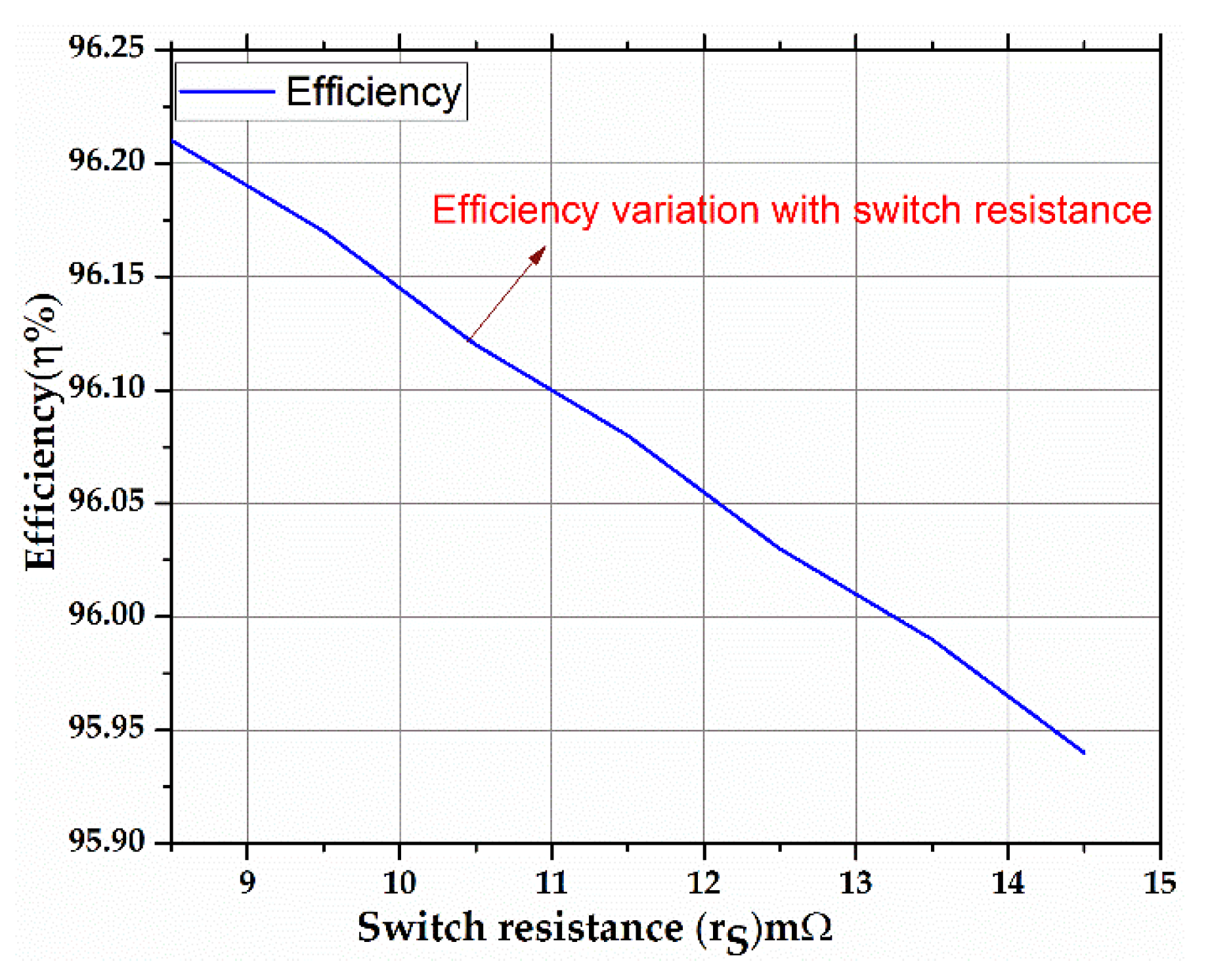
5.2. Impact of Non-Ideal Elements on the Efficiency
5.2.1. Power Losses in the Switch
5.2.2. Power Losses in the Diode
5.2.3. Power Losses in the Inductor
5.2.4. Power Losses in the Capacitor
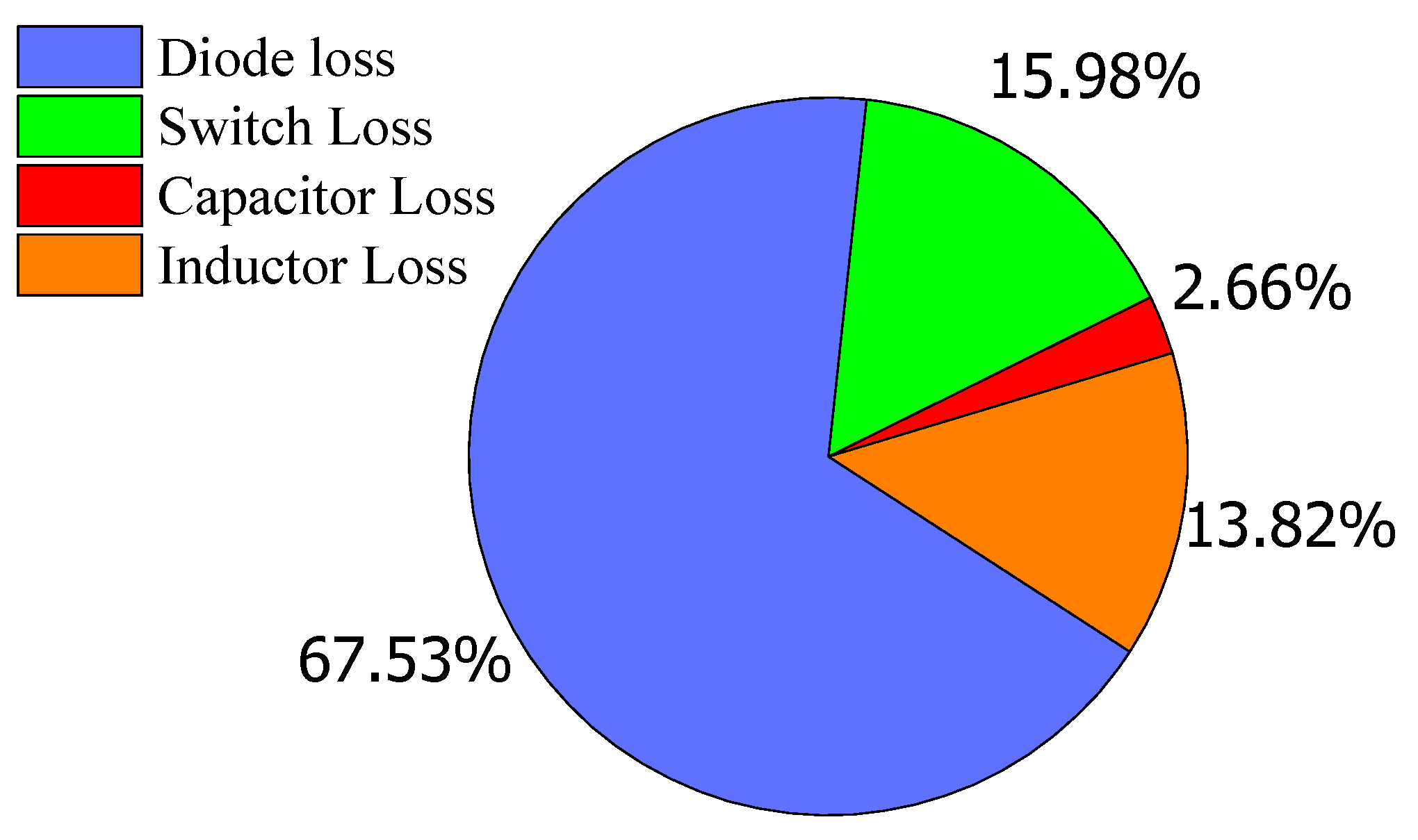
5.2.5. Total Power Losses
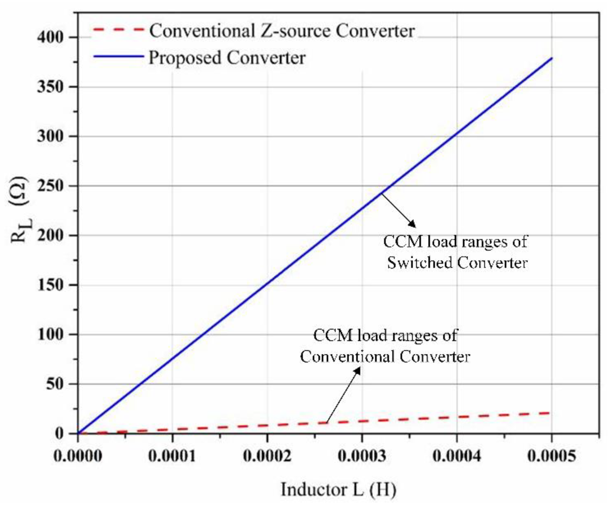
6. Conditions for the CCM Operation and Load Range of the Proposed Converter
7. Comparative Analysis of the Proposed Converter
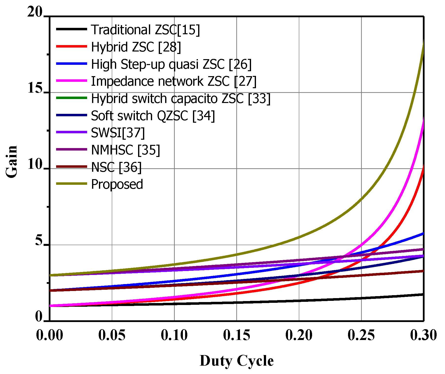
7.1. Comparison in Terms of the Boost Ability
7.2. Comparison in Terms of the Number of Components
7.3. Comparison in Terms of Voltage Stress
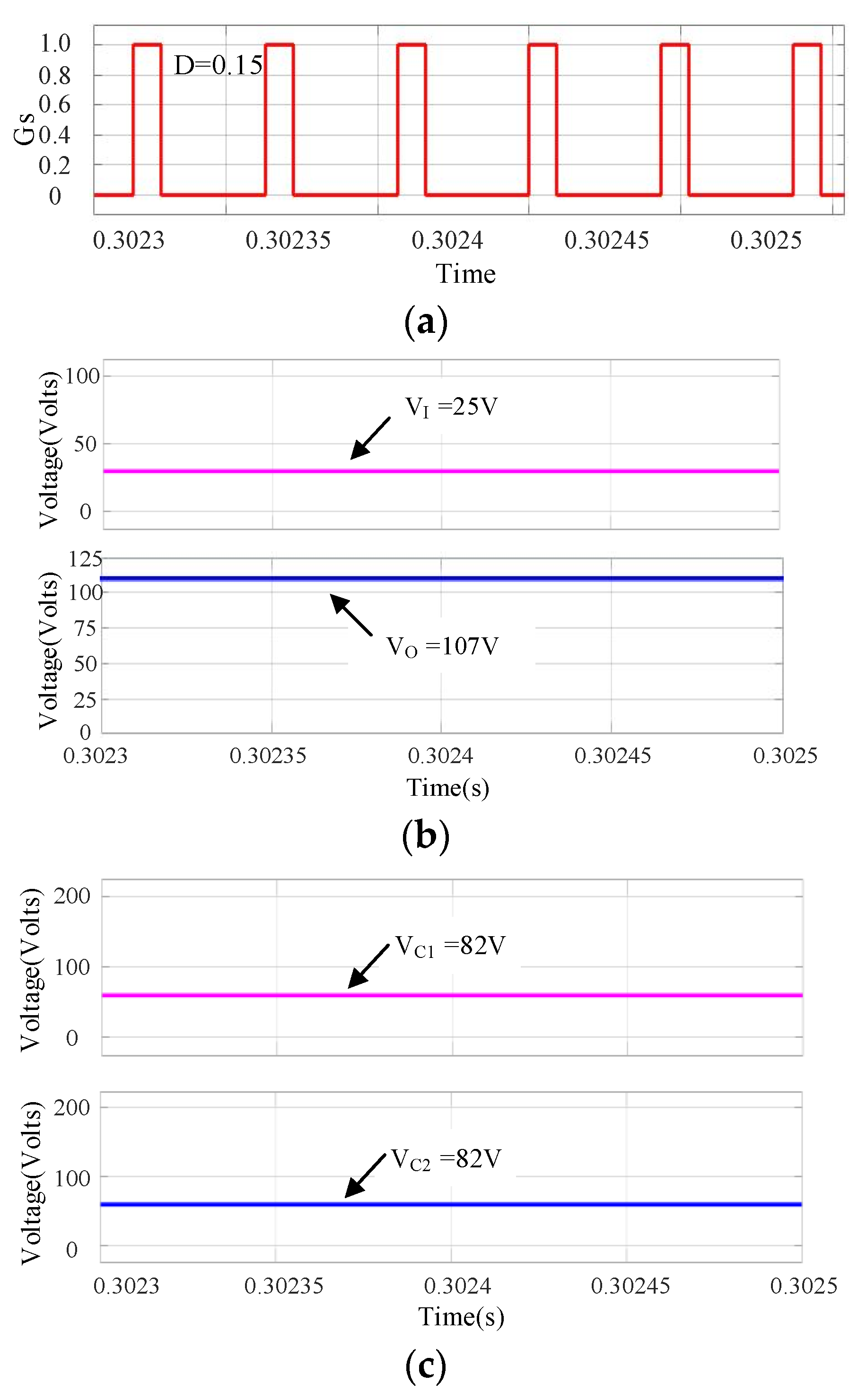
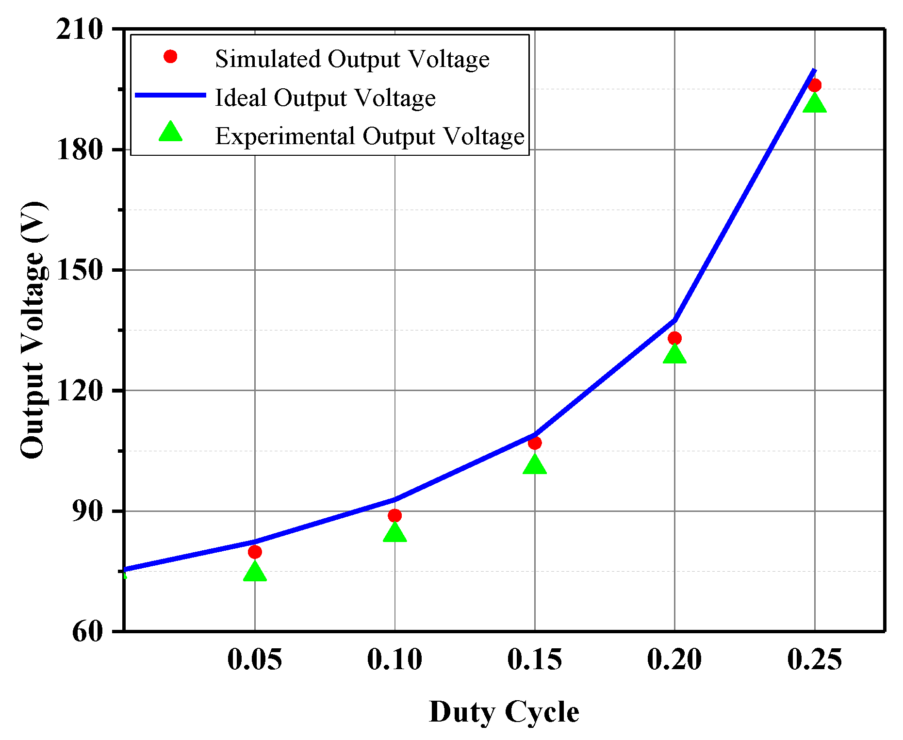
8. Simulation Results
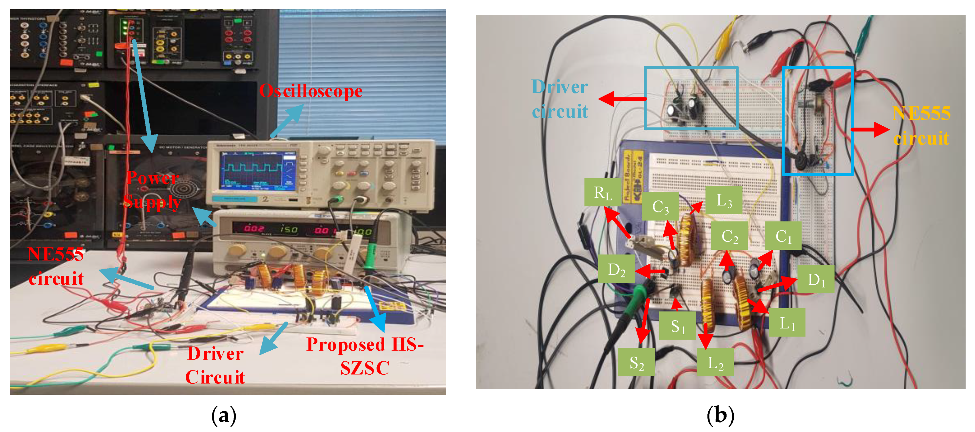
9. Experimental Results
10. Conclusions and Future Research
Author Contributions
Funding
Data Availability Statement
Acknowledgments
Conflicts of Interest
References
- Gira, N.; Dahiya, A.K. Solar PV-BES in distribution system with novel technique for DC voltage regulation. Eng. Sci. Technol. Int. J. 2020, 23, 1058–1067. [Google Scholar] [CrossRef]
- Ahmed, T.A.; Mohamed, E.E.; Youssef, A.-R.; Ibrahim, A.; Saeed, M.S.; Ali, A.I. Three phase modular multilevel inverter-based multi-terminal asymmetrical DC inputs for renewable energy applications. Eng. Sci. Technol. Int. J. 2020, 23, 831–839. [Google Scholar] [CrossRef]
- Chen, Y.; Member, S.; Huang, A.Q.; Yu, X.; Member, S. A High Step-Up Three-Port DC—DC Converter for Stand-Alone PV/Battery Power Systems. IEEE Trans. Power Electron. 2013, 28, 5049–5062. [Google Scholar] [CrossRef]
- Gu, B.; Dominic, J.; Lai, J.-S.; Zhao, Z.; Liu, C. High Boost Ratio Hybrid Transformer DC—DC Converter for Photovoltaic Module Applications. IEEE Trans. Power Electron. 2012, 28, 2048–2058. [Google Scholar] [CrossRef]
- Zubieta, L.E.; Lehn, P.W. A High Efficiency Unidirectional DC/DC Converter for Integrating Distributed Resources into DC Microgrids. In Proceedings of the IEEE First International Conference on DC Microgrids (ICDCM), Atlanta, GA, USA, 7–10 June 2015; pp. 280–284. [Google Scholar]
- Syam, M.S.; Kailas, T.S. Grid connected PV system using Cuk converter. In Proceedings of the 2013 Annual International Conference on Emerging Research Areas and 2013 International Conference on Microelectronics, Communications and Renewable Energy, Kanjirapally, India, 4–6 June 2013. [Google Scholar] [CrossRef]
- Sener, E.; Ertasgin, G. A 3-ph Grid-Connected Photovoltaic Inverter Utilizing Super-Lift Luo Converter. In Proceedings of the 2018 2nd International Symposium on Multidisciplinary Studies and Innovative Technologies (ISMSIT), Ankara, Turkey, 19–21 October 2018; pp. 1–5. [Google Scholar] [CrossRef]
- Saravanan, S.; Babu, N.R. Analysis and implementation of high step-up DC-DC converter for PV based grid application. Appl. Energy 2017, 190, 64–72. [Google Scholar] [CrossRef]
- Padmanaban, S.; Kabalci, E.; Iqbal, A.; Abu-Rub, H.; Ojo, O. Control strategy and hardware implementation for DC-DC boost power circuit based on proportional–integral compensator for high voltage application. Eng. Sci. Technol. Int. J. 2015, 18, 163–170. [Google Scholar] [CrossRef] [Green Version]
- Shahir, F.M.; Babaei, E.; Farsadi, M. Voltage-Lift Technique Based Nonisolated Boost DC-DC Converter: Analysis and Design. IEEE Trans. Power Electron. 2017, 33, 5917–5926. [Google Scholar] [CrossRef]
- Hu, X.; Gong, C. A High Gain Input-Parallel Output-Series DC/DC Converter with Dual Coupled Inductors. IEEE Trans. Power Electron. 2015, 30, 1306–1317. [Google Scholar] [CrossRef]
- Salehi, S.; Zahedi, N.; Kheirollahi, R.; Babaei, E. Ultra High Step-up DC-DC Converter Based on Switched Inductor-Capacitor Cells. In Proceedings of the 2019 10th International Power Electronics, Drive Systems and Technologies Conference (PEDSTC), Shiraz, Iran, 12–14 February 2019; pp. 367–372. [Google Scholar] [CrossRef]
- Tang, Y.; Fu, D.; Wang, T.; Xu, Z. Hybrid Switched-Inductor Converters for High Step-Up Conversion. IEEE Trans. Ind. Electron. 2015, 62, 1480–1490. [Google Scholar] [CrossRef]
- Prudente, M.; Pfitscher, L.L.; Emmendoerfer, G.; Romaneli, E.F.; Gules, R. Voltage Multiplier Cells Applied to Non-Isolated DC-DC Converters. IEEE Trans. Power Electron. 2008, 23, 871–887. [Google Scholar] [CrossRef]
- Fang, X. A novel Z-source dc-dc converter. In Proceedings of the 2008 IEEE International Conference on Industrial Technology, Chengdu, China, 21–24 April 2008; pp. 8–11. [Google Scholar] [CrossRef]
- Galigekere, V.P.; Kazimierczuk, M.K. Analysis of PWM Z-Source DC-DC Converter in CCM for Steady State. IEEE Trans. Circuits Syst. I Regul. Pap. 2012, 59, 854–863. [Google Scholar] [CrossRef]
- Takiguchi, T.; Koizumi, H. Quasi-Z-source dc-dc converter with voltage-lift technique. In Proceedings of the IECON 2013 - 39th Annual Conference of the IEEE Industrial Electronics Society, Vienna, Austria, 10–13 November 2013; pp. 1191–1196. [Google Scholar] [CrossRef]
- Yang, L. A Quasi-Z -Source DC-DC Converter. In Proceedings of the 2014 IEEE Energy Conversion Congress and Exposition (ECCE), Pittsburgh, PA, USA, 14–18 September 2014. [Google Scholar] [CrossRef]
- Qiaojie, Z.; Yunxia, L.; Qiao, Y. Quasi-Z-source DC/DC converter based on switched inductor-capacitor unit and passivity based controller. In Proceedings of the 8th Renewable Power Generation Conference (RPG 2019), Shanghai, China, 24–25 October 2019; pp. 1–7. [Google Scholar] [CrossRef]
- Evran, F.; Aydemir, M.T. Z-source-based isolated high step-up converter. IET Power Electron. 2013, 6, 117–124. [Google Scholar] [CrossRef]
- Sharifi, S.; Monfared, M. Modified Series and Tapped Switched-Coupled-Inductors Quasi-Z-Source Networks. IEEE Trans. Ind. Electron. 2019, 66, 5970–5978. [Google Scholar] [CrossRef]
- Poorali, B.; Torkan, A.; Adib, E. High step-up Z-source DC-DC converter with coupled inductors and switched capacitor cell. IET Power Electron. 2015, 8, 1394–1402. [Google Scholar] [CrossRef]
- Zhang, G.; Zhang, B.; Li, Z.; Qiu, D.; Yang, L.; Halang, W.A. A 3-Z-Network Boost Converter. IEEE Trans. Ind. Electron. 2015, 62, 278–288. [Google Scholar] [CrossRef]
- Torkan, A.; Ehsani, M. A Novel Nonisolated Z-Source DC-DC Converter for Photovoltaic Applications. IEEE Trans. Ind. Appl. 2018, 54, 4574–4583. [Google Scholar] [CrossRef]
- Krishna, M.V.; Varma, L.T.V.; Kumar, M.A. Simulation of High Step up Z-Source DC-DC Converter with Voltage Multiplier Using Coupled Inductors. IJRAR Int. J. Res. Anal. Rev. 2018, 5, 594–598. [Google Scholar]
- Haji-Esmaeili, M.M.; Babaei, E.; Sabahi, M. High Step-Up Quasi-Z Source DC-DC Converter. IEEE Trans. Power Electron. 2018, 33, 10563–10571. [Google Scholar] [CrossRef]
- Zhang, G.; Iu, H.H.-C.; Zhang, B.; Li, Z.; Fernando, T.; Chen, S.-Z.; Zhang, Y. An Impedance Network Boost Converter with a High-Voltage Gain. IEEE Trans. Power Electron. 2017, 32, 6661–6665. [Google Scholar] [CrossRef]
- Shen, H.; Zhang, B.; Qiu, D. Hybrid Z-Source Boost DC-DC Converters. IEEE Trans. Ind. Electron. 2017, 64, 310–319. [Google Scholar] [CrossRef]
- Vaz, A.R.; Tofoli, F.L. Detailed design procedure of a DC-DC buck-boost converter employing a passive snubber. In Proceedings of the 2017 Brazilian Power Electronics Conference (COBEP), Juiz de Fora, Brazil, 19–22 November 2017; pp. 1–6. [Google Scholar] [CrossRef]
- H. P. International R. Mosfet. IRFP4768PbF. p. PD-97379. Available online: https://www.infineon.com/dgdl/irfp4768pbf.pdf?fileId=5546d462533600a40153562c959b2021 (accessed on 12 December 2016).
- Zeng, J.; Wu, J.; Liu, J.; Guo, H. A Quasi-Resonant Switched-Capacitor Multilevel Inverter with Self-Voltage Balancing for Single-Phase High-Frequency AC Microgrids. IEEE Trans. Ind. Inform. 2017, 13, 2669–2679. [Google Scholar] [CrossRef]
- Yang, L.; Qiu, D.; Zhang, B.; Zhang, G.; Xiao, W. A modified Z-source DC-DC converter. In Proceedings of the 2014 16th European Conference on Power Electronics and Applications, Lappeenranta, Finland, 26–28 August 2014. [Google Scholar] [CrossRef]
- Zhang, Y.; Liu, Q.; Gao, Y.; Li, J.; Sumner, M. Hybrid Switched-Capacitor/Switched-Quasi-Z-Source Bidirectional DC-DC Converter with a Wide Voltage Gain Range for Hybrid Energy Sources EVs. IEEE Trans. Ind. Electron. 2019, 66, 2680–2690. [Google Scholar] [CrossRef]
- Quasi-z-source, S.H.S.; Converter, D.C.D.C. Soft-Switched High Step-Up Quasi-Z-Source DC-DC Converter. IEEE Trans. Ind. Electron. 2020, 67, 4547–4555. [Google Scholar]
- Maalandish, M.; Hosseini, S.H.; Ghasemzadeh, S.; Babaei, E.; Jalilzadeh, T. A Novel Multiphase High Step-Up DC/DC Boost Converter with Lower Losses on Semiconductors. IEEE J. Emerg. Sel. Top. Power Electron. 2019, 7, 541–554. [Google Scholar] [CrossRef]
- Wu, G.; Ruan, X.; Ye, Z. Nonisolated High Step-Up DC—DC Converters. IEEE Trans. Ind. Electron. 2015, 62, 383–393. [Google Scholar] [CrossRef]
- Chen, M.; Li, K.; Hu, J.; Ioinovici, A. Generation of a Family of Very High DC Gain Power Electronics Circuits Based on Switched-Capacitor-Inductor Cells Starting from a Simple Graph. IEEE Trans. Circuits Syst. I Regul. Pap. 2016, 63, 2381–2392. [Google Scholar] [CrossRef]


| Parameters | Component Stress | Parameters | Component Stress |
|---|---|---|---|
| Output voltage (VO) | Input current (II) | ||
| Voltage stresses on capacitors (VC1) and (VC2) | Current stresses on inductors (IL1) and (IL2) | ||
| Voltage stresses on switches (VS1) and (VS2) | Current stresses on switches (IS1) and (IS2) | ||
| Current stress on diode (D1) | Current stress on diode (D2) |
| Parameters | Symbol | Value | Parameters | Symbol | Value |
|---|---|---|---|---|---|
| Duty cycle | D | 0.20 | Inductor resistance | rL | 0–30 mΩ |
| Input voltage | VI | 40 V | Capacitor resistance | rC | 10 mΩ |
| Inductor current | IL | 5 A | Switching frequency | fS | 25 kHz |
| Voltage drop | VD | 0–1.5 V | Switch resistance | rS | 8.5–14.5 mΩ |
| Ref. | Components | Gain Factor | Features and Drawbacks |
|---|---|---|---|
| [15] | 2 Inductors 3 Capacitors 1 Switch 2 Diodes | ✓Suitable for solving shoot-through problems × Low boost factor | |
| [8] | 3 Inductors 5 Capacitors 1 Switch 3 Diodes | ✓Utilizing smaller duty cycle for higher gain ✓Higher boost factor × The different ground for input and output × Utilize a higher number of components | |
| [9] | 3 Inductors 7 Capacitors 1 Switch 5 Diodes | ✓can attend high gain by adding an extra stage ✓low voltage stresses on components ×The different ground for input and output × Utilize a higher number of components | |
| [10] | 4 Inductors 3 Capacitors 1 Switch 8 Diodes | ✓Utilizing smaller duty cycle for higher gain × Utilize a higher number of components | |
| [11] | 2 Inductors 6 Capacitors 5 Switches 5 Diodes | ✓Wide range of voltage gain × Utilize a higher number of components | |
| [12] | 5 Inductors 6 Capacitors 2 Switches 2 Diodes | ✓ Reduced diode conduction loss ✓common ground between input and output × Utilize higher number of components | |
| [13] | 2 Switches 6 Diodes (j = k = 1) 2 Inductors 4 Capacitors | ✓ Low voltage stress on components ✓ High voltage gain × Utilize higher number of components. | |
| [36] | 1 Switch 4 Diodes 2 Inductors 5 Capacitors | ✓Increased voltage gain × Utilize higher number of components | |
| [37] | 1 Switch 5 Diodes 1 Inductor 5 Capacitors | ✓ Low voltage stress on components ✓Common ground × Higher parts count. | |
| Proposed converter | 3 Inductors 3 Capacitors 2 Switches 2 Diodes | ✓Utilizing smaller duty cycle for higher gain ✓Higher boost factor ✓ Utilize a lower number of components ✓ Reduced power loss × The different ground for input and output |
| Parameters | Symbol | Value | Parameters | Symbol | Value |
|---|---|---|---|---|---|
| Duty cycle | D | 0.15 | Inductor resistance | rL | 0–30 mΩ |
| Input voltage | VI | 25 V | Capacitor resistance | rC | 10 mΩ |
| Inductors | L1-3 | 380 µH | Switching frequency | fS | 20 kHz |
| Capacitors | C1-3 | 330 µF | Switch resistance | rS | 12.5 mΩ |
| Device | Specification |
|---|---|
| Inductors | 380 µH/10 A |
| Capacitors | 330 µF/100 V |
| Diode | MIC 10a10 |
| MOSFET | IRF540 |
| Signal generator | NE555P |
| MOSFET driver IC | IR2117 |
Publisher’s Note: MDPI stays neutral with regard to jurisdictional claims in published maps and institutional affiliations. |
© 2021 by the authors. Licensee MDPI, Basel, Switzerland. This article is an open access article distributed under the terms and conditions of the Creative Commons Attribution (CC BY) license (https://creativecommons.org/licenses/by/4.0/).
Share and Cite
Kumar, R.; Kannan, R.; Nor, N.B.M.; Mahmud, A. A High Step-Up Switched Z-Source Converter (HS-SZC) with Minimal Components Count for Enhancing Voltage Gain. Electronics 2021, 10, 924. https://doi.org/10.3390/electronics10080924
Kumar R, Kannan R, Nor NBM, Mahmud A. A High Step-Up Switched Z-Source Converter (HS-SZC) with Minimal Components Count for Enhancing Voltage Gain. Electronics. 2021; 10(8):924. https://doi.org/10.3390/electronics10080924
Chicago/Turabian StyleKumar, Rahul, Ramani Kannan, Nursyarizal Bin Mohd Nor, and Apel Mahmud. 2021. "A High Step-Up Switched Z-Source Converter (HS-SZC) with Minimal Components Count for Enhancing Voltage Gain" Electronics 10, no. 8: 924. https://doi.org/10.3390/electronics10080924