Abstract
This paper deals with a single-stage single-ended inverter-based Operational Transconductance Amplifiers (OTA) with improved composite transistors for ultra-low-voltage supplies, while maintaining a small-area, high power-efficiency and low output signal distortion. The improved composite transistor is a combination of the conventional composite transistor and forward-body-biasing to further increase voltage gain. The impact of the proposed technique on performance is demonstrated through post-layout simulations referring to the TSMC 180 nm technology process. The proposed OTA achieves 54 dB differential voltage gain, 210 Hz gain–bandwidth product for a 10 pF capacitive load, with a power consumption of 273 pW with a 0.3 V power supply, and occupies an area of 1026 μm2. For a 0.6 V voltage supply, the proposed OTA improves its voltage gain to 73 dB, and achieves a 15 kHz gain–bandwidth product with a power consumption of 41 nW.
1. Introduction
The development of electronic devices that are increasingly less dependent on battery charging requires Integrated Circuits (ICs) able to operate with Ultra-Low-Voltage (ULV) supply with an Ultra-Low-Power (ULP) consumption. A recent approach to address this request relies on digital-based and supply-voltage scalable ICs [1,2,3,4,5,6,7,8,9]. In this framework, the design of ULV Operational Transconductance Amplifiers (OTA) with appreciable performance (i.e., rail-to-rail input/output voltage swing and high transconductance–gain independent of process, supply voltage, and temperature variations [10]) becomes more and more challenging.
Inverter-based OTA topologies [11,12] and their respective ULV variations [13,14] have been proposed, as well as push–pull-based, bulk-driven OTAs [15,16,17,18]. An improved single-ended OTA has been proposed in [19], exploiting the properties of improved composite transistors [20] into a variation of the bulk Nauta inverter-based OTA [21]. This approach improves the voltage gain for a single-stage amplifier but shows a limited input voltage swing.
This work further exploits the improved composite transistors of inverters [19] into a single-ended version of the fully differential OTA in [14]. This results in an enhanced voltage gain, a higher linearity and a lower power consumption at the minimum supply voltages.
In Section 2, the improved composite transistor technique is briefly reviewed. Then, in Section 3, the employed self-biased inverter with the forward body bias is described. Based on this, in Section 4, the proposed inverter-based OTA is described. In Section 5, the characteristics of the proposed OTA are then verified and compared through post-layout simulations with similar circuits designed in the 180 nm technology process. Finally, in Section 6, conclusions are drawn.
2. Composite Transistor Forward-Body-Biasing Analysis
Figure 1 represents an N-type improved composite transistor. It consists of a series connection of two independently forward-body-biased N-type Metal-Oxide Semiconductor (MOS) transistors MN1 and MN2, as first proposed in [20] and described in detail in [19], by using the Unified Current Control Model (UICM) all-region transistor model [22].
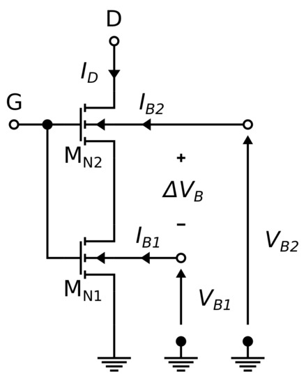
Figure 1.
Improved composite transistor.
Considering that , operates in the linear region, operates in the saturation region, and both transistors operate in weak inversion, the improved composite transistor drain current can be calculated as follows:
where
is the sheet normalization current, and are, respectively, the transistor gate and bulk terminal voltages referenced to the ground, is the threshold voltage, n is the slope factor, is the thermal voltage, is the charge mobility, and is the gate oxide capacitance per area.
The improved composite transistor equivalent aspect ratio is defined as:
where
represents a correction factor for the current drain definition due to the difference between the body-bias of the series transistors MN2 and MN1, assuming the transistors are operating in weak inversion, and
is the ratio between transistors MN1 and MN2 physical aspect ratios and .
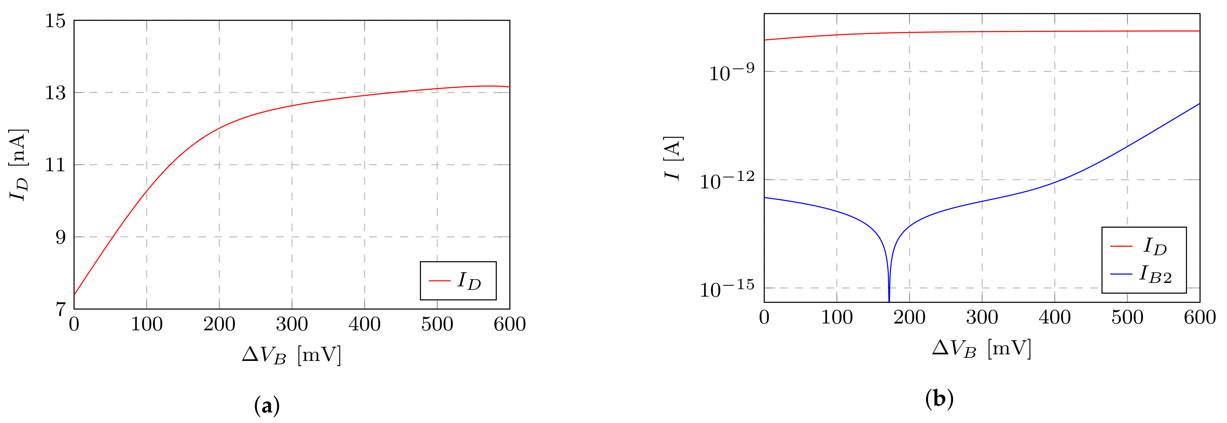
Figure 2a shows how the drain current increases with for equally sized transistors with 1.26 um width and 0.42 length, in the TSMC 180 nm Complementary Metal-Oxide Semiconductor (CMOS) technology process, operating at 27 C, for mV, V, , and ranging from 0 to 600 mV. Figure 2b shows how the parasitic substrate current increases with . When is approximately 170 mV, is almost zero, as is almost equal to the transistor MN2 source terminal voltage. For voltages higher than 170 mV, MN2 is forward-body-biased and increases exponentially for voltages higher than 400 mV.
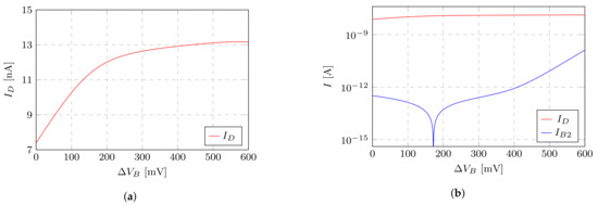
Figure 2.
Improved composite transistor simulation results for VG = VD = 300 mV, VB1 = 0.0 V and 0 ≤ VB2 ≤ 600 mV: (a) drain current ID on y-axis nA range versus ∆VB = VB2 − VB1; and (b) drain current ID and the parasitic substrate current IB2 versus ∆VB = VB2 − VB1.
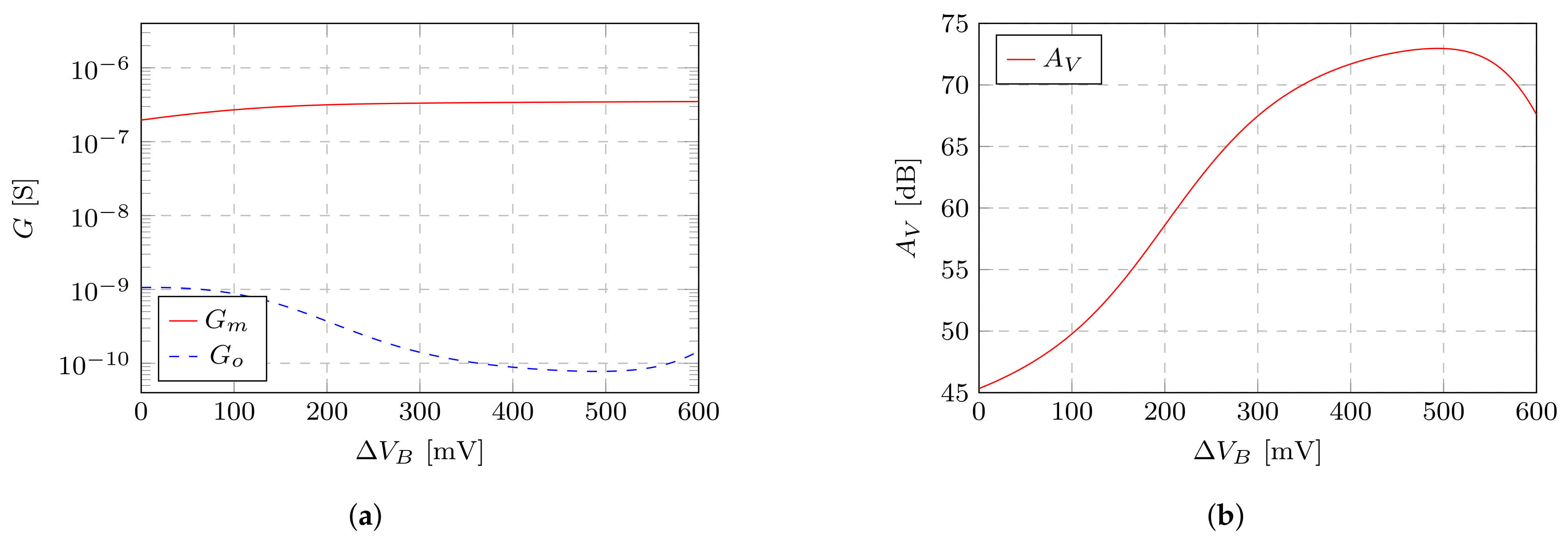
Referring to the same specification, Figure 3a shows the improved composite transistor transconductance = () and output conductance = (), and Figure 3b shows its intrinsic voltage gain , which is the ratio between and . Figure 3b shows how increases exponentially with till mV. Then, increases with a reduced slope until it reaches its peak at mV. In particular, is increased by an order of magnitude (20 dB) for mV and almost two orders of magnitude (38 dB) for mV.
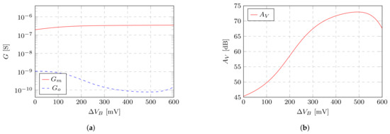
Figure 3.
Improved composite transistor simulation results for VG = VD = 0.3 V, VB1 = 0.0 V and 0 ≤ VB2 ≤ 0.6 V: (a) transconductance Gm and output conductance Go versus ∆VB = VB2 − VB1; and (b) intrinsic voltage gain AV versus ∆VB = VB2 − VB1.
3. Proposed Inverter Made of Composite Transistors with Forward-Body-Bias
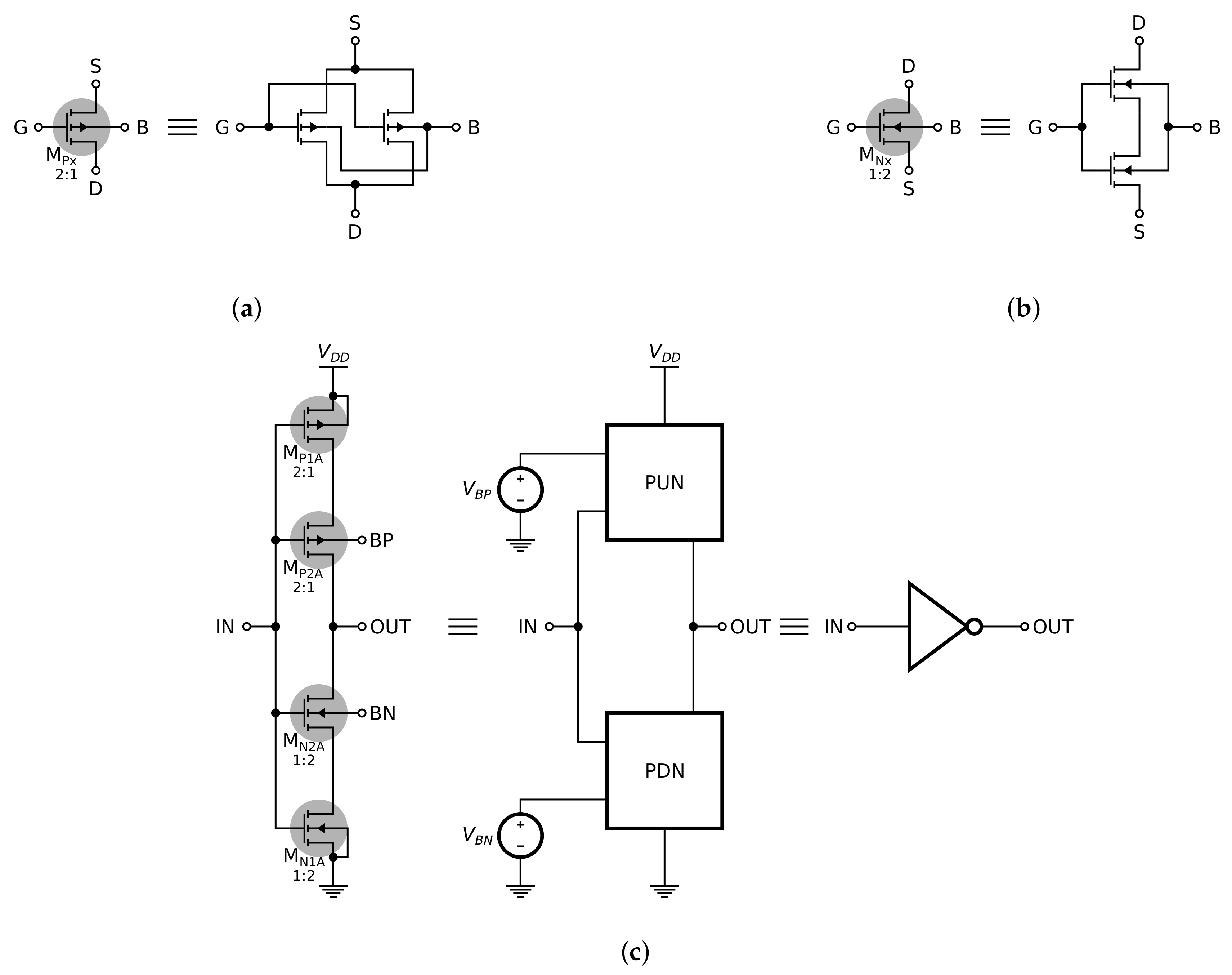
Figure 4a,b shows, respectively, N-type and P-type rectangular transistor arrays [23,24] MNxA and MPxA. The PMOS devices are 2:1 parallel arrays (two single P-MOS transistors of size in parallel), whereas the NMOS devices are 1:2 series arrays (two single N-MOS transistors of size in series). Both NMOS and PMOS single transistors that build each N-type and P-type transistor array have identical width and lengths and aspect ratios, but the PMOS equivalent transistors have an aspect ratio four times larger than the NMOS equivalent transistors in order to balance the PMOS pull-up and NMOS pull-down networks. The same ratio between pull-up and pull-down networks could be achieved by using a single PMOS transistor with channel widths four times larger than the single NMOS transistors channel width while keeping the transistor length identical, but this would increase the inverter total active area by 25%.
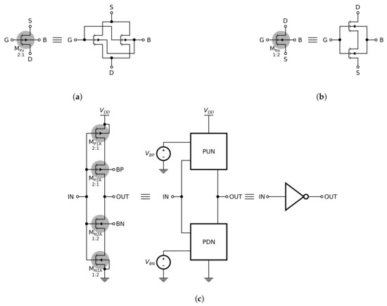
Figure 4.
Transistors arrays: (a) P-type 2:1 parallel transistor array and; (b) N-type 1:2 series transistor array; (c) transistor level schematic of the proposed inverter made of composite transistors with forward-body-bias and equivalent representations as an inverter.
The improved composite transistor can be represented as single transistors with an equivalent aspect ratio as in (3).
Two N-type and 2 P-type transistor arrays, respectively, MP1A, MN2A and MP1A, MP2A, are placed in series as in Figure 4c to build an inverter.
The inverter small-signal voltage gain is equal to the ratio between an equivalent inverter transconductance and output conductance .
These and are, respectively, functions of the PMOS and NMOS equivalent transistors gate-drain small-signal transconductance and drain conductance , as derived from Equations (7) and (8), accordingly to the UICM model approximation to the transistor weak inversion operation [22]. These small-signal parameters are a function of the quiescent current [21] (also known as short-circuit current), slope factor n, the thermal voltage and the early voltage .
Therefore, the inverter small-signal voltage gain can be rewritten as:
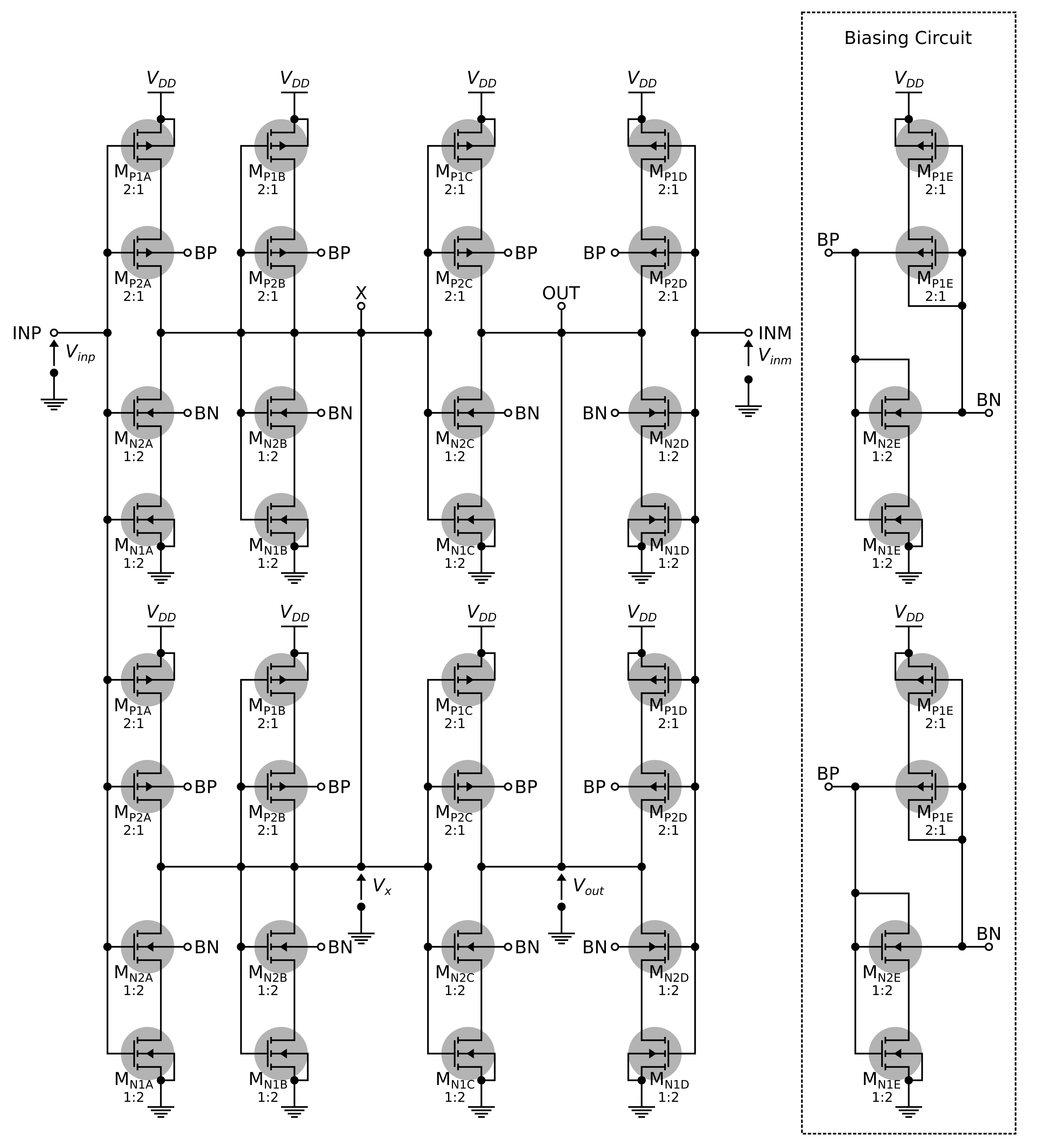
This schematic in Figure 4c can be equivalently translated into a pull-up and pull-down network (respectively, PUN and PDN) of an inverter biased by two additional voltages and . This represents an equivalent inverter made of composite transistors with a forward-body-bias. Such an inverter is the building block of the proposed inverter-based OTA described in this paper.
4. Proposed Operational Transconductance Amplifier
Differential inverter-based OTAs can use positive feedback and active load [11,13], or forward common-mode cancellation [12,14], to attenuate common-mode signals, as shown in Figure 5.
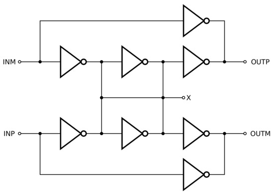
Figure 5.
Fully-differential inverter-based Operational Transconductance Amplifier (OTA) with forward common-mode cancellation [12].

Figure 6.
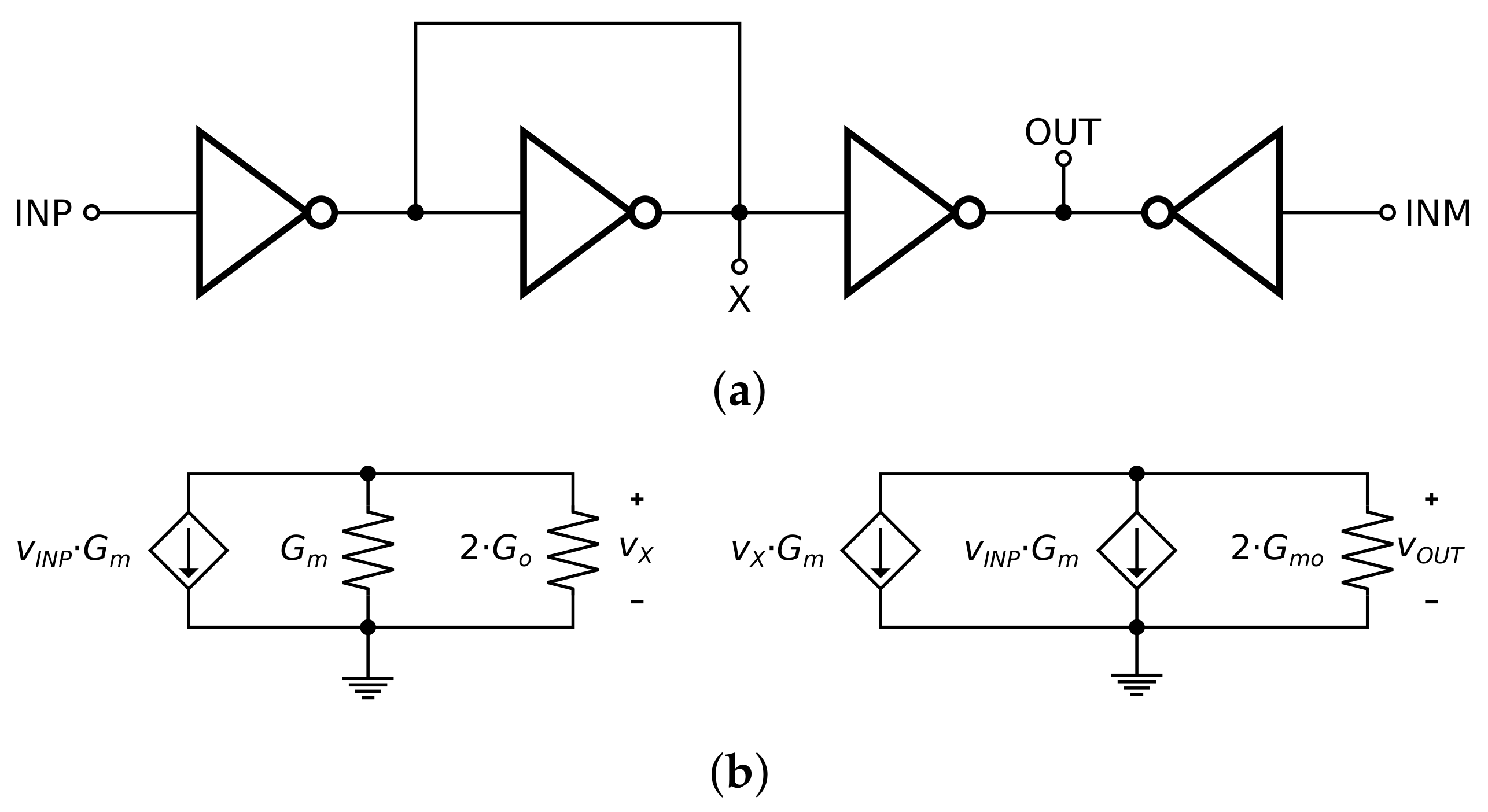
Single-ended inverter-based OTA: (a) simplified schematic, and (b) respective small-signal representation.
The small-signal circuit of this OTA is shown in Figure 6b, where the corresponding transconductance and output conductance are represented as and , and its unloaded low frequency voltage gain can be modeled as , as described in Equation (8).
The small-signal differential output voltage at very low frequencies can be expressed as
Considering that , the small-signal differential voltage gain can be derived as
and, considering that , the common-mode voltage gain can be derived as
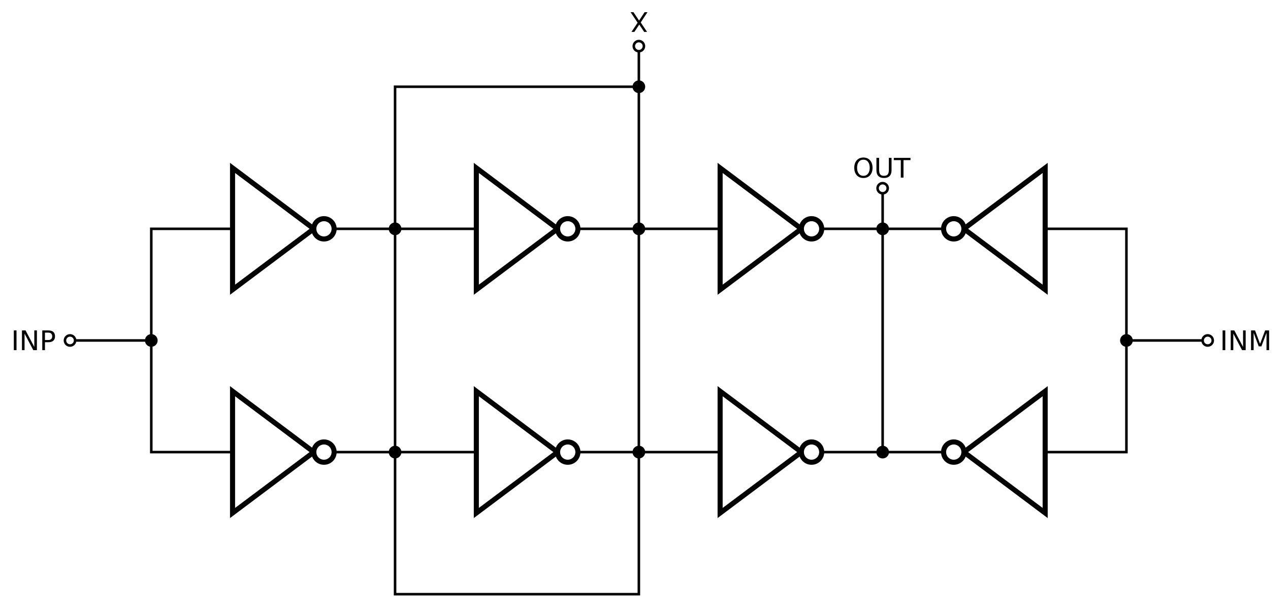
Figure 7 shows the proposed inverter-based OTA, which is equivalent to the OTA shown in Figure 6a, but the former has two inverters in parallel for each one represented in the latter. All inverters are identical and made of improved composite transistors. By doubling each inverter, the common-centroid technique can be used to design this OTA layout. Furthermore, by using N inverters in parallel, the OTA transconductance is multiplied by N, and both mismatch and noise are reduced by . Obviously, power consumption and area also multiplied by N. Since the OTA output conductance is also multiplied, the OTA voltage gain remains the same.
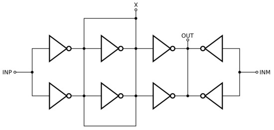
Figure 7.
Proposed single-ended, inverter-based OTA with improved composite transistor circuit schematic.
Figure 8 shows the transistor-level proposed OTA schematic. As shown in Figure 3b, the intrinsic voltage gain can be increased by means of the two bulk terminals of the composite transistor. The higher their voltage difference , the higher the intrinsic voltage gain . Therefore, in order to maximize with no additional supply voltages, the transistors pull-down networks are connected to the ground or to the supply voltage . In particular, bulk terminals of the transistors MN1A-D are connected to the ground, whereas those of the transistors MN2A-D are tied to the node BN, which is connected indirectly to the supply voltage . In fact, BN is connected to the drain of transistor MP2E and both transistors MP1E and MP2E are pseudo-resistors with very large resistances. Thus, if the substrate parasitic current increases, the pseudo-resistor voltage drop increases and limits it to relatively insignificant levels [21,25]. Notice that for FD-SOI process technologies [26], those transistors would not be necessary because there is no parasitic substrate current. Symmetrically, the same body-bias is applied to the pull-up network referring to the BP node.
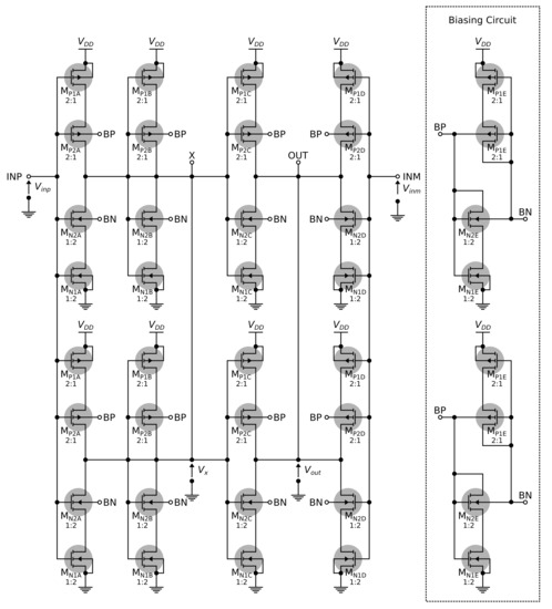
Figure 8.
Proposed single-ended inverter-based OTA transistor-level circuit schematic.
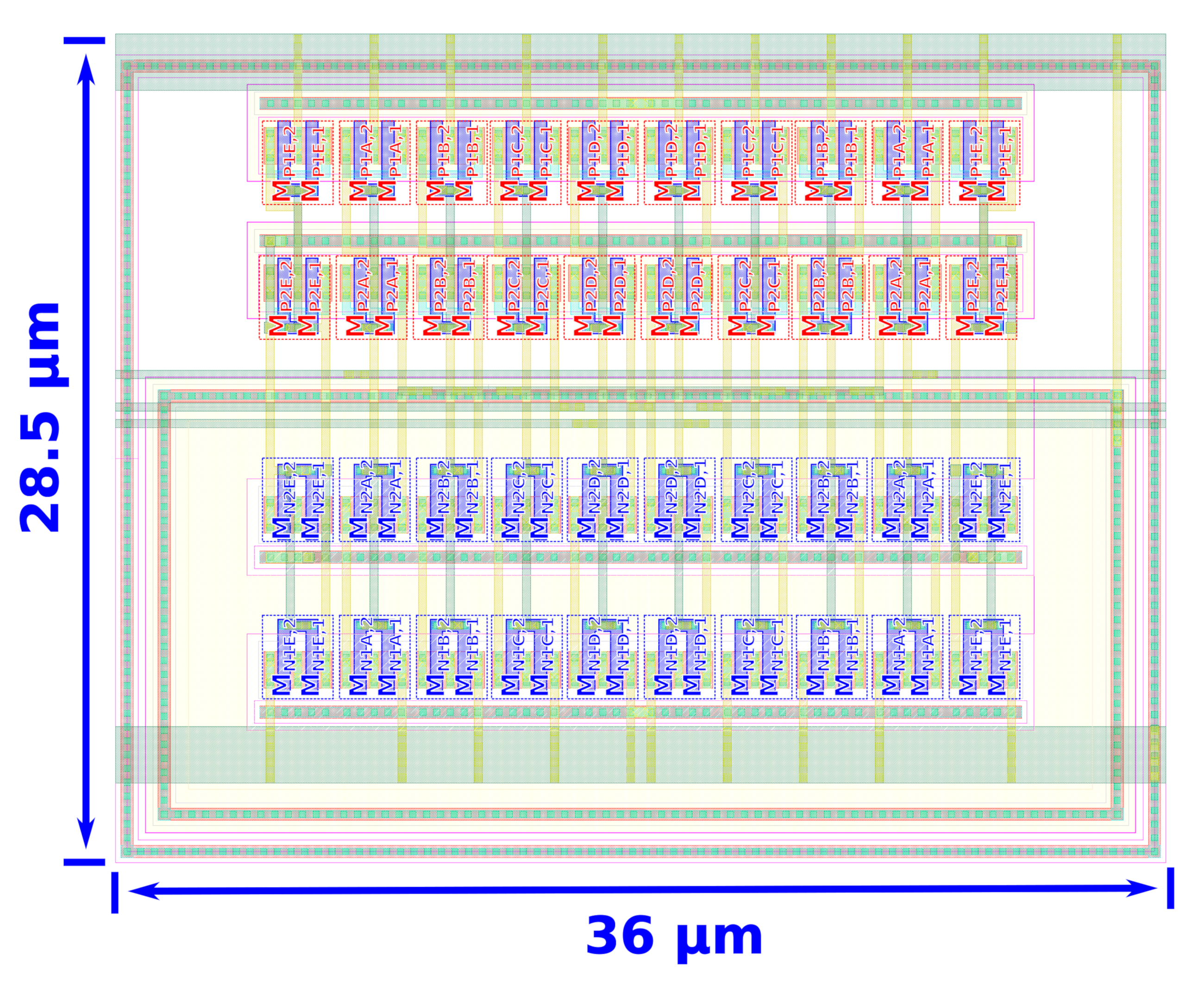
Figure 9 shows the proposed OTA layout. The width W of each unit transistor is set on the basis of the minimum sizing requirement of the isolated n-well and p-well.
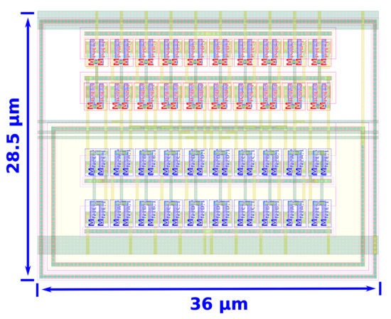
Figure 9.
Layout view of the proposed inverter-based operation transconductance amplifier.
Based on this, all the unit transistors, both PMOS and NMOS have an identical aspect ratio equal to
All inverters are doubled in order to use the common-centroid layout technique. The transistors located at the edge of the layouts are the pseudo-resistors used to limit the substrate current and also function as dummies.
5. Simulation Results
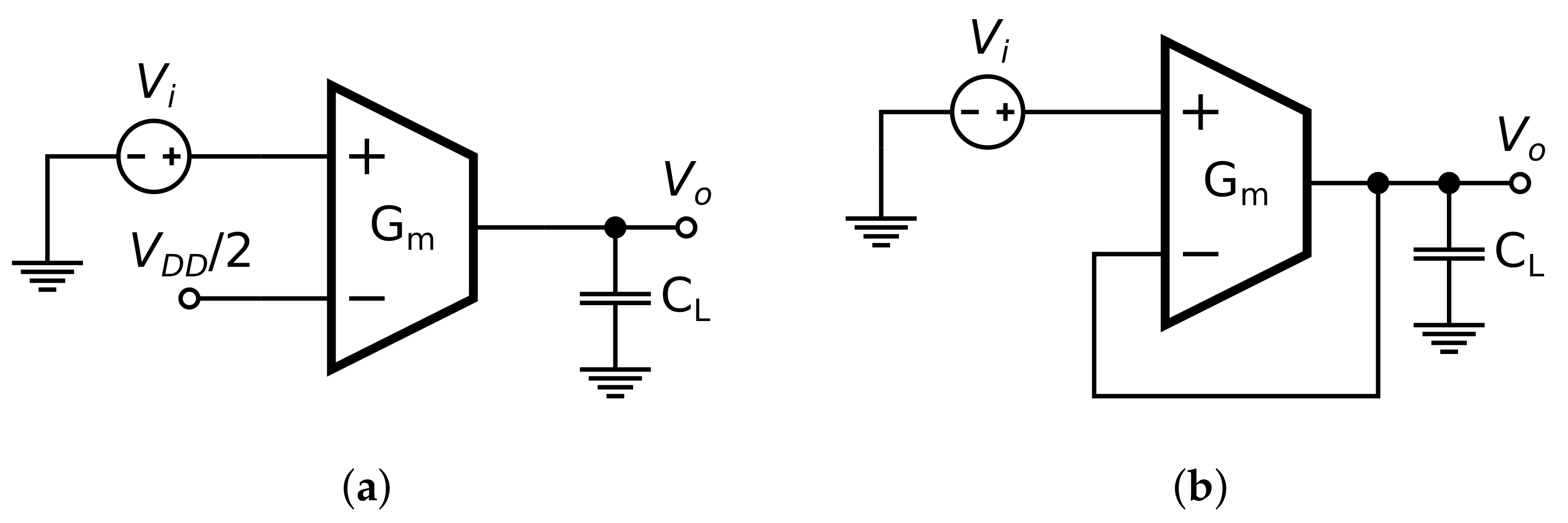
The performance of the proposed OTA, designed in TSMC 180 nm CMOS technology, operating at 27 C, at 0.3 and 0.6 V supply voltages, has been validated by using an open-loop and non-inverting buffer OTA test-bench circuits with a 10 pF capacitive load , as shown in Figure 10a,b.

Figure 10.
OTAs testbench circuits: (a) open-loop (Gm-C integrator); (b) non-inverting buffer.
5.1. Open-Loop Analysis
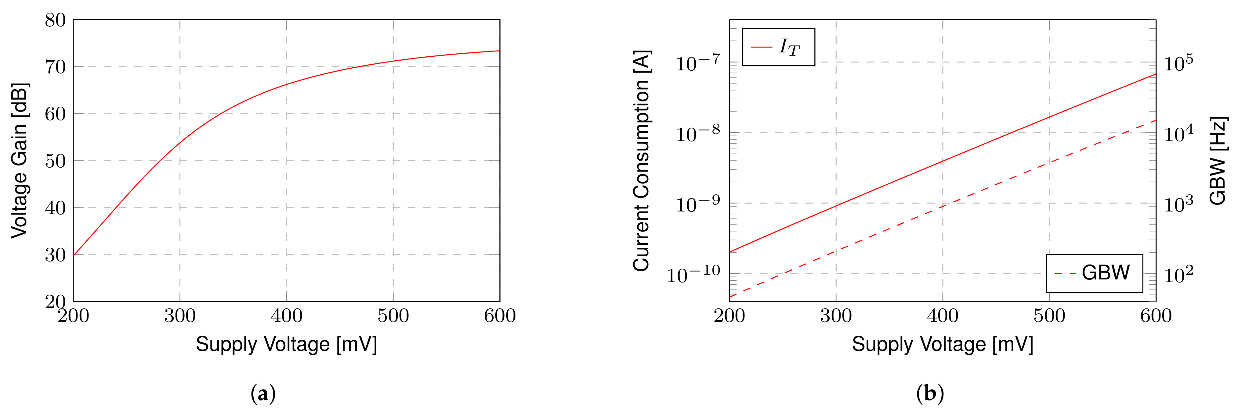
Figure 11 shows how voltage gain and power consumption are affected by the supply voltage variation. In particular, Figure 11a shows that, at the lowest supply voltages, the voltage gain increases exponentially until the supply voltage reaches approximately 400 mV. At higher supply voltages, the improved composite transistor voltage gain technique progressively loses its effectiveness, as expected from the results shown in Figure 3b.

Figure 11.
Voltage supply dependence: (a) voltage gain; (b) total current consumption IT and gain–bandwidth product (GBW).
Figure 11b shows how the current consumption and the gain–bandwidth product (GBW) are affected by the supply voltage variation. The OTA power consumption increases exponentially with the supply voltage, and its gain–bandwidth product GBW increases proportionately, as the inverter transconductance for the weak inversion operation is also proportional to its current consumption [21,22].
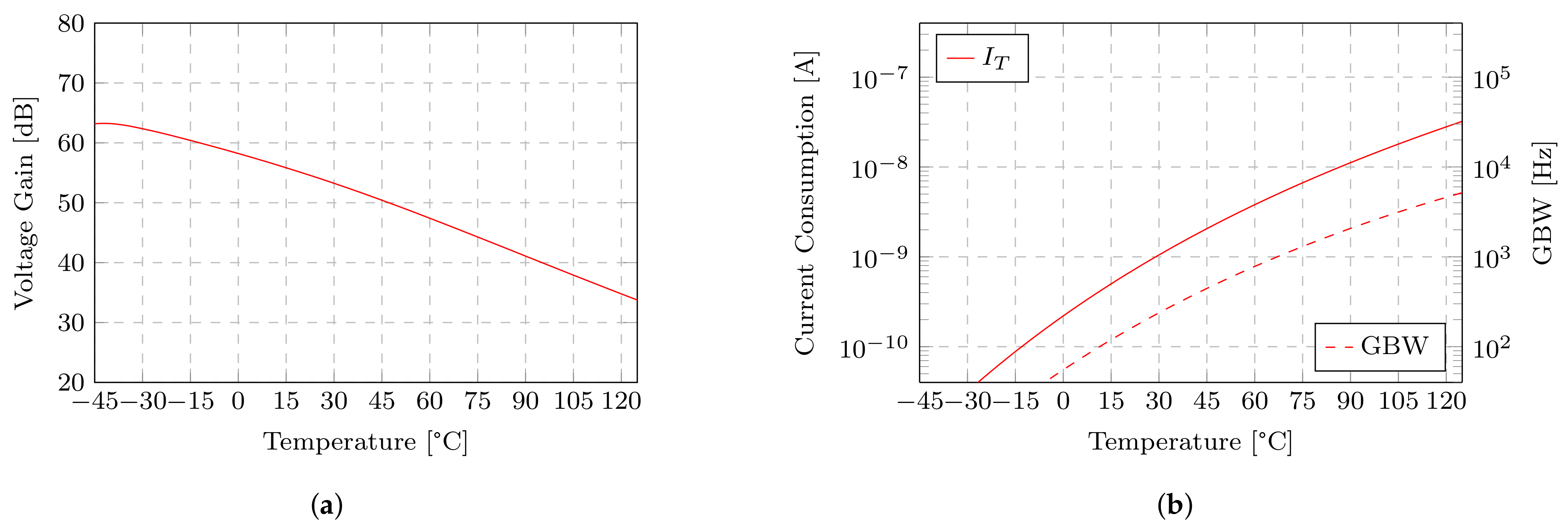
Figure 12a,b shows how voltage gain and power consumption are affected by temperature variation for a 0.3 V voltage supply. As temperature increases, the voltage gain decreases, as a direct result from and reduction, as can be directly inferred from (6) and (4). Furthermore, as the temperature increases, the total current increases as a consequence of the threshold voltage reduction, and GBW increases accordingly.
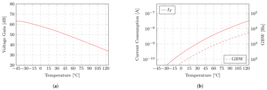
Figure 12.
Temperature dependence: (a) voltage gain, (b) total current consumption IT and gain–bandwidth product (GBW).
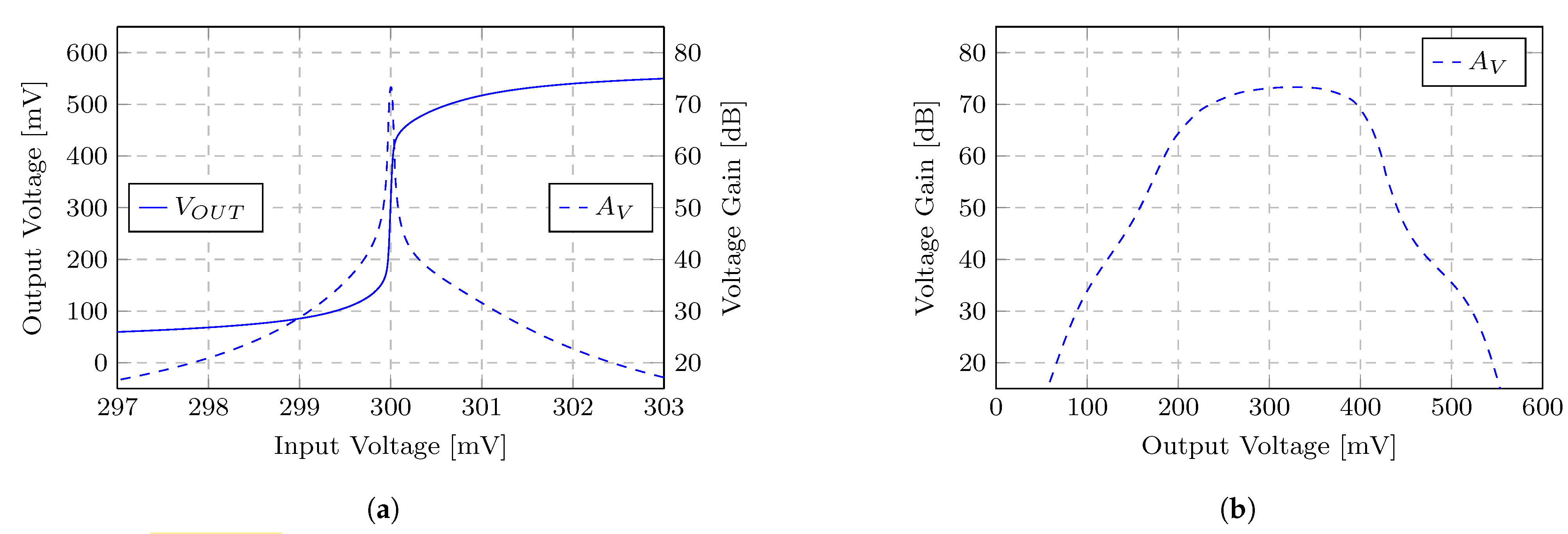
Figure 13a,b, respectively, show the proposed OTA input–output characteristic and the gain of the OTAs versus output voltage for a voltage supply V, while Figure 14a,b show the results for V. It can be noticed that in Figure 13b and Figure 14b, the output voltage affects the OTA voltage gain as a consequence of the reverse transistor current and channel length modulation [22]; therefore, the output conductance varies accordingly. For these reasons, considering a gain dB, output voltage swings between 100 and 500 mV can be obtained for the proposed OTA while supplied with V. The output range limitation is imposed by either PMOS or NMOS transistors entering the linear region outside these limits. For V, the reverse transistor current dominates the output conductance behavior and voltage gain reaches its peak while the input is about half . This is a very important aspect, as small-signal voltage gain can be misleading because it shows only the maximum voltage gain, and voltage gain should be large for a large output voltage range to ensure good signal linearity for any OTA applications with feedback circuits.

Figure 13.
DC open-loop results for VDD = 0.3 V: (a) input–output characteristic, and (b) voltage gain
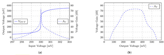
Figure 14.
DC open-loop results for VDD = 0.6 V: (a) input–output characteristic, and (b) voltage gain.
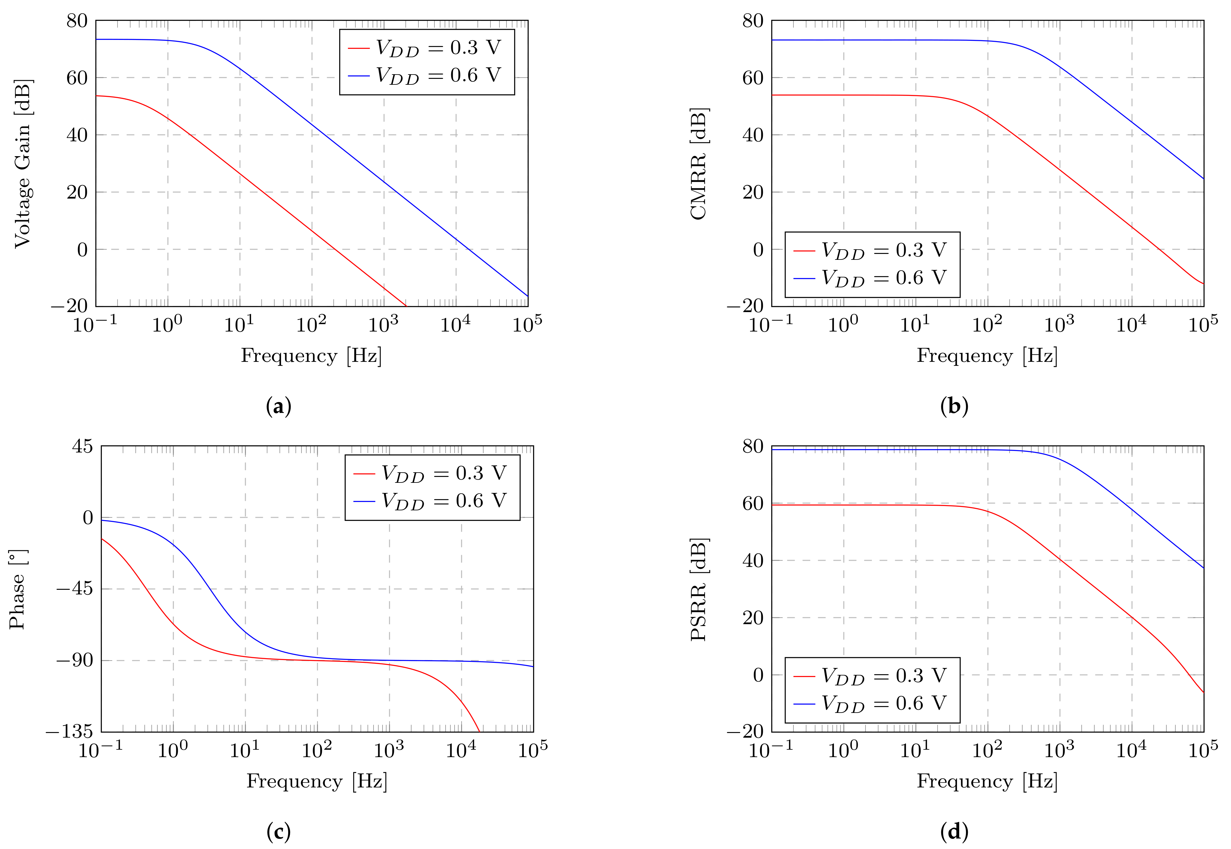
Figure 15a–d shows the AC differential voltage gain, common-mode rejection ratio (CMRR), output phase and power supply rejection ratio (PSRR) curves, respectively. As expected, voltage gain and GBW exhibit large variations according to voltage supplies. The proposed OTA has voltage gains of 54 and 72 dB and a GBW of 102.1 and 14.95 kHz for and , respectively. As the proposed OTAs is a single-stage amplifier, its phase margin is 90. The CMRR are 54 and 72 dB, and PSRR are 59 and 79 dB, respectively.
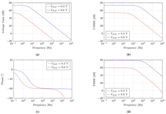
Figure 15.
Open-loop AC simulation results: (a) voltage gain; (b) common-mode rejection ratio (CMRR); (c) phase; (d) power supply rejection ratio (PSRR)
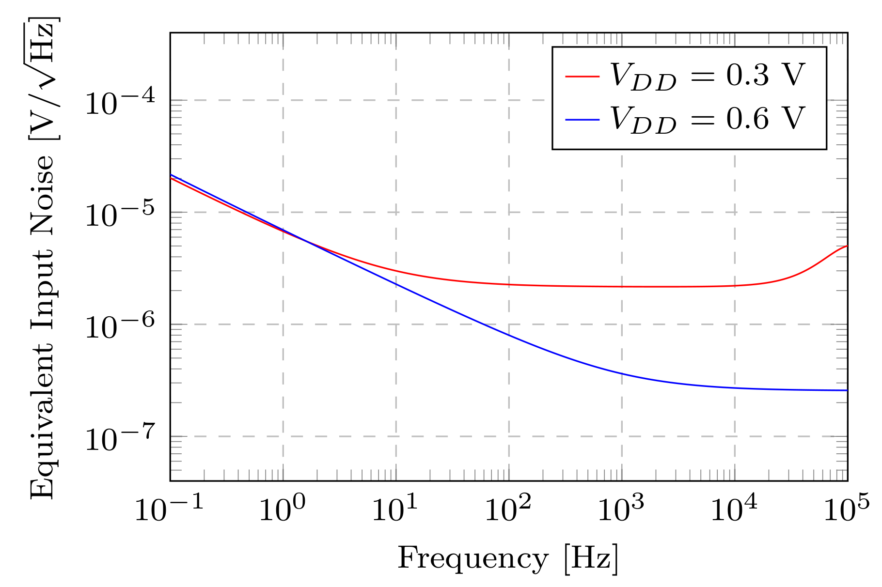
Figure 16 shows the proposed OTA equivalent input referred noise. For , it has equivalent input noises of 2.16 V/, at 1 kHz, and 34.7 V integrated input noise from 1 to 210 Hz. For , it has equivalent input noises of 362 nV/, at 1 kHz, and 39.5 V integrated input noise from 1 to 15 kHz.
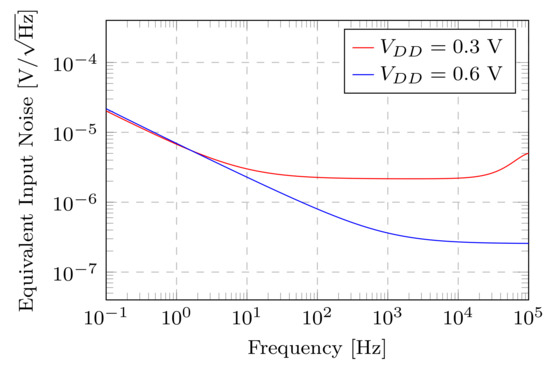
Figure 16.
Input referred noise.
5.2. Unity-Gain Buffer Analysis
As with the output voltage swing limitations observed in open-loop DC simulations (as in Figure 10a), the non-inverting buffer simulations (as in Figure 10) also reveal the limits of input voltage swing, which are shown in Figure 17 and Figure 18.
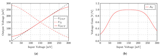
Figure 17.
Non-inverting buffer DC simulation results for VDD = 0.3 V: (a) input–output characteristic and (b) voltage gain.
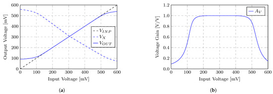
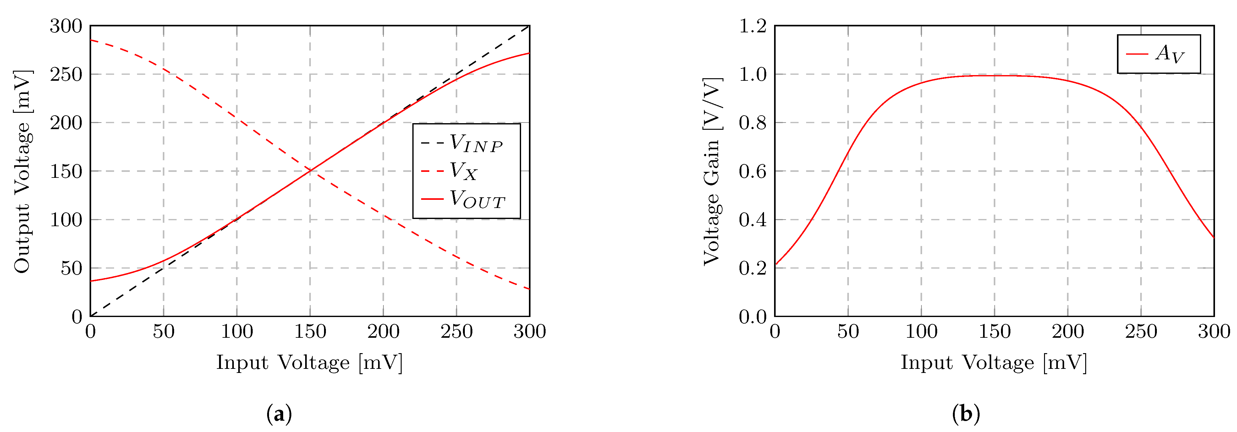
Figure 18.
Non-inverting buffer DC simulation results for VDD = 0.6 V: (a) input–output and (b) voltage gain.
In particular, Figure 18a shows how the output voltage saturation is a consequence of the voltage gain from the input INP to node X (see Figure 7). The X node voltage potential can be expressed as approximately , where is the inverter quiescent voltage [21]. As expected, is approximately the inverted positive input voltage signal . However, is clipped at approximately 100 and 500 mV for the proposed OTA for V, as the inverting voltage buffer does not work properly as the transistors enter the linear operation region.
Figure 17a,b and Figure 18a,b show the main difference between the proposed OTA operation at different voltage supplies for the non-inverting buffer configuration. For V, the OTA has a more linear output due to its higher open-loop voltage gain and larger output voltage excursion, as expected. The OTAs proposed in [19] use a similar topology with half the number of inverters, but the voltage excursion is also limited by the transistor slope factor n, which further limits those OTAs input range compared to the OTAs proposed in this work.
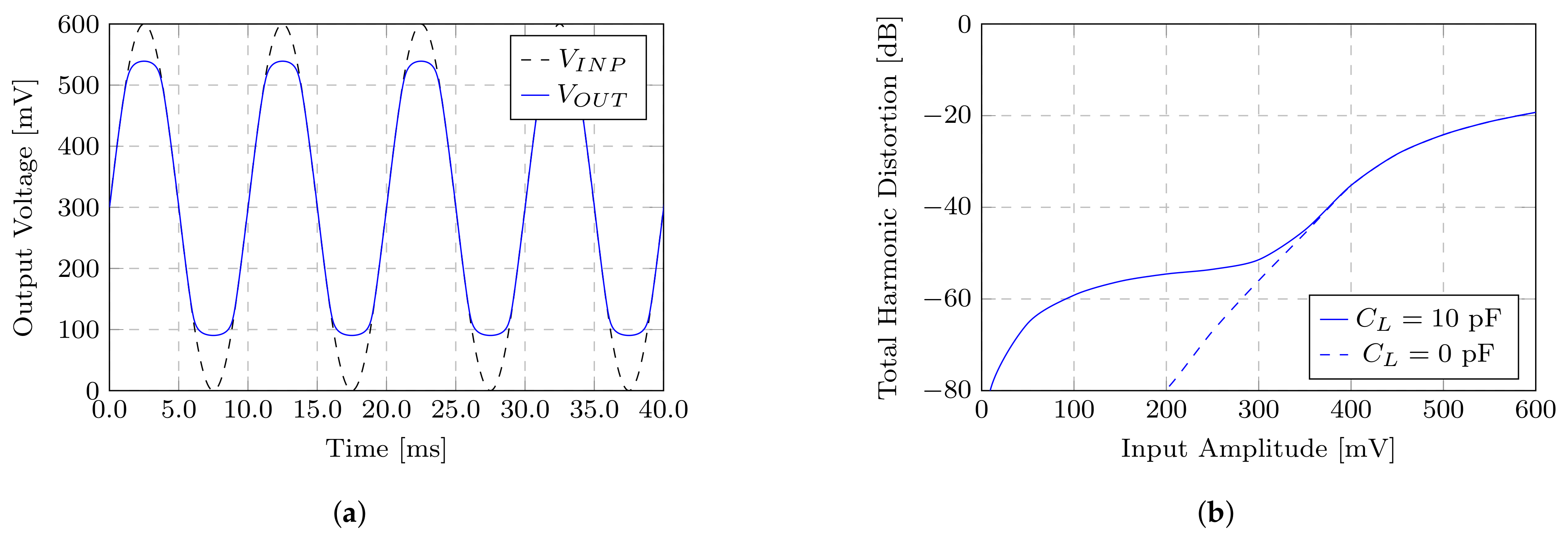
The same limitations, from the point of view of time-domain, are shown in Figure 19a,b and Figure 20a,b for a rail-to-rail input sine-wave for V and V, respectively. The corresponding total harmonic distortion (THD) is displayed in Figure 17b and Figure 18b for a 10 pF capacitive load and no load except from the input impedance resulted from connecting the OTA output to the inverting input. A total harmonic distortion of 1% is achieved for input peak-to-peak amplitudes ranges of 300 and 375 mV for V and V, respectively. For lower input voltage amplitudes and no output load, the proposed OTA shows an even better linearity, achieving 80 dB THD for a 200 mV input amplitude for V. This is a direct consequence of the DC characteristic curves shown in Figure 18a,b, due to its higher open-loop voltage gain and that GBW is many times higher for lower capacitive loads. By analyzing Figure 18b, it is made clear that the main limitations to the output signal linearity are the signal frequency, OTA GBW and the OTA DC characteristic curve.
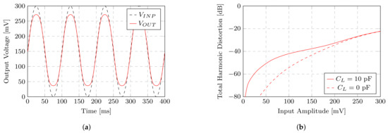
Figure 19.
Non-inverting buffer transient simulation results: (a) sine-wave output response; (b) total harmonic distortion.
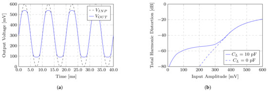
Figure 20.
Non-inverting buffer transient simulation results: (a) sine-wave output response; (b) total harmonic distortion.
5.3. Monte Carlo Simulation Results
Table 1 summarizes the corner simulation results. As expected, the greatest deviations from typical corner results are GBW and power for SS (Slow-Slow) and FF (Fast-Fast) corners. The worst corners for intrinsic input offset are SF (Slow-Fast) and FS (Fast-Slow), as the inverter transistor dimensions were optimized for the typical corner TT. As explained before, the OTA linearity is a function of the internal node voltage , and input signal frequency and GBW. For better performance stability, PVT variability could be reduced by extra biasing circuits [21] or calibration [27].

Table 1.
Corner results.
Table 2 summarizes the mean and the standard variation from 1000 Monte Carlo simulation runs. Process and mismatch variations are analyzed individually and combined. The OTA results show that gain–bandwidth product GBW, total current , and power consumption are greatly affected by the process variability, as suggested by corner results. The power efficiency Figure of Merit, FoM, defined as , shows a negligible variation, since GBW is somehow proportional to , as shown in Figure 11b. It is the same for the open-loop voltage gain. As a main drawback, the mismatch variations strongly affect the offset voltage of both OTAs. The simulations show 8.7 and 8.9 mV input offset voltage for 3 mismatch variation for V and V, respectively.

Table 2.
Monte Carlo results.
5.4. Performance Comparison
Table 3 summarizes the proposed OTA results and compares them to the state-of-art counterparts. The state-of-art OTAs can be categorized by the input terminal of their first stage amplifier block, and can be gate-driven [19,21,24,27,28,29,30,31] and bulk-driven [18,28,32,33,34]. Gate-driven OTAs are usually more power-efficient, as the bulk-drain transconductance is a fraction of the gate-drain transconductance, while bulk-driven OTAs have an extended voltage input range, which leads to less signal distortion for larger voltage signal amplitudes.

Table 3.
Perfomance comparison.
Additionally, the OTAs reported in Table 3 are classified as single-ended and fully differential. The fully differential circuits use more area and power, but their signals are more insensitive to power and common-mode fluctuations, and they have increased voltage range and output less distortion.
The proposed OTAs main feature is its voltage gain per number of stages, while still maintaining a relatively small area, a high power-efficiency figure of merit, and a high linearity for an extremely low voltage supply. A higher voltage gain could be achieved by using more amplifier stages; however, it would come at the cost of more area and the need for a stability compensation circuit.
The best power-efficient design for a 0.3 V supply voltage was proposed in [27], with a 1020 FoM. The proposed design has a 229 FoM, which is 4.45× smaller. However, it has a 1% THD for a 120 mV peak-to-peak amplitude signal, while the former has a 3% THD for a 100 mV peak-to-peak amplitude signal. As compared to the other state-of-art designs with supply voltage under 0.3 V, despite having a single gain stage, it still has the second best voltage gain. The best voltage gain under 0.3 V supply voltage [32] is 60 dB; however, as it is a multiple-stage OTA design, it has an area 25× larger, whereas the proposed OTA would have a 40 dB voltage gain for the same supply voltage at 0.25 V. The best voltage gain among all OTAs [18] has an 81 dB voltage gain at a 0.4 V supply voltage. The proposed OTA can achieve a 66 dB voltage gain with a single gain stage alone at 0.4 V supply voltage and has a total area about 5× smaller.
The best comparison can be made with the inverter-based OTA proposed in [21], as it was designed for the same process using the same transistor dimensions and voltage supply. For V, it has 1.4× more area and about half of its power-efficiency FoM; however, it has a 3.4× larger input voltage excursion for the same THD. It also has a slightly larger voltage gain.
6. Conclusions
This paper shows how to maximize the gain of an inverter-based OTA topology with independently forward-body-biased composite transistors without reducing its input voltage swing. Compared with other state-of-art OTAs in similar operation conditions, the proposed OTAs have the largest voltage gain by the number of amplifier gain stages (54 dB at 0.3 V and 73 dB at 0.6 V ), while still keeping a relatively small die area (1026 ). Notice that the same technique could also be exploited in fully differential inverter-based OTA topologies.
Author Contributions
Conceptualization, L.H.R.; methodology, L.H.R. and O.A.; validation, L.H.R.; formal analysis, L.H.R. and O.A.; investigation, L.H.R.; resources, C.R.R.; data curation, L.H.R.; writing—original draft preparation, L.H.R.; writing—review and editing, O.A. and C.R.R.; visualization, L.H.R.; supervision, O.A. and C.R.R.; project administration, C.R.R.; funding acquisition, C.R.R. All authors have read and agreed to the published version of the manuscript.
Funding
This research was funded by Coordenação de Aperfeiçoamento de Pessoal de Nível Superior (CAPES).
Data Availability Statement
Data is contained within the article.
Acknowledgments
The authors would like to thank Europractice and TSMC for PDK access.
Conflicts of Interest
The authors declare no conflict of interest.
Abbreviations
The following abbreviations are used in this manuscript:
| CMOS | Complementary Metal-Oxide Semiconductor |
| CMRR | Common-Mode Rejection Ratio |
| FoM | Figure of Merit |
| GBW | Gain–Bandwidth Product |
| OTA | Operational Transconductance Amplifier |
| PSRR | Power Supply Rejection Ratio |
| THD | Total Harmonic Distortion |
| UICM | Unified Current Control Model |
| ULP | Ultra-Low-Power |
| ULV | Ultra-Low-Voltage |
References
- Crovetti, P.S.; Musolino, F.; Aiello, O.; Toledo, P.; Rubino, R. Breaking the boundaries between analogue and digital. Electron. Lett. 2019, 55, 672–673. [Google Scholar] [CrossRef]
- Aiello, O.; Crovetti, P.; Alioto, M. A Sub-Leakage pW-Power Hz-Range Relaxation Oscillator Operating with 0.3 V–1.8 V Unregulated Supply. In Proceedings of the IEEE Symp. on VLSI Circuits (VLSI 2018), Honolulu, HI, USA, 18–22 June 2018; pp. 119–120. [Google Scholar]
- Aiello, O.; Crovetti, P.; Lin, L.; Alioto, M. A pW-Power Hz-Range Oscillator Operating With a 0.3–1.8-V Unregulated Supply. IEEE J. Solid-State Circuits 2019, 54, 1487–1496. [Google Scholar] [CrossRef]
- Aiello, O.; Crovetti, P.; Alioto, M. Wake-Up Oscillators with pW Power Consumption in Dynamic Leakage Suppression Logic. In Proceedings of the IEEE Int. Symposium on Circuits and Systems (ISCAS 2019), Sapporo, Japan, 26–29 May 2019; pp. 1–5. [Google Scholar]
- Aiello, O.; Crovetti, P.; Alioto, M. Ultra-Low Power and Minimal Design Effort Interfaces for the Internet of Things: Invited paper. In Proceedings of the IEEE 2019 Int. Circuit and System Symp. (ICSyS), Kuala Lumpur, Malaysia, 18–19 September 2019; pp. 1–5. [Google Scholar]
- de Aguirre, P.C.C.; Bonizzoni, E.; Maloberti, F.; Susin, A.A. A 170.7-dB FoM-DR 0.45/0.6-V Inverter-Based Continuous-Time Sigma–Delta Modulator. IEEE Trans. Circuits Syst. II 2020, 67, 8,1384–1388. [Google Scholar] [CrossRef]
- Aiello, O.; Crovetti, P.; Alioto, M. Fully Synthesizable Low-Area Analogue-to-Digital Converters with Minimal Design Effort Based on the Dyadic Digital Pulse Modulation. IEEE Access 2020, 8, 70890–70899. [Google Scholar] [CrossRef]
- Aiello, O.; Crovetti, P.; Alioto, M. Capacitance-to-Digital Converter for Operation under Uncertain Harvested Voltage down to 0.3V with No Trimming, Reference and Voltage Regulation. In Proceedings of the IEEE 2021 International Solid-State Circuits Conference (ISSCC 2021), San Francisco, CA, USA, 13–22 February 2021; pp. 74–76. [Google Scholar]
- Aiello, O.; Crovetti, P.; Toledo, P.; Alioto, M. Rail-to-rail dynamic voltage comparator scalable down to pw-range power and 0.15-v supply. IEEE Trans. Circuits Syst. II 2021. [Google Scholar] [CrossRef]
- Richelli, A.; Colalongo, L.; Kovacs-Vajna, Z.; Calvetti, G.; Ferrari, D.; Finanzini, M.; Pinetti, S.; Prevosti, E.; Savoldelli, J.; Scarlassara, S. A Survey of Low Voltage and Low Power Amplifier Topologies. J. Low Power Electron. Appl. 2018, 8, 22. [Google Scholar] [CrossRef]
- Nauta, B. A CMOS transconductance-C filter technique for very high frequencies. IEEE J. Solid-State Circuits 1992, 27, 142–153. [Google Scholar] [CrossRef]
- Barthelemy, H.; Meillere, S.; Gaubert, J.; Dehaese, N.; Bourdel, S. OTA based on CMOS inverters and application in the design of tunable bandpass filter. Analog Integr. Circuits Signal Process. 2008, 57, 169–178. [Google Scholar] [CrossRef]
- Vlassis, S. 0.5 V CMOS inverter-based tunable transconductor. Analog Integr. Circuits Signal Process. 2012, 72, 289–292. [Google Scholar] [CrossRef]
- Vieru, R.G.; Ghinea, R. An ultra low voltage sigma delta modulator with inverter based scalable amplifier. In Proceedings of the 2012 10th International Symposium on Electronics and Telecommunications, Timisoara, Romania, 15–16 November 2012; pp. 3–6. [Google Scholar]
- Khateb, F.; Kulej, T.; Vlassis, S. Extremely low-voltage bulk-driven tunable transconductor. Circuits Syst. Signal Process. 2017, 36, 511–524. [Google Scholar] [CrossRef]
- Centurelli, F.; Della Sala, R.; Scotti, G.; Trifiletti, A. A 0.3 V, Rail-to-Rail, Ultralow-Power, Non-Tailed, Body-Driven, Sub-Threshold Amplifier. Appl. Sci. 2021, 11, 2528. [Google Scholar] [CrossRef]
- Kulej, T.; Khateb, F. A 0.3-V 98-dB Rail-to-Rail OTA in 0.18 μm CMOS. IEEE Access 2020, 8, 27459–27467. [Google Scholar]
- Baghtash, H.F. A 0.4 V, body-driven, fully differential, tail-less OTA based on current push-pull. Microelectron. J. 2020, 99, 104768. [Google Scholar]
- Rodovalho, L.H.; Aiello, O.; Rodrigues, C.R. Ultra-Low-Voltage Inverter-Based Operational Transconductance Amplifiers with Voltage Gain Enhancement by Improved Composite Transistors. Electronics 2020, 9, 1410. [Google Scholar] [CrossRef]
- Niranjan, V.; Kumar, A.; Jain, S.B. Composite transistor cell using dynamic body bias for high gain and low-voltage applications. J. Circuits Syst. Comput. 2014, 23, 1450108. [Google Scholar] [CrossRef]
- Rodovalho, L.H. Push–pull based operational transconductor amplifier topologies for ultra low voltage supplies. Analog. Integr. Circuits Signal Process. 2020, 1–14. [Google Scholar] [CrossRef]
- Schneider, M.C.; Galup-Montoro, C. CMOS Analog Design Using All-Region MOSFET Modeling; Cambridge University Press: Cambridge, UK, 2010. [Google Scholar]
- Galup-Montoro, C.; Schneider, M.C.; Loss, I.J. Series-parallel association of FET’s for high gain and high frequency applications. IEEE J. Solid-State Circuits 1994, 29, 1094–1101. [Google Scholar] [CrossRef]
- Braga, R.A.; Ferreira, L.H.; Coletta, G.D.; Dutra, O.O. A 0.25-V calibration-less inverter-based ota for low-frequency gm-c applications. Microelectron. J. 2019, 83, 62–72. [Google Scholar] [CrossRef]
- Lindert, N.; Sugii, T.; Tang, S.; Hu, C. Dynamic threshold pass-transistor logic for improved delay at lower power supply voltages. IEEE J. Solid-State Circuits 1999, 34, 85–89. [Google Scholar] [CrossRef]
- Clerc, S. The Fourth Terminal: Benefits of Body-Biasing Techniques for FDSOI Circuits and Systems; Springer Nature: Berlin/Heidelberg, Germany, 2020. [Google Scholar]
- Toledo, P.; Aiello, O.; Crovetti, P. A 300mV-Supply Standard-Cell-Based OTA with Digital PWM Offset Calibration. In Proceedings of the IEEE Nordic Conference of Circuits and Systems, Helsinki, Finland, 29–30 October 2019. [Google Scholar]
- Chatterjee, S.; Tsividis, Y.; Kinget, P. 0.5-V analog circuit techniques and their application in OTA and filter design. IEEE J. Solid-State Circuits 2005, 40, 2373–2387. [Google Scholar] [CrossRef]
- Toledo, P.; Crovetti, P.; Aiello, O.; Alioto, M. Fully-Digital Rail-to-Rail OTA with Sub-1,000 μm2 Area, 250-mV Minimum Supply and nW Power at 150-pF Load in 180 nm. IEEE Solid-State Circuits Lett. 2020, 3, 474–477. [Google Scholar] [CrossRef]
- Lv, L.; Zhou, X.; Qiao, Z.; Li, Q. Inverter-Based Subthreshold Amplifier Techniques and Their Application in 0.3-V Delta Sigma Modulators. IEEE J. Solid-State Circuits 2019, 54, 1436–1445. [Google Scholar] [CrossRef]
- Manfredini, G.; Catania, A.; Benvenuti, L.; Cicalini, M.; Piotto, M.; Bruschi, P. Ultra-Low-Voltage Inverter-Based Amplifier with Novel Common-Mode Stabilization Loop. Electronics 2020, 9, 1019. [Google Scholar] [CrossRef]
- Ferreira, L.H.; Sonkusale, S.R. A 60-dB gain OTA operating at 0.25-V power supply in 130-nm digital CMOS process. IEEE Trans. Circuits Syst. I Regul. Pap. 2014, 61, 1609–1617. [Google Scholar] [CrossRef]
- Abdelfattah, O.; Roberts, G.W.; Shih, I.; Shih, Y.C. An ultra-low-voltage CMOS process-insensitive self-biased OTA with rail-to-rail input range. IEEE Trans. Circuits Syst. I Regul. Pap. 2015, 62, 2380–2390. [Google Scholar] [CrossRef]
- Veldandi, H.; Shaik, R.A. A 0.3-v pseudo-differential bulk-input ota for low-frequency applications. Circuits Syst. Signal Process. 2018, 37, 5199–5221. [Google Scholar] [CrossRef]
Publisher’s Note: MDPI stays neutral with regard to jurisdictional claims in published maps and institutional affiliations. |
© 2021 by the authors. Licensee MDPI, Basel, Switzerland. This article is an open access article distributed under the terms and conditions of the Creative Commons Attribution (CC BY) license (https://creativecommons.org/licenses/by/4.0/).


