Article

Analysis and Design of a Fully-Integrated High-Power Differential CMOS T/R Switch and Power Amplifier Using Multi-Section Impedance Transformation Technique

1
Broadcom, San Jose, CA 95131, USA
2
Qualcomm, San Diego, CA 92121, USA
3
Department of Electrical Engineering, Pusan National University, Busan 46241, Korea
4
Department of Electrical and Computer Engineering, California State Polytechnic University, Pomona, CA 91768, USA
5
Qualcomm, San Jose, CA 95110, USA
*
Author to whom correspondence should be addressed.
Electronics 2021, 10(9), 1028; https://doi.org/10.3390/electronics10091028
Submission received: 24 March 2021 / Revised: 23 April 2021 / Accepted: 24 April 2021 / Published: 26 April 2021
(This article belongs to the Section Circuit and Signal Processing)

Abstract

:
In this paper, a new topology for a high-power single-pole-double-throw (SPDT) antenna switch is presented, and its loss mechanisms are fully analyzed. The differential architecture is employed in the proposed switch implementation to prevent unwanted channel formations of OFF-state Rx switch transistors by relieving the voltage swing over the Rx switch devices. In addition to that, the load impedance seen by the Tx switch is stepped down to reduce the voltage swing even more, allowing the antenna switch to handle a high-power signal without distortions. To drop the switch operating impedance, two matching networks are required at the input and the output of the Tx switch, respectively, and they are carefully implemented considering the integration issue of the front-end circuitries. From the loss analysis of the whole signal path, an optimum switch operating impedance is decided in view of a trade-off between power handling capability and insertion loss of the antenna switch. The insertion loss of the proposed design is compared to the conventional design with electromagnetic (EM) simulated transformer and inductors. The proposed antenna switch is implemented in a standard 0.18 µm CMOS process, and all switch devices adopt the deep n-well structure. The measured performance of the proposed transmitter front-end chain shows a 1 dB compression point (P1dB) of 32.1 dBm with 38.3% power-added efficiency (PAE) at 1.9 GHz.

1. Introduction

The full integration of radio frequency (RF) functional building blocks is a design trend in wireless communication applications [1]. The integration trend is mainly driven by the explosive demand for low-cost transceiver solutions for various wireless applications. Therefore, CMOS technology is in the spotlight as the potential candidate to achieve the fully integrated RF transceiver, thanks to its low cost and high feasibility of integration. However, it is very challenging to realize the fully integrated CMOS radio because of some flaws embedded in the process itself. Particularly, the CMOS implementation is not suitable for high-power-handling components such as power amplifiers (PAs) and antenna switches due to low breakdown voltage and substrate parasitic components of active devices.
There have been numerous efforts to overcome these drawbacks in the RF antenna switch design. Multiple transistors were stacked to secure the device reliability [2]. The LC tuned substrate technique was applied to prevent junction diodes from forward biasing [3]. In addition, the body floating technique was devised with triple-well devices [4]. As another attempt to enhance the power performance of switches, the impedance transformation technique and the differential architecture were introduced [5,6]. Most recently, the body isolation technique was used with an LC resonate Rx switch, resulting in 30 dBm of P1dB [7]. In addition, more than a Watt-level of P1dB was achieved by using switch devices with a sub-design-rule (SDR) length and feed-forward capacitors [8]. However, the P1dB of the antenna switch still needs to be improved to a higher level to make the switch robust to the antenna mismatch. In addition, even higher than 2-W levels of output power should be handled by the antenna switch in some mobile applications. For example, the antenna switch using silicon-on-insulator (SOI) or gallium-arsenide (GaAs) material shows more than 37 dBm of P1dB [9,10,11,12].
In this paper, we propose a new topology for a high-power antenna switch that handles more than 2-W level of power, employing a multi-section impedance transformation technique with a differential architecture, as shown in Figure 1b. Although additional matching networks are required to control the switch operating impedance as presented in [5], the number of additional matching networks is minimized in a proposed design by utilizing the PA output matching as a part of the multi-section impedance matching. The multi-section impedance matching also might be a better solution in perspective of total efficiency in some cases [13]. Generally, the output impedance of PAs for Watt-level applications is low to drive more current [14]. Consequently, a highly efficient output matching for PAs is hard to achieve due to the large impedance transformation ratio. In the proposed structure, the burden of impedance transformation is distributed to multi-section matching networks (Figure 1b), instead of transforming at a time with a single matching network (Figure 1a). In short, the proper switch load impedance for high-power switch operation (between the output impedance of the PA and the antenna impedance) can be obtained, minimizing the number of additional matching networks and loss of whole signal path, in a proposed design. For the matching networks, the output transformer of the PA and the LC balun are used, respectively. In this configuration, the total loss depends on factors such as the impedance transformation ratio of matching networks and a switch insertion loss corresponding to a load impedance seen by the switch. In other words, the loss is eventually decided by the switch operating impedance. To select an optimum switch operating impedance, the total loss and power performance of the proposed configuration are analyzed with various switch operating impedances and compared to a conventional switch structure. Although the basic concept of the proposed technique was introduced in [15,16], a more analogous approach is described in this work to expand its applicability. Only T/Rx switches were implemented, and a PA was not included in the works of [15,16]. In addition, a multi-section impedance transformation network was adopted with off-chip baluns [16] or load-pull equipment [15]. In this work, a fully integrated differential T/Rx switches and a power amplifier using a multi-section impedance transformation network was implemented, and the measurement results demonstrate the operation of the proposed technique.
The paper is organized as follows. In Section 2, the differential switch using the multi-section impedance transformation technique is described and explained briefly. The loss analysis for each block is presented in Section 3, and the proposed switch design and its implementation follow in Section 4. The measurement results for the stand-alone differential switch are shown in Section 5, and conclusions are given in Section 6.

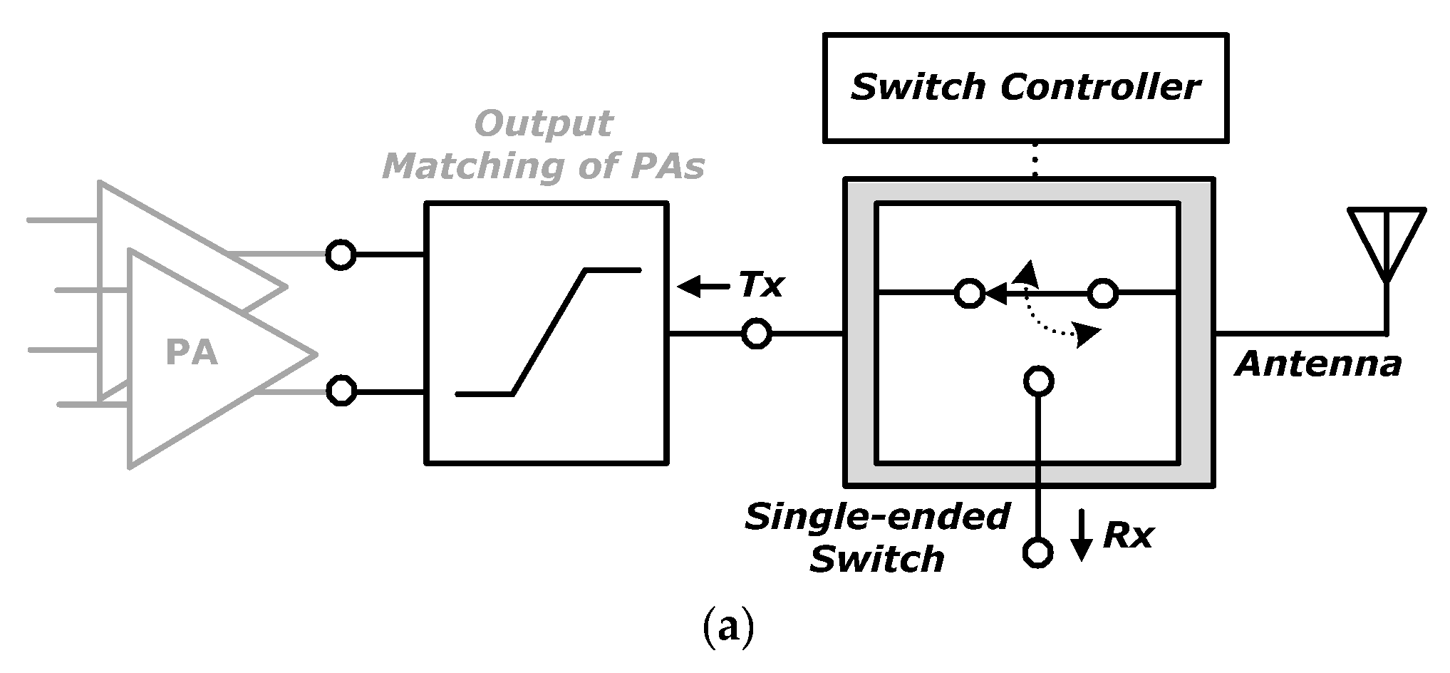
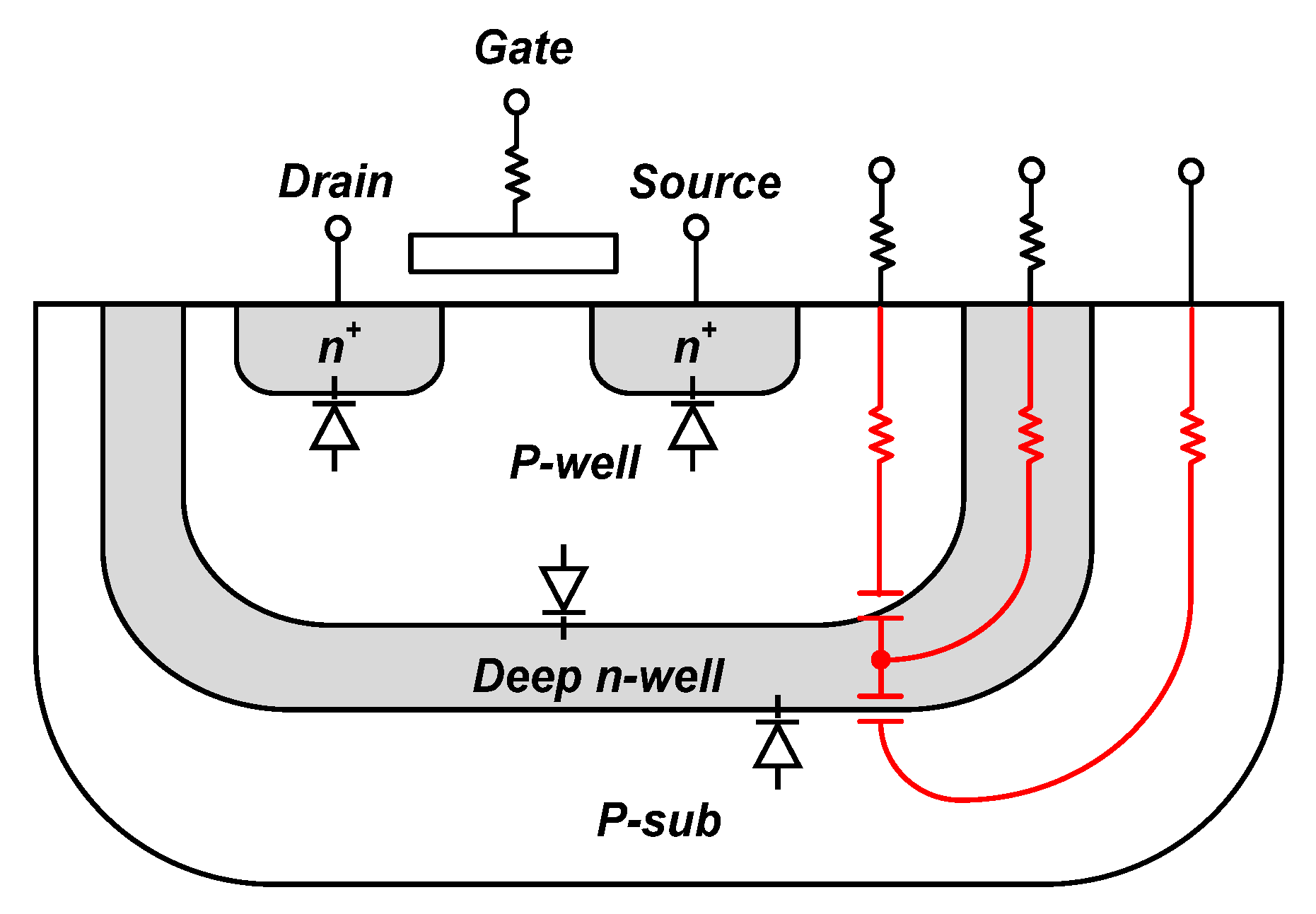
2. Proposed High-Power CMOS T/R Switch Structure

The power-handling capability of the antenna switch is mainly limited by the large voltage swing of the high-power signal over the switch devices in Tx mode. While signal is passing through an ON-state Tx switch, negative voltage peaks of the RF signal are limited by the turn-on voltage of junction diodes. On the other hand, when a large voltage stress is loaded over the OFF-state Rx switch, the voltage swing is limited not only by the turn-on voltage of junction diodes but also by the threshold voltage and breakdown voltage of OFF-state devices. Therefore, the power performance of the antenna switch can be improved effectively by reducing the voltage swing over switch devices.
As one of the methods to relieve the voltage swing, the differential topology is proposed in this design. The differential switch consists of two identical single-ended switches, providing two signal paths. As a result, the voltage swing on each single-ended switch can be reduced in half, while the antenna switch transmits the same power at the antenna port. Secondly, the impedance transformation technique is applied to reduce the voltage swing even more. The large voltage swing, which is demanded to transmit a certain level of power, is relaxed by stepping down the load impedance seen by the antenna switch [5]. As shown in Figure 2, voltage swings over each single-ended switch path are reduced by employing the differential structure, and they are decreased more as the switch operating impedance reduces. In spite of these voltage reduction techniques, the voltage stress over OFF-state switches are still large when high power signal transmits, so multiple switch devices are stacked for OFF-state switches to distribute the stress to multiple devices [2]. The number of stacked transistors is strictly limited by the insertion loss in Rx mode, and the number can be minimized in the proposed structure, reducing the size of voltage swing as much as possible. In summary, the power-handling capability of the antenna switch is enhanced by utilizing the impedance transformation technique with the differential architecture, as shown in Figure 3.
In employing the impedance transformation technique, the matching networks are implemented aiming to the fully integrated front-end with the PA. For the matching network at the transmitter side, a transformer is utilized. While the transformer functions as a matching network, it also combines the output powers transmitted from multiple PAs compactly compared to the LC counterpart. Since the power combining is essential to transmit higher power than Watt level, the transformer can be a good candidate for the output matching network of high-power transmitters. For another matching network between the switch and the antenna, the LC balun is implemented. It converts a differential port to a single-ended port to match the unbalanced antenna as well as the transformer impedance. The LC balun is preferred for this matching, since it is easy to achieve the accurate switch operating impedance with the LC balun by manipulating it. Even though all of these functions can be done by one matching network [14], multi-section matching is chosen to lower the switch operating impedance, in other words, to apply the impedance transformation technique. In spite of the additional matching network in the proposed structure, the loss of the multi-section matching network can be lower than that of the single section matching network, according to its impedance transformation ratio and transformation efficiency [17]. The following sections analyzed and compared the loss of the proposed design to the loss of the single matching case.

3. Loss Analysis

The antenna switch is located at the last stage of the transmitter chain and the first stage of the receiver chain at the same time. Therefore, the insertion loss of the antenna switch should be minimized to preserve the efficiency of the transmitter and the noise figure of the receiver. In a proposed structure, the impedance transformation technique is applied to improve the power performance of the antenna switch by lowering the switch operating impedance, and there is a possibility to degrade the insertion loss. Additional matching networks are required to use this technique, and even the insertion loss of the switch itself is exacerbated with the reduced switch operating impedance [5]. Hence, the loss should be optimized by selecting a proper switch operating impedance, controlling the impedance transformation ratio of the matching networks, and minimizing the switch insertion loss.

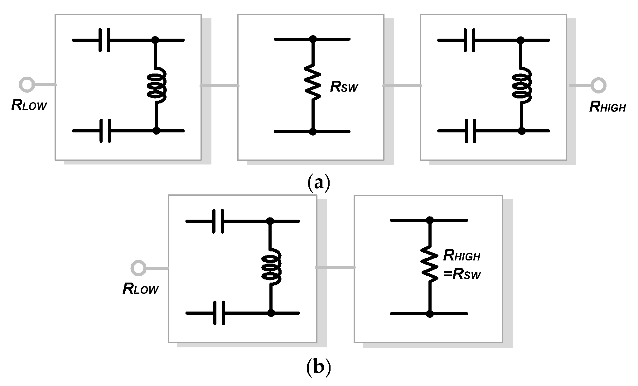
3.1. Multi-Section Impedance Transformation

η = Q 2 + 1 Q 2 + r + r 2 + 4 Q 2 ( r 1 ) 2  
The most straightforward impedance matching method is the LC-type matching. In Figure 4a, the LC matching with single input and single output is presented. As derived in [13], the efficiency of the matching network is defined by Equation (1) where Q is the quality factor (Q-factor) of the inductor used in the matching network and r is the impedance transformation ratio, which is Rload/Rin. The Q-factor of the capacitor is generally much higher than that of the inductor, so the loss due to the capacitor is neglected here. The equation is also valid for the LC matching with differential input and output (Figure 4b). As shown in the equation, the loss of the matching mainly depends on two factors, the Q-factor of the inductor and the impedance transformation ratio.
In the proposed structure, the low output impedance of the PA is transformed to switch the operating impedance by the first matching network, and the impedance is stepped up once again by the second matching network to 50 Ω. To compare the loss of the multi-section matching (Figure 5a) to that of the single-section matching (Figure 5b), the LC matching is utilized in the analysis here. RLOW is assumed as 5 Ω, which is the output impedance of the Watt-level power amplifier and RHIGH is 50 Ω, which is the antenna impedance. As mentioned earlier, the switch operating impedance, RSW, is supposed to be lower than 50 Ω to ensure the high-power performance of the antenna switch but not excessively low to avoid loss degradation. On the other hand, the practical range of the on-chip inductor Q-factor is approximately 5 to 20 at 1.9 GHz, while it is implemented in a standard CMOS process. To achieve the higher inductor Q-factor, an integrated passive device (IPD) or surface mount device (SMD) is required. Based on these practical considerations for the proposed structure, the matching efficiencies according to RSW and inductor Q-factors are plotted in Figure 6. As shown in the graph, the loss of multi-section matching is maintained over a reasonable range of RSW, a distributing large impedance transformation ratio from 5 to 50 Ω.

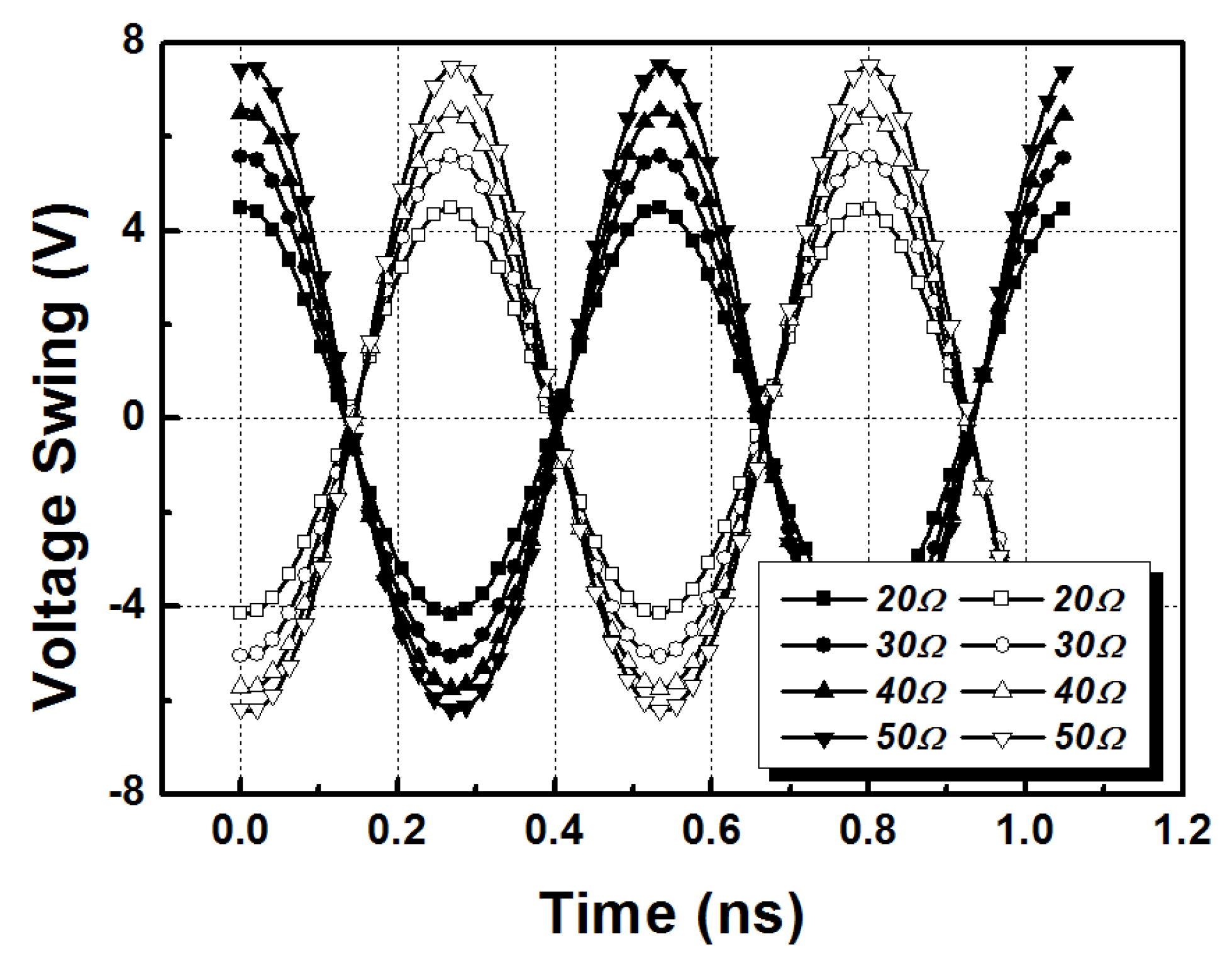
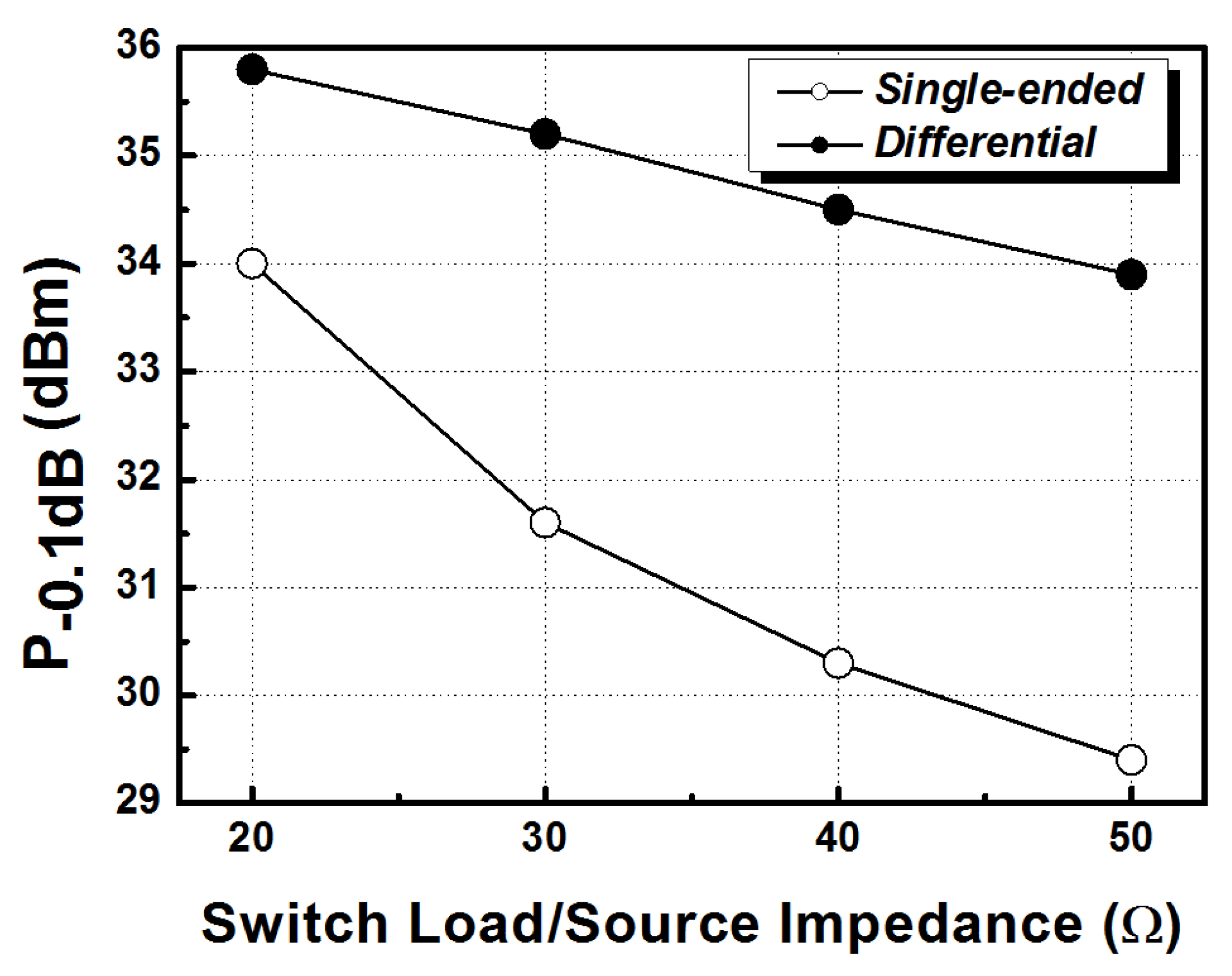
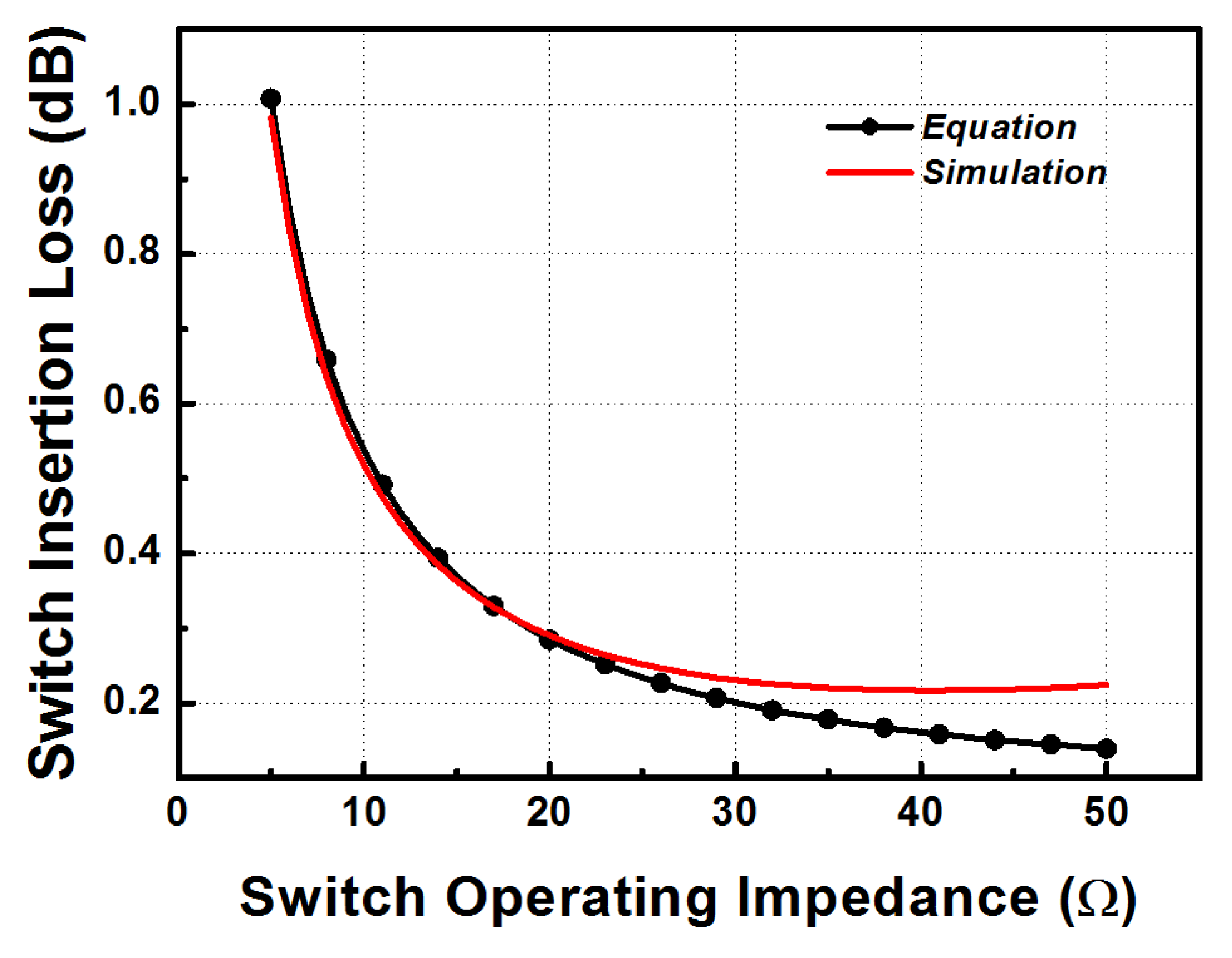
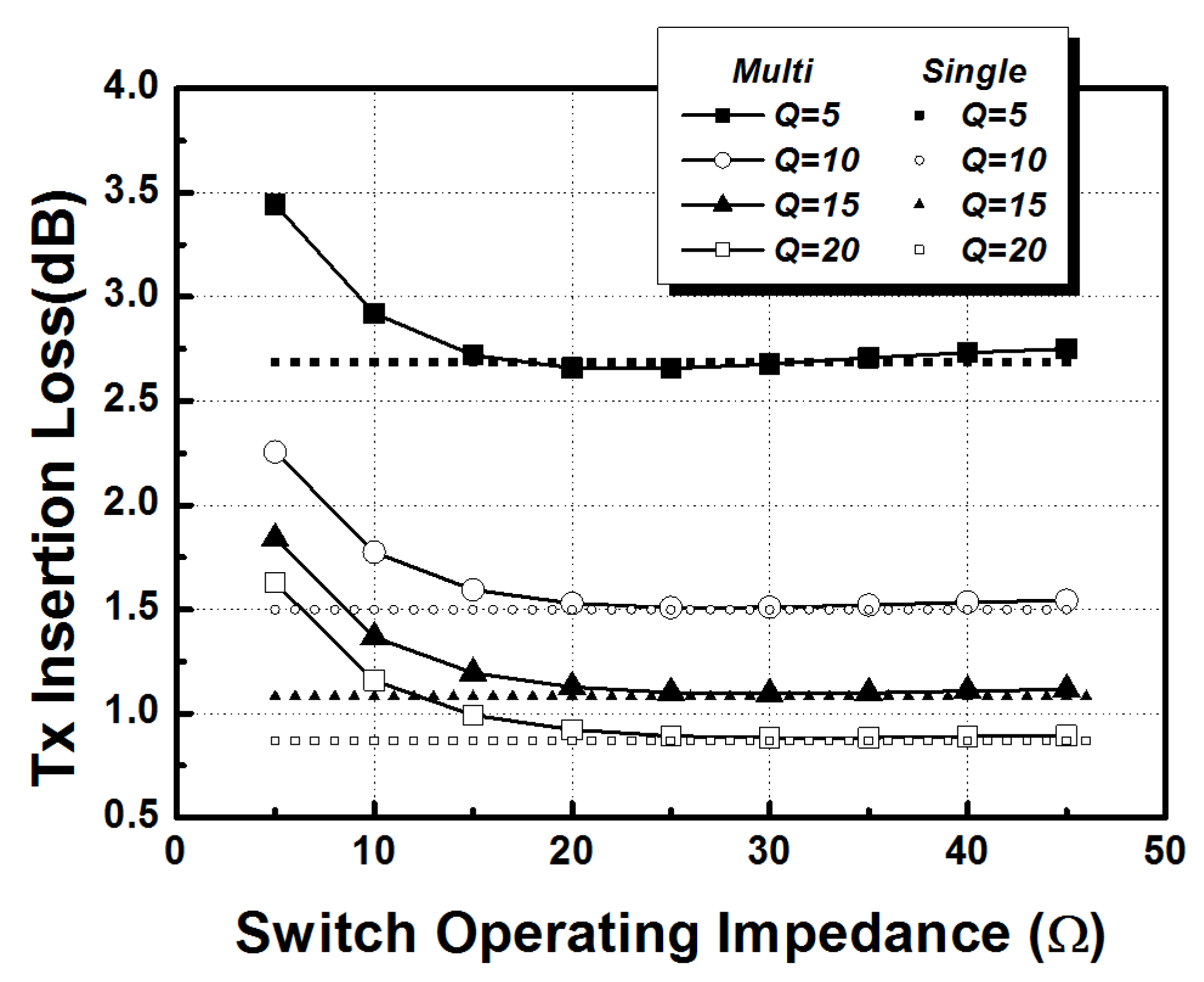
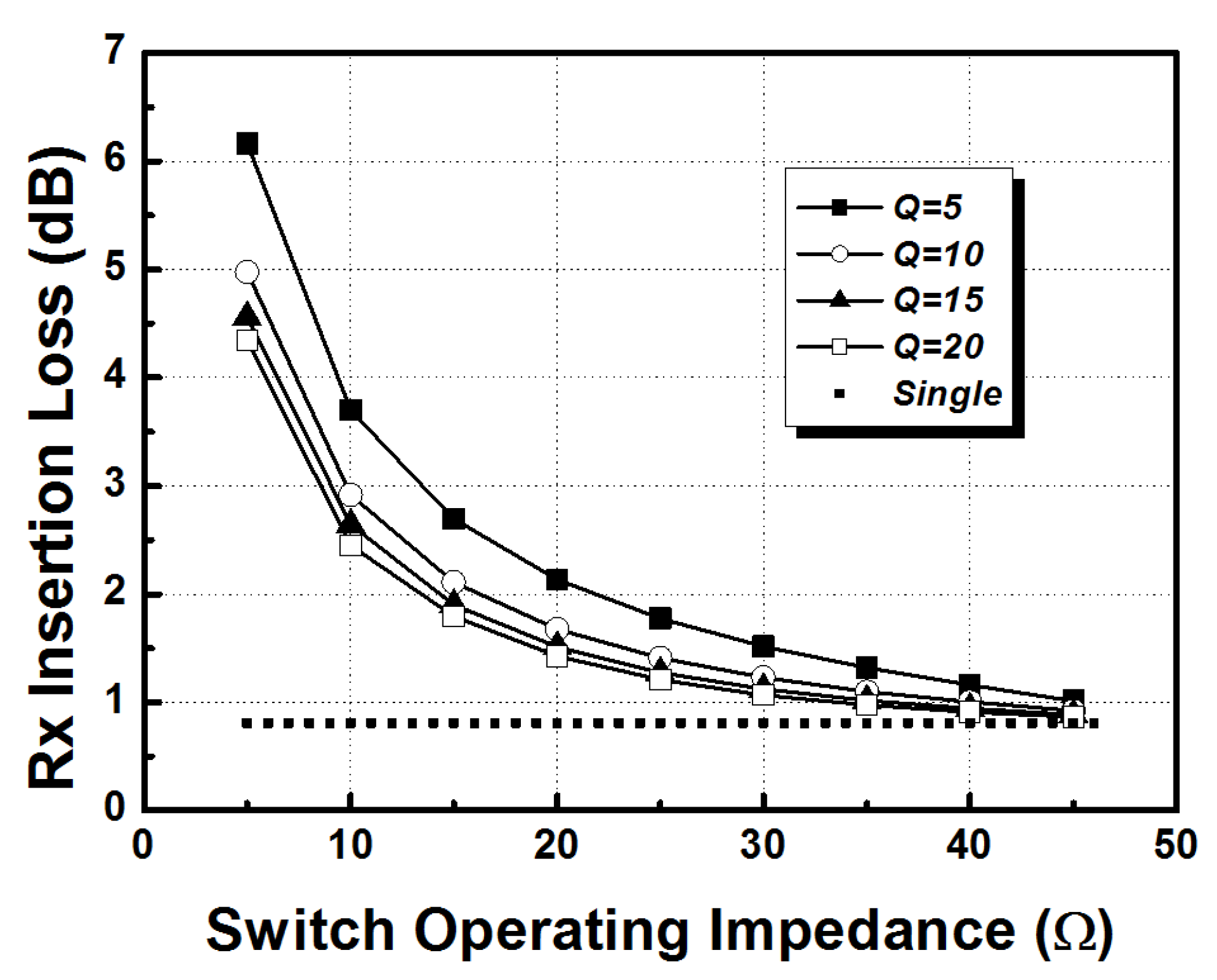
3.2. Switch Insertion Loss

P d i s s = I l o a d 2 R o n + I s u b 2 R s u b  
P o = I l o a d 2 R L 2  
η d i f f s w = P o ,   d i f f P d i s s ,   d i f f + P o ,   d i f f = 2 P o 2 P d i f f + 2 P o = P o P d i f f + P o = R L 2 R o n + 2 R s u b ( ω C r ) 2 ( 1 2 R L + R o n ) 2 1 + ( ω C T R s u b ) 2 + R L  
In the proposed switch design, deep n-well devices are utilized to employ the body floating technique [4]. The cross-sectional view of the deep n-well NMOS switch device is shown in Figure 7. Based on its physical structure, Figure 8a shows the equivalent-circuit model of the device, and four p/n junction diodes are modeled as capacitors. To analyze the insertion loss of the switch device, the model is simplified, as shown in Figure 8b [18]. Assuming that there is no mismatch between two differential signal paths, the efficiency of differential switch is derived by the analysis, and it is represented by Equation (4).
A major factor of the switch insertion loss is the on-resistance of the ON-state switch device. In addition, the loss due to substrate leakage through parasitic capacitors contributes to the total switch loss. Therefore, the width of the switch device is the most important design consideration, balancing the effect of the on-resistance and parasitic coupling effects to achieve the low insertion loss. However, for the proposed structure, there is an additional factor that needs to be considered, since the impedance transformation technique is utilized. It is the load and source impedance seen by the antenna switch. The effect of this factor on the switch insertion loss is analyzed based on equations, as in the previous page.
In this analysis, parasitic capacitances and on-resistance are obtained by simulations, and capacitances between p-well/deep n-well and deep n-well/p-sub were extracted by measurements in the previous work under various p-well and deep n-well bias conditions [18]. P-well and deep n-well ports are biased negatively and positively, respectively, in order to bias the junction diodes reversely. As a result, the loss due to substrate leakage is reduced because the capacitances, Cpwell_DNW and CDNW_psub, become smaller by the biasing. The total capacitance CT in Figure 8b is dominated by these small capacitors, particularly, by CDNW_psub. For the 1.5 mm standard 0.18 µm CMOS device, 0.65 Ω of on-resistance, 80 Ω of Rsub, and 0.15 pF of CT have been used for the analysis. The insertion loss of the antenna switch is expressed by the reciprocal of the magnitude square of S21 which is equal to the derived efficiency in Equation (4). It is converted to dB scale in Figure 9, and the result is well matched to the simulation result. As expected before, the insertion loss of the switch is degraded with the low switch operating impedance, especially with the excessively low impedance.

3.3. Total Loss

The dominating factor in selecting the optimum switch operating impedance is the total loss, since the power-handling capability of the antenna switch is improved as the switch operating impedance decreases. In Tx mode, the total loss of the antenna switches with a multi-section matching network is maintained until the switch operating impedance goes down to 20 Ω, comparing to the loss of the antenna switch with a single matching (output matching of the PA), as shown in Figure 10. On the other hand, in Rx mode, the total loss is worse than that of the single matching case and degraded monotonously as the switch operating impedance decreases, as demonstrated in Figure 11.
That is because a matching network between the antenna and the switch, which is unnecessary for the antenna switch with a single matching, is additionally implemented, and its loss degrades as the impedance transformation ratio increases. Therefore, the switch operating impedance should be chosen carefully, maintaining the total loss at a reasonable level. In order to minimize the Tx loss and maintain the Rx loss under 1 dB, the impedance cannot go lower than 30 or 35 Ω, assuming that the inductor quality factor is between 10 and 15.
As shown in Figure 10 and Figure 11, Tx/Rx insertion loss has been investigated with a variation of the switch operating impedance, and 35 Ω of RSW is chosen for the T/R switch operating impedance to achieve high-power and highly efficient operation. The first matching network (LC balun) transforms 50 Ω to the target impedance.

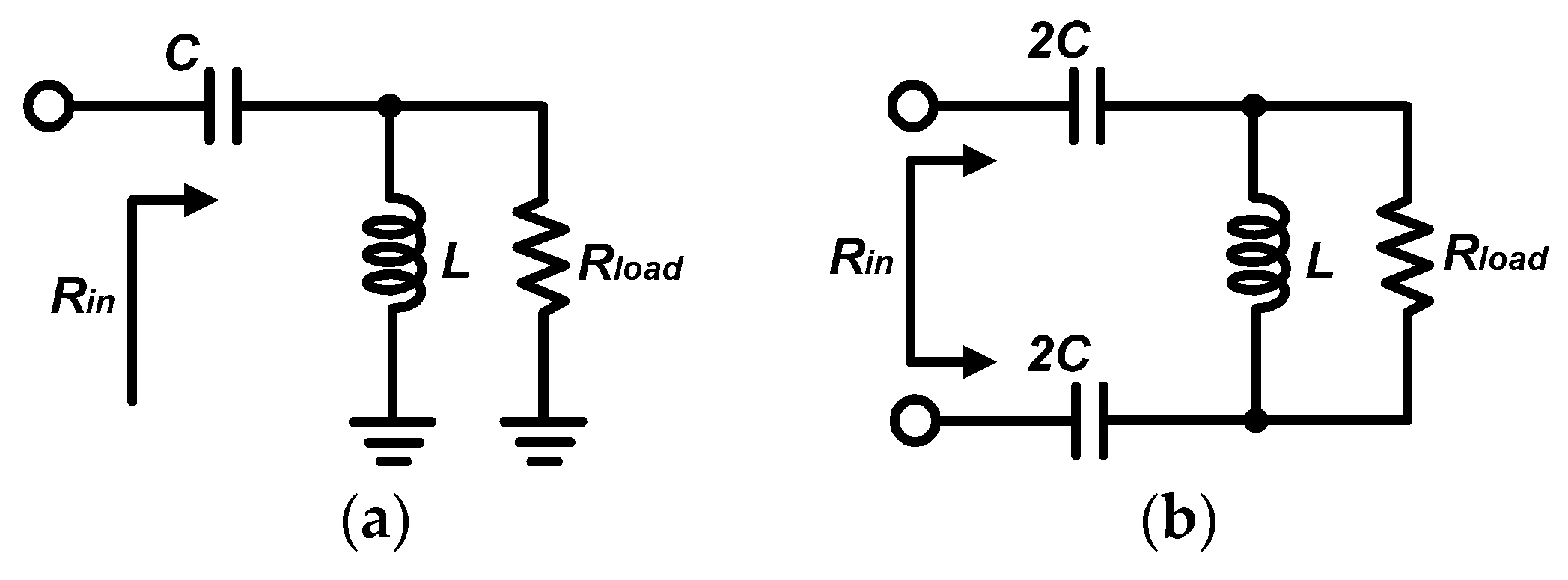
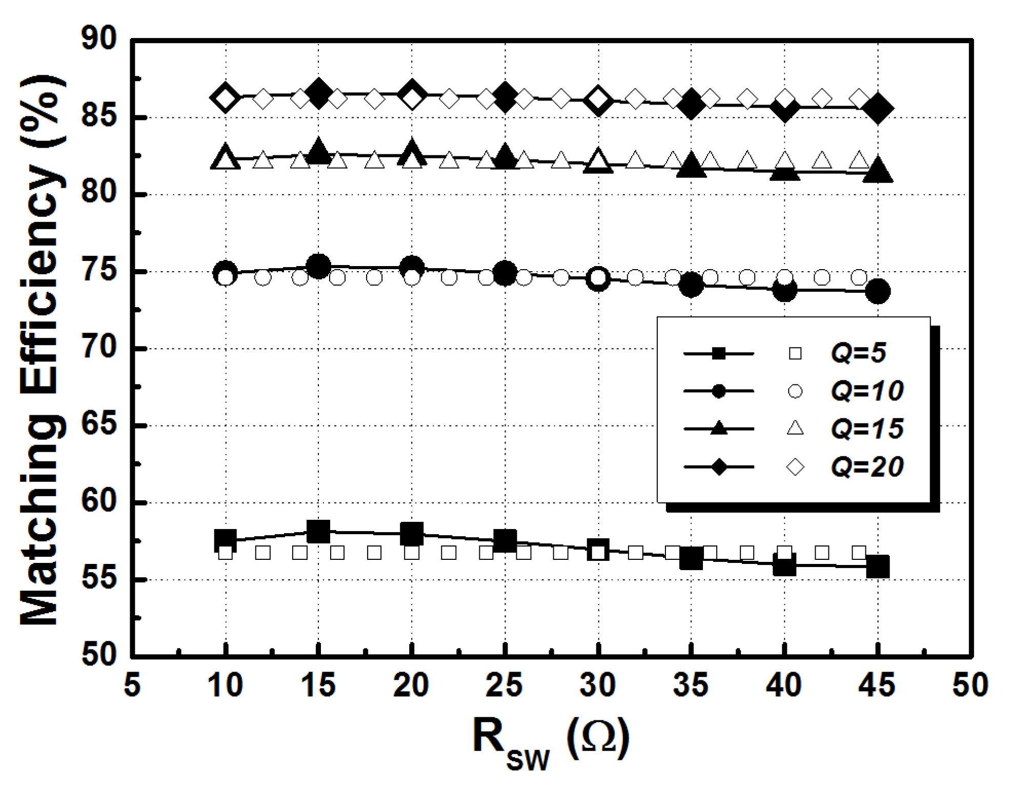
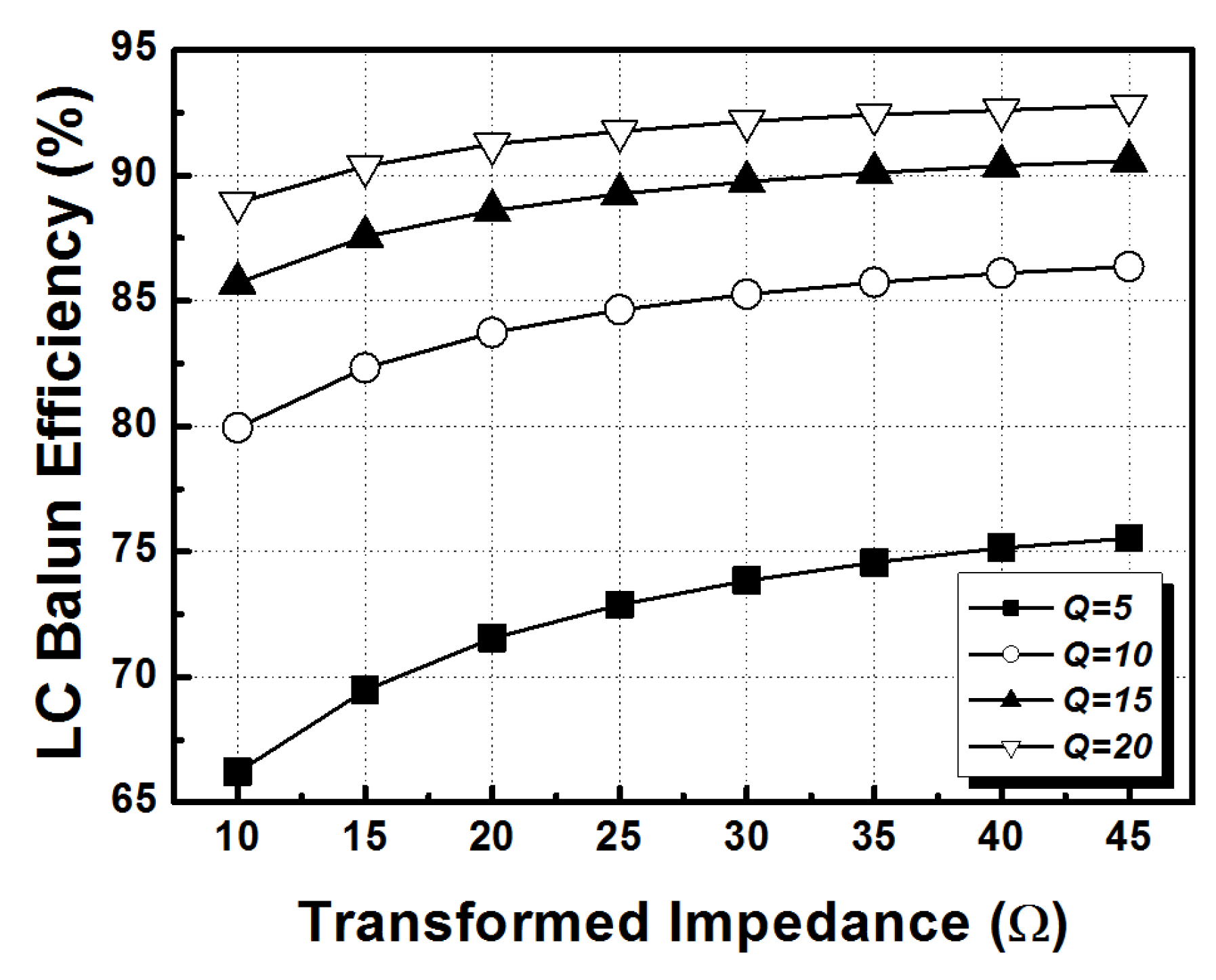
3.4. LC Balun Efficiency

The matching network at the antenna port is designed to obtain a low switch operating impedance for better switch power performance in the proposed design. Since a differential antenna switch is integrated to this matching directly, the matching has to be functioned as a balun, unless a differential antenna is available. Therefore, a lattice-type LC balun is implemented for the matching network. By implementing the LC balun with the differential antenna switch at the antenna port, a fully differential front-end including the PA, an antenna switch, and a low noise amplifier (LNA) can be achieved converting the single-ended antenna port to the differential port. Particularly, in Tx mode, the balun is utilized to combine two differential RF signals at the antenna. The structure of the LC balun is shown in Figure 12 [19]. In order to maximize the output voltage swing at the antenna port, the inductor and capacitor are used in the LC balun, and they resonate at the operating frequency. Their absolute values determine the switch operating impedance, functioning as an impedance matching network. The loss of the LC balun is also analyzed here, and its efficiency is represented by Equation (7), where the Q-factor of inductors is Q = ωL/R, and the impedance transformation ratio is r = RL/RSW = (RL/ωL)2 [20].
P d i s = I 1 2 R + I 3 2 R  
P o = V o 2 R L  
η b a l u n = P o P d i s s + P o 1 1 + 1 2 Q r + 5 r 4 Q 3 + 1 2 Q 2 + r Q  
Based on this equation, efficiencies of the LC balun with different transformation ratio have been plotted in Figure 13 and Figure 14 considering practical inductor Q-factors.

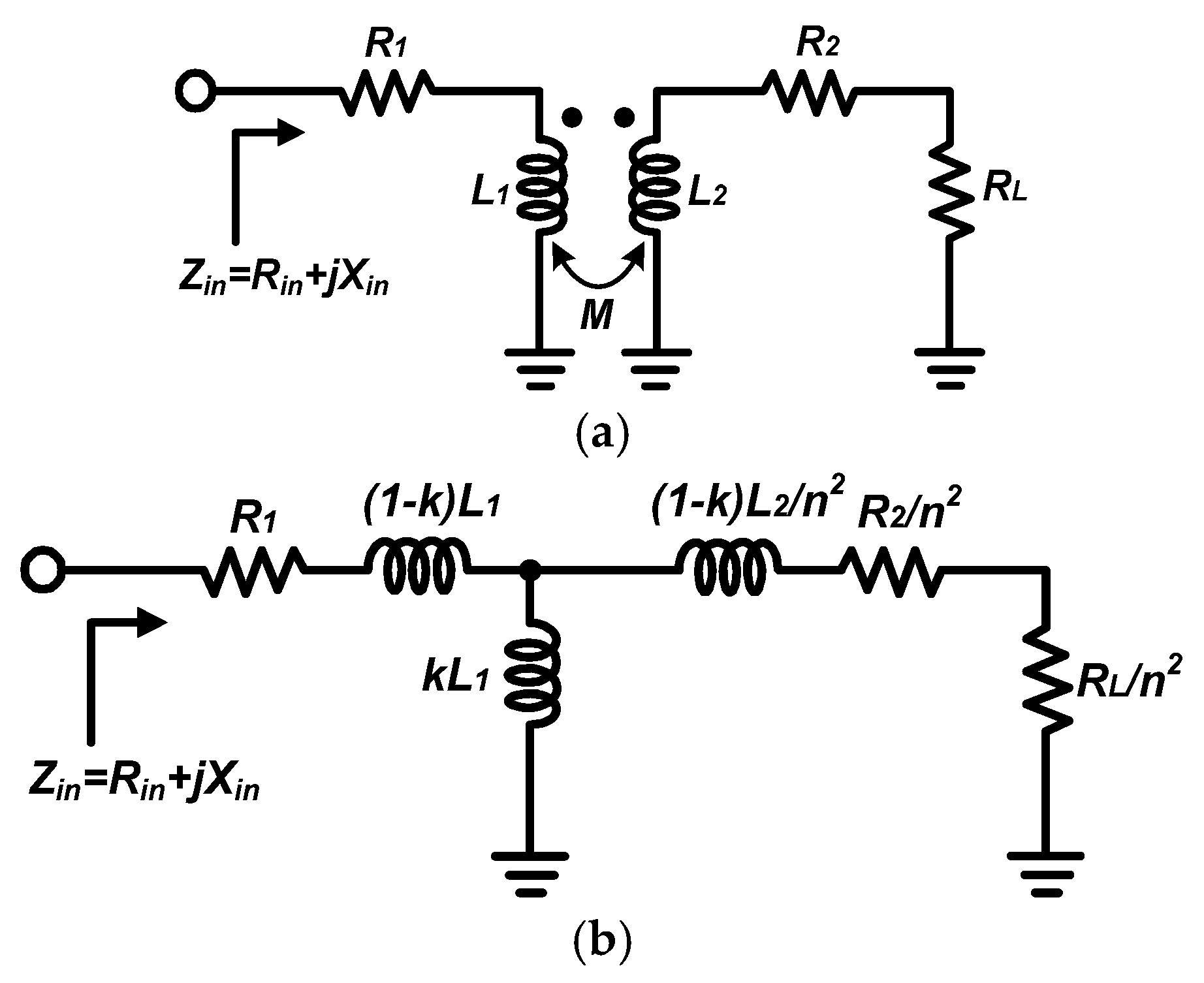
3.5. Transformer Efficiency

For the output matching network of PAs, a transformer is one of the strongest candidates especially for the PAs with Watt-level output power. To generate high output power, the output impedance of the PA is required to be low. Hence, the loss of the output-matching network of the PA is usually high with the large impedance transformation ratio.
R i n = R 1 + ω 2 n 2 k 2 L 1 2 ( R 2 + R L ) ( R 2 + R L ) 2 + ( ω n 2 L 1 ) 2  
P R 1 = R 1 R i n P i n  
P R 2 = ( ω n 2 k L 1 ) 2 ( R 2 + R 1 ) 2 + ( ω n 2 L 1 ) 2 · ( R 2 n 2 ) R i n P i n  
P L = ( ω n 2 k L 1 ) 2 ( R 2 + R L ) 2 + ( ω n 2 L 1 ) 2 · ( R L n 2 ) R i n P i n  
η x f m r = P L P i n = P L P R 1 + P R 2 + P L = 1 1 + 1 R L · ω n 2 L 1 Q 2 + ω L 1 Q 1 R L · ( ω n 2 L 1 ) 2 + R L ( ω n 2 L 1 Q 2 + R L ) ( ω n k L 1 ) 2 2  
Moreover, the unit PA cell has a limitation in generating high output power. Therefore, multiple PAs are connected in parallel to generate high output power. These multiple output powers should be combined effectively, and a transformer is a suitable solution by virtue of its compact power combining capability. Even though LC networks are used as the matching network as well, they are not effective, as the number of segments increases.
Figure 15a shows a 1:n transformer, and the transformer is modeled by the equivalent T-model, as shown in Figure 15b for the efficiency analysis. From the T-model analysis, the efficiency is influenced by various parameters, such as Q-factors of inductor windings, turn ratio (n), and the coupling coefficient (k). Q-factors of primary and secondary winding, Q1 and Q2, are defined by inductances of windings, L1 and L2, and parasitic resistances of the windings, R1 and R2. The coupling coefficient k is related to mutual inductance M and inductances of primary/secondary windings by equation to validate this T-model simplification. In addition, there is one more assumption in this analysis. To analyze the efficiency of the transformer only, tuning capacitors to optimize the matching and loss are not included. From this model, Rin is derived to define the impedance transformation ratio r, Rload/Rin, and total efficiency is solved by circuit analysis in the previous page. As obtained from previous work [21], Rin, and η are represented by Equations (8) and (12), respectively. PR1, PR2, and PL represent dissipated power due to R1, R2, and delivered power to load, respectively. As shown in Figure 16a, a fixed load impedance is transformed to lower Rin, as the turn ratio increases, generating high output power. However, Figure 16b,c show that the efficiency of the transformer is worsened by the increased turn ratio, resulting in the high impedance transformation ratio.
In sum, a high turn ratio is demanded to generate a high power, and it causes the loss degradation. For the proposed structure, the required low Rin can be obtained with a relatively small turn ratio by reducing the switch operating impedance. Therefore, the efficiency of the transformer can be enhanced as the impedance decreases.
As presented in this section, we have analyzed the multi-section matching loss and the switch insertion loss. Based on these two analyses, we present the total loss of the transmitter and the receiver in Section 3.3. From these results, the multi-section matching network will increase the linear power of the transmitter by improving the switch power-handling capability while maintaining the loss, which is similar to or improved compared with the loss of the single section matching for the transmitter. For the receiver, the loss would be degraded slightly for the multi-section matching case, but by choosing the switch operation impedance carefully, we can maintain the total loss at a reasonable level.
Followed by these analyses, we present the loss analysis in actual implementation, which includes LC balun and transformer loss analysis depending on the impedance transformation ratio and target impedance. Through these analyses, it is determined that the loss of the single section matching with a higher transformation ratio would be severely degraded.
Therefore, we conclude that by choosing the optimized switch operation impedance, the multi-section matching network is a comparable or better choice than the single matching network in terms of loss, giving a significant advantage on power handling capability (higher linear pout) for the fully integrated CMOS transmitter.

4. Design and Implementations

A high-power T/R switch with a differential configuration using the multi-section impedance transformation technique is designed in a standard 0.18 µm CMOS process. The proposed circuit is shown in Figure 17, consisting of two matching networks and a differential antenna switch. By implementing the multi-section impedance matching network, the low output impedance of the PA is transformed to 50 Ω gradually, with two steps, optimizing the total loss of the whole signal path. Furthermore, the switch operating impedance can be controlled to enhance the power-handling capability of the antenna switch.
In designing the antenna switch, the typical series–shunt switch structure is chosen. Signal flow through the series switch devices and the shunt switch helps to improve the isolation for both modes. Multiple devices are stacked for the switches, which are OFF-state in Tx mode, to sustain the large signal from the transmitter. In addition, those devices are implemented by using thick-gate-oxide devices to avoid the breakdown. The body floating technique is utilized by implementing deep n-well switch devices [4]. In order to bias junction diodes reversely, p-well ports are biased at negative supply, and deep n-well ports are biased at positive supply through large resistors. Lastly, gates of switch devices are biased through large resistors as well to achieve high AC isolations. Considering the balance between the on-resistance and the parasitic capacitance of switch devices, gate widths have been chosen as 1.5 mm for the Tx series switch, 1.2 mm for the Rx series switch, 600 μm for the Tx shunt switch, and 200 μm for the Rx shunt switch. In order to endure the high voltage swing, four switch devices have been stacked on the Tx shunt arm, and two switch devices have been stacked on the Rx series arm. The Tx series switch and Rx series switch were not stacked to minimize Tx insertion loss and improve Rx isolation.
For the PA design details, the gate widths of both common source (CS) and common gate (CG) devices are 4 mm for each differential pair, which consists of 64 unit cells. Each unit cell has 8 fingers with 8 μm width/finger (8 μm × 8 finger × 64 cells). To minimize the Miller effect, 2.5 pF of cross-neutralized capacitors (Cxnp and Cxnn) are utilized, while 500 Ω of resistors and 0.5 pF of capacitors are employed for the feedback network. The optimal load impedance was obtained from the load-pull simulation as 5.5 + j9 Ω at which the individual core can deliver more than 30 dBm output power with the maximum efficiency. From the switch operating impedance, we designed the output transformer to match the PA optimal load impedance. By doing so, we could optimize the PA performance as well as an integrated PA and switch module performance.
The transformer combines the outputs of two identical single-ended switches. An LC balun is implemented at the antenna side. To obtain accurate inductances, inductor layouts are done with the electromagnetic (EM) simulations, considering parasitic inductances of metal lines. Bonding wire inductances to the ground are also considered. An inductor and a capacitor in series in the LC balun are designed to be resonated at 1.9 GHz, and the values of the shunt inductor and capacitor are carefully tuned to obtain 35 Ω of the switch operating impedance from the EM simulations. Q-factors of inductors used in the LC balun are in the range of 15–20 at 1.9 GHz.
For the other matching network, the transformer, which can be used as an output matching network of the PA, is implemented. The efficiency of the transformer is optimized by including capacitors at the input and output ports of the transformer in parallel. To improve the efficiency of the transformer further, the width of primary winding is expanded twice. In order to mitigate the proximity effect, the expanded winding is split in half, and the secondary winding is located in the middle of it. With this layout, the resistance of the primary winding is reduced and the current crowding is avoided, resulting in enhancement in passive efficiency. To obtain high Q-factors for both primary and secondary windings, thick metal layers, copper and alumina, are stacked. The widths of windings and the gap between them are determined from EM simulations, maximizing the transformer efficiency, and the values are set by 30 μm and 5 µm, respectively. The simulated maximum available gain of the transformer is shown in Figure 18.
It shows that the efficiency of the transformer is enhanced with the differential architecture because the Q-factor of the inductors used in the transformer is higher when it operates in a differential mode than in a single-ended mode. In the proposed structure, the transformer can be operated in a differential mode because a differential antenna switch is integrated to the output of the transformer, and the other matching network functions as a balun.

5. Measurement Results

The proposed transmitter front-end module is fabricated in a standard 0.18 µm CMOS process, and the microphotograph is shown in Figure 19. The total size including wire-bonding pads is 2500 μm × 1100 μm. This proposed structure consists of two-pairs of power amplifiers with a cascode structure, a high-power differential switch, a multi-section impedance matching network with a transformer, an LC balun, and an integrated negative voltage generator. An LC balun has been designed to provide 35 Ω of the switch operating impedance.
As shown in Figure 20a, the output power is quite flat over the frequency, and it is measured as 32.1 dBm at 1.9 GHz, which is the highest value among the works presented so far. For the efficiency of the PA, since the second matching network is implemented with an LC balun, the efficiency is varied across band slightly, and it is 38.3% at the target frequency.
Figure 20b shows the measured first harmonics over the frequency. The proposed transmitter module presents the low harmonic power over the frequency, and it is another advantage of the proposed technique. Since both the PA and the switch are implemented differentially, the second harmonic is very low especially. The measured second and third harmonics are not over 52 dBc across the band.
The measured comparison between the proposed design and the conventional design is shown in Figure 21. The proposed module includes a fully differential PA and a switch with the multi-section PA output matching, while the conventional module consists of a single-ended switch and one PA output matching. As shown in Figure 21, the proposed transmitter front-end module shows the better peak efficiency when it is compared to that of the conventional counterpart, since the single-ended switch is not enough to handle the high power. As expected, it is measured that the peak output power and the gain at the high-power region are degraded in a conventional case, too.
To validate this proposed design, the P1dB of the stand-alone differential switch and the Rx insertion loss of switch are measured as well. The measured P1dB of the proposed switch is well above 33.5 dBm across the measured frequency band, as shown in Figure 22a. Its Rx loss level remains at a reasonable level, 1.6 dB at 1900 MHz, as shown in Figure 22b.

6. Discussion

In this paper, a high-power and highly efficient fully integrated CMOS transmitter front-end module is presented. The power-handling capability of the module is improved with the differential T/R switch structure and the multi-section impedance transformation technique. By utilizing the multi-section output impedance matching, the efficiency of the module is enhanced with the proper RSW. According to the analyses, 35 Ω of RSW is chosen for the T/R switch operating impedance for high-power and highly efficient operation. The proposed module also includes the CMOS T/R switch controller, which includes an oscillator, a charge pump, and two-level shifters. The module transmits 32.1 dBm of output power to antenna, with the 38.3% of PAE. As shown in the Table 1, this work shows the best performance among the CMOS implementations, and it is comparable to the GaAs counterpart.

Author Contributions

Conceptualization, H.-W.K., M.A., O.L. and C.-H.L.; methodology, H.-W.K., H.K. (Hyungwook Kim) and O.L.; validation., H.-W.K., H.K. (Hyoungsoo Kim) and O.L.; data curation, H.-W.K.; writing—original draft preparation, H.-W.K.; writing—review and editing, H.-W.K., H.K. (Hyoungsoo Kim) and O.L. All authors have read and agreed to the published version of the manuscript.

Funding

This work was supported by the National Research Foundation of Korea (NRF) grant funded by the Korea government (MSIT) (NRF2020R1A2B5B01001508).

Conflicts of Interest

The authors declare no conflict of interest.

References

  1. Abidi, A.A. RF CMOS comes of age. IEEE J. Solid-State Circuits 2004, 39, 549–561. [Google Scholar] [CrossRef]
  2. Ohnakado, T.; Yamakawa, S.; Murakami, T.; Furukawa, A.; Taniguchi, E.; Ueda, H.; Suematsu, N.; Oomori, T. 21.5-dBm power-handling 5-GHz transmit/receive CMOS switch realized by voltage division effect of stacked transistor configuration with depletion-layer-extended transistors (DETs). IEEE J. Solid-State Circuits 2004, 39, 577–584. [Google Scholar] [CrossRef]
  3. Talwalkar, N.A.; Yue, C.P.; Gan, H.; Wong, S.S. Integrated CMOS transmit-receive switch using LC-tuned substrate bias for 2.4-GHz and 5.2-GHz applications. IEEE J. Solid-State Circuits 2004, 39, 863–8702004. [Google Scholar] [CrossRef]
  4. Yeh, M.-C.; Tsai, Z.-M.; Liu, R.-C.; Lin, K.-Y.; Chang, Y.-T.; Wang, H. Design and analysis for a miniature CMOS SPDT switch using body-floating technique to improve power performance. IEEE Trans. Microw. Theory Tech. 2006, 54, 31–39. [Google Scholar]
  5. Huang, F.-J.; Kenneth, K.O. Single-pole double-throw CMOS switches for 900-MHz and 2.4-GHz applications on p-silicon substrates. IEEE J. Solid-State Circuits 2004, 39, 35–41. [Google Scholar] [CrossRef]
  6. Li, Q.; Zhang, Y.P. CMOS T/R switch design: Towards ultra-wideband and high frequency. IEEE J. Solid-State Circuits 2007, 42, 563–570. [Google Scholar] [CrossRef]
  7. Kidwai, A.A.; Fu, C.-T.; Jenson, J.C.; Taylor, S.S. A fully integrated ultra-low insertion loss T/R switch for 802.11b/g/n application in 90nm CMOS process. IEEE J. Solid-State Circuits 2009, 44, 1352–1360. [Google Scholar] [CrossRef]
  8. Xu, H.; Kenneth, K.O. A 31.3-dBm bulk CMOS T/R switch using stacked transistors with sub-design-rule channel length in floated p-wells. IEEE J. Solid-State Circuits 2007, 42, 2528–2534. [Google Scholar] [CrossRef]
  9. Costa, J.; Carroll, M.; Jorgenson, J.; Mckay, T.; Ivanov, T.; Dinh, T.; Kozuch, D.; Remoundos, G.; Kerr, D.; Tombak, A.; et al. A silicon RFCMOS SOI technology for integrated cellular/WLAN RF TX modules. In Proceedings of the IEEE MTT-S International Microwave Symposium, Honolulu, HI, USA, 3–8 June 2007; pp. 445–448. [Google Scholar]
  10. Carroll, M.; Kerr, D.; Iversen, C.; Tombak, A.; Pierres, J.-B.; Mason, P.; Costa, J. High-resistivity SOI CMOS cellular antenna switches. In Proceedings of the IEEE Compound Semiconductor Integrated Circuit Symposium, Greensboro, NC, USA, 11–14 October 2009; pp. 1–4. [Google Scholar]
  11. Miyatsuji, K.; Ueda, D. A GaAs high power RF single-pole dual throw switch IC for digital-mobile communication system. IEEE J. Solid-State Circuits 1995, 30, 979–983. [Google Scholar] [CrossRef]
  12. Numata, K.; Takahashi, Y.; Maeda, T.; Hida, H. A +2.4/0V controlled high power GaAs SPDT antenna switch IC for GSM application. In Proceedings of the 2002 IEEE Radio Frequency Integrated Circuits (RFIC) Symposium. Digest of Papers (Cat. No.02CH37280), Seattle, WA, USA, 3–4 June 2002; pp. 141–144. [Google Scholar]
  13. Aoki, I.; Kee, S.D.; Rutledge, D.B.; Hajimiri, A. Fully integrated CMOS power amplifier design using the distributed active-transformer architecture. IEEE J. Solid-State Circuits 2002, 37, 371–383. [Google Scholar] [CrossRef] [Green Version]
  14. An, K.H.; Lee, O.; Kim, H.; Lee, D.H.; Han, J.; Yang, K.S.; Kim, Y.; Chang, J.J.; Woo, W.; Lee, C.-H.; et al. Power-combining transformer techniques for fully-integrated CMOS power amplifiers. IEEE J. Solid-State Circuits 2008, 43, 1064–1075. [Google Scholar] [CrossRef]
  15. Kim, H.-W.; Ahn, M.; Lee, O.; Kim, H.; Kim, Y.Y.H.S.; Lee, C.-H.; Laskar, J. Design and Analysis of CMOS T/R Switches with the Impedance Transformation Technique. IEEE Microw. Wirel. Compon. Lett. 2017, 27, 1137–1139. [Google Scholar] [CrossRef]
  16. Kim, H.-W.; Ahn, M.; Lee, O.; Lee, C.-H.; Laskar, J. A high power CMOS differential T/R switch using multi-section impedance transformation technique. In Proceedings of the 2010 IEEE Radio Frequency Integrated Circuits Symposium, Anaheim, CA, USA, 23–25 May 2010; pp. 483–486. [Google Scholar]
  17. Aoki, I.; Kee, S.D.; Rutledge, D.B.; Hajimiri, A. Distributed active transformer—A new power-combining and impedance-transformation technique. IEEE Trans. Microw. Theory Tech. 2002, 50, 316–331. [Google Scholar] [CrossRef] [Green Version]
  18. Huang, F.-J.; Kenneth, K.O. A 0.5-µm CMOS T/R switch for 900-MHz wireless applications. IEEE J. Solid-State Circuits 2001, 36, 486–492. [Google Scholar] [CrossRef]
  19. Ahn, M.; Kim, H.-W.; Lee, C.-H.; Laskar, J. A 1.8-GHz 33-dBm P0.1-dB CMOS T/R switch using stacked FETs witch feed-forward capacitors in a floated well structure. IEEE Trans. Microw. Theory Tech. 2009, 57, 2261–2670. [Google Scholar]
  20. Reynaert, P.; Steyaert, M. A 2.45-GHz 0.13-µm CMOS PA with parallel amplification. IEEE J. Solid-State Circuits 2007, 42, 551–562. [Google Scholar] [CrossRef]
  21. Lee, O.; An, K.H.; Kim, H.; Lee, D.H.; Han, J.; Yang, K.S.; Lee, C.-H.; Kim, H.; Laskar, J. Analysis and design of fully integrated high-power parallel-circuit class-E CMOS power amplifiers. IEEE Trans. Circuits Syst. I Reg. Papers 2010, 57, 725–734. [Google Scholar] [CrossRef]
  22. DiCarlo, P.; Boerman, S.; Burton, R.; Chung, H.-C.; Evans, D.; Gerard, M.; Gering, J.; Khayo, I.; Lagrandier, L.; Lalicevic, I.; et al. A highly integrated quad-band GSM TX-front-end-module. In Proceedings of the 25th Annual Technical Digest 2003. IEEE Gallium Arsenide Integrated Circuit (GaAs IC) Symposium, 2003, San Diego, CA, USA, 9–12 November 2003; pp. 280–283. [Google Scholar]
  23. De Graauw, A.J.M.; van Bezooijen, A.; Chanlo, C.; den Dekker, A.; Dijkhuis, J.; Pramm, S.; ten Dolle, H.K.J. Miniaturized quad-band front-end module for GSM using Si BiCMOS and passive integration technologies. In Proceedings of the IEEE Bipolar/BiCMOS Circuits and Technology Meeting (BCTM), Maastricht, The Netherlands, 8–10 October 2006; pp. 1–4. [Google Scholar]
  24. Jeon, J.; Kuhn, W.B. A UHF CMOS transceiver front-end with a resonant TR switch. In Proceedings of the IEEE Radio and Wireless Symposium (RWS), Long Beach, CA, USA, 9–11 January 2007; pp. 71–74. [Google Scholar]
  25. Ahn, M.; An, K.H.; Lee, C.; Laskar, J.; Kim, H. Fully integrated high-power RF front-end circuits in 2 GHz using 0.18μm standard CMOS process. In Proceedings of the IEEE Asia-Pacific Microwave Conference (APMC), Hong Kong, China, 16–20 December 2008; pp. 1–4. [Google Scholar]
Figure 1. Block diagram of transmitter front-end. (a) Conventional structure with a single-ended switch. (b) Proposed structure with a differential switch employing impedance transformation technique.
Electronics 10 01028 g001aElectronics 10 01028 g001b
Figure 2. Simulated voltage swing over each single-ended switch (vacant symbols are for path1, and solid symbols are for path2, 33 dBm of input power is applied at 1.9 GHz).
Electronics 10 01028 g002
Figure 3. Simulated P−0.1dB of antenna switches (control voltages are 3 V/2 V and the switches operate at 1.9 GHz).
Electronics 10 01028 g003
Figure 4. Simple LC-type impedance matching networks. (a) Single-ended. (b) Differential.
Electronics 10 01028 g004
Figure 5. Impedance matching networks from output of the PA to antenna. (a) Multi-section matching. (b) Single-section matching.
Electronics 10 01028 g005
Figure 6. Efficiencies of impedance matching networks. Solid symbols and vacant symbols represent efficiencies of multi-section and single-section matching, respectively.
Electronics 10 01028 g006
Figure 7. Cross-sectional view of an NMOS transistor in a deep n-well.
Electronics 10 01028 g007
Figure 8. (a) Equivalent circuit model of deep n-well switch devices including substrate junction diodes. (b) Simplified equivalent circuit model for analysis.
Electronics 10 01028 g008
Figure 9. Insertion loss of a single switch device versus switch operating impedances.
Electronics 10 01028 g009
Figure 10. Total loss of the antenna switches with a multi-section (scatter and line) and single-section (scatter) matching network in Tx mode.
Electronics 10 01028 g010
Figure 11. Total loss of the antenna switch with multi (scatter and line) and single-section (scatter) matching network in Rx mode.
Electronics 10 01028 g011
Figure 12. The schematic of an LC balun.
Electronics 10 01028 g012
Figure 13. Efficiency of an LC-type matching (differential-in and differential-out). Q represents the quality factor of the inductor used in the network.
Electronics 10 01028 g013
Figure 14. Efficiency of an LC balun (differential-in and single-out).
Electronics 10 01028 g014
Figure 15. (a) Transformer model. (b) Transformer equivalent T-model.
Electronics 10 01028 g015
Figure 16. (a) Rin vs. turn ratio and impedance transform ratio vs. turn ratio. (b) Transformation efficiency vs. turn ratio. (c) Transformation efficiency vs. impedance transformation ratio.
Electronics 10 01028 g016
Figure 17. The schematic of the proposed fully integrated differential switch and power amplifier in CMOS technology.
Electronics 10 01028 g017
Figure 18. Simulated transformer maximum gain for single-ended and differential cases.
Electronics 10 01028 g018
Figure 19. Microphotograph of the proposed structure.
Electronics 10 01028 g019
Figure 20. Measurement results. (a) Output power and PAE vs. frequency. (b) Harmonics vs. frequency.
Electronics 10 01028 g020
Figure 21. Compared measurement results of output power and PAE over various input power.
Electronics 10 01028 g021
Figure 22. Measurement results of (a) P1dB of the differential switch and (b) Rx insertion loss of the switch.
Electronics 10 01028 g022
Table 1. Transmitter front-end performance summary.
ProcessFreq.FeaturesSupply Volt.Pout (dBm)/
PAE
[22]GaAs/
pHEMT
900 MHzpHEMT switch5 VPOUT: 34
PAE: 45%
[23]BiCMOS870 MHzpHEMT switch3.5 VPOUT: 32
PAE: 35%
[24]CMOS SOI400 MHzResonant switch
UHF application
3.3 VPOUT: 29
PAE: 29%
[25]0.18 µm CMOS2 GHzTransistor stacking
LNA design included
3.3 VPOUT: 29.7
PAE:
35%
This work0.18 µm CMOS1.9 GHzDiff. topology
Multi-sect.
Impedance matching
3.3 VPOUT: 32.1
PAE: 38.3%
Publisher’s Note: MDPI stays neutral with regard to jurisdictional claims in published maps and institutional affiliations.

