Article

Output Voltage Imbalance Compensation Using dc Offset Voltage for Split dc-Link Capacitor 3-Leg Inverter

1
Energy Conversion Research Centre, Korea Electronics Technology Institute, Gwangju 61011, Korea
2
Department of Electrical Engineering, Chonnam National University, Gwangju 61186, Korea
3
Department of Electronic Engineering, Hanbat National University, Daejeon 34158, Korea
*
Author to whom correspondence should be addressed.
Electronics 2021, 10(9), 1029; https://doi.org/10.3390/electronics10091029
Submission received: 18 March 2021 / Revised: 18 April 2021 / Accepted: 24 April 2021 / Published: 26 April 2021
(This article belongs to the Section Power Electronics)

Abstract

:
In this paper, we analyzed the output voltage imbalance and the cause of the offset voltage in 3-phase 3-leg inverters by using Millman’s theory. Based on this result, we proposed a voltage imbalance compensation algorithm using the dc offset voltage that appeared at the neutral point voltage of the load. To apply the proposed imbalance compensation algorithm, it needs a circuit structure of 3-phase 4-wire such as split dc-link capacitor 3-leg inverter and 4-leg inverter. Therefore, the total harmonic distortion (THD) of the load phase current according to the imbalance rate of the load was analyzed for the two inverters. Then, PSIM simulation and experiments based on a 10 kW-prototype of split dc-link capacitor 3-leg inverter were implemented to verify the validity of the proposed imbalance compensation algorithm.

1. Introduction

The 3-phase 4-wire inverter has a split capacitor 3-leg inverter that connects the midpoints of the series-connected dc-link capacitors to the neutral point of the grid or load, and a 4-leg inverter that adds one more leg to the 3-leg inverter to connect the neutral point. The split capacitor 3-leg inverter can reduce the imbalance rate by allowing the neutral line current to flow to the neutral point of split dc-link capacitors and is easy to implement, using sinusoidal pulse width modulation (SPWM). However, as the imbalance rate of the load increases, the current flowing to the neutral line increases, which occurs a voltage imbalance problem at the dc-link stage. As a result, it causes problems such as imbalance of output voltage and increased voltage distortions [1,2,3,4,5,6,7,8]. The 4-leg inverter can be applied with the space vector pulse width modulation (SVPWM) algorithm even if a leg is added, which makes switching control easy and the dc-link voltage utilization ratio high [9,10,11,12,13,14]. In addition, the added leg can be used to fully control the current of the neutral line, making it easy to compensate for the imbalance of the grid and an excellent response to imbalance loads in the independent operation (islanding operation or stand-alone operation) mode [15,16,17,18,19,20,21,22,23,24,25,26,27,28,29,30,31]. It also has the advantage of obtaining high reliability with the redundancy effect [28]. Therefore, the most appropriate method is to use a 4-leg inverter to improve the imbalance rate that occurs in the grid. However, to use the 4-leg inverter, there is only a way to replace the previously installed power conditioning system (PCS) employing a 3-phase 3-leg inverter, which is as expensive as a new installation.
To improve the grid imbalance, in terms of cost-to-change, a structure that can improve the imbalance rate by utilizing the previously installed PCS is advantageous. The 3-leg inverter can be changed to a 3-leg inverter structure with a split dc-link capacitor that can compensate for voltage imbalance by connecting the neutral point of the split dc-link capacitors and the neutral point of the 3-phase load. Therefore, despite the disadvantages of 3-leg inverters with split dc-link capacitors, it is an economical method that can be applied to preinstalled 3-phase 3-leg inverters.
In this paper, we first analyzed the causes of output voltage imbalance of a 3-leg inverter using Millman’s theorem. Based on this result, we proposed an inverter output voltage imbalance compensation algorithm using dc offset voltage that appeared at the neutral point of the load. We analyzed the relationship between the imbalance rate and total harmonic distortion (THD) for 3-phase 4-wire inverters required for applying the proposed offset voltage compensation algorithm through PSIM simulation. We modified the structure of the preinstalled 3-leg inverter into a split-dc link capacitor 3-leg inverter and validated the validity of the proposed imbalance voltage compensation algorithm through experiments.

2. Analysis of 3-Leg Inverter Using Millman’s Theory

2.1. Balanced 3-Phase System

The balanced 3-phase system has the same voltage for each phase. This means that the amplitude and phase angle of each phase is the same, which are connected to a symmetric voltage source with a phase difference of 120°. In a balanced 3-phase Y–Y connection, the line current and phase current equal in amplitude and in phase. It is known that the potential difference between the neutral points of the voltage source and the load is zero by Millman’s theory. Then the phase voltage of the load is as follows.
V r N = 2 3 V r 1 3 V s 1 3 V t
V s N = 1 3 V r + 2 3 V s 1 3 V t
V t N = 1 3 V r 1 3 V s + 2 3 V t
Here, VrN is a phase voltage of the r-load, VsN is a phase voltage of the s-load, and VtN is a phase voltage of the t-load in a balanced 3-phase load. Vr is the r-phase voltage, vs. is the s-phase voltage, and Vt is the t-phase voltage in a balanced 3-phase voltage source. In a balanced 3-phase condition, it can be seen that the phase voltage of the load is only affected by the amplitude of the source voltage of each phase.

2.2. Unbalanced 3-Phase System

When imbalance occurs between the phase voltages of the source, the load shows an unbalanced voltage, and the phase voltage of the source and the load do not match. The voltage between the neutral points is as follows:
v N n = V r Z r + V s Z s + V t Z t 1 Z r + 1 Z s + 1 Z t = 1 3 ( V r + V s + V t )
Here, vNn is the voltage between the neutral points of the source and the load. Zx is an impedance of r-, s-, and t-loads. Vx means the phase voltage of the source (the lower subscript x = r, s, t). In other words, when an unbalanced phase voltage is applied to a load, the source voltage on each phase and the voltage on the load do not match, resulting in an ac component at the neutral point. Therefore, if the voltage at the neutral point can be subtracted from the phase voltage of the source, the neutral point voltage can be zero. However, at the neutral point of the Y-connection load, the sum of the currents must be zero by Kirchhoff’s current law (KCL) so that the unbalanced current cannot flow. This means that to improve the imbalance for voltage and current, a current path is required to flow an unbalanced current to the neutral point.

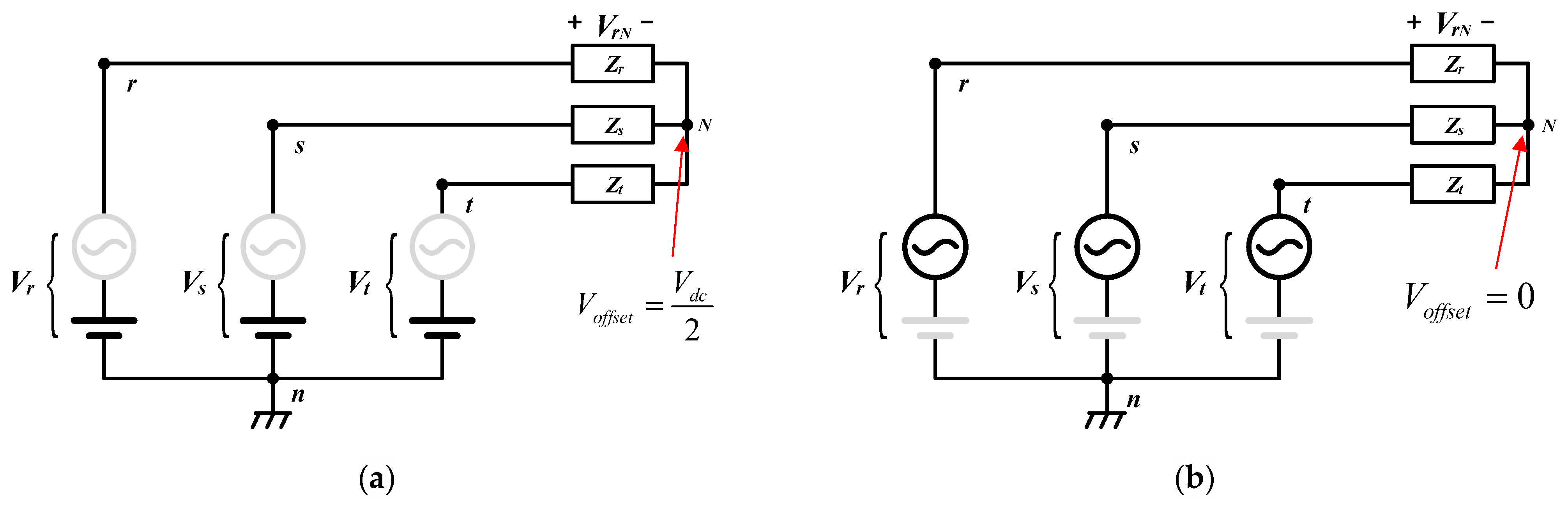
2.3. Offset Voltage in 3-Leg Inverter

Figure 1 shows a circuit configuration of a 3-phase 3-leg inverter. The input voltage of the inverter is one dc voltage source (Vdc), and the output voltage of each leg generates the offset voltage at point n, where the capacitors are series-connected.
Figure 2 shows the equivalent circuit of a 3-leg inverter. Each phase voltage has both ac and dc components and can be interpreted separately. Figure 2a is an equivalent circuit for dc component, and the ac component does not appear at the neutral point of the load as the ac voltage is zero. At this time, a dc voltage appears at the neutral point of the load, which is the same amplitude as Vdc/2. Figure 2b is an equivalent circuit for ac components, and the dc component does not appear at the neutral point because the dc voltage is zero.

2.4. Concept of the Proposed Imbalance Voltage Compensation

In a balanced 3-phase condition, the neutral point voltage is 0 V, so the voltage at the neutral point of the load is also 0 V. Thus, by the theorem of superposition, the voltage at the neutral point of the load is only a dc component. The dc component of the inverter output voltage is the neutral point voltage, which is called the offset voltage (Voffset). Therefore, each leg output voltage of the inverter is as follows:
V r = V o f f s e t + V r sin ( ω t )
V s = V o f f s e t + V s sin ( ω t 2 3 π )
V t = V o f f s e t + V t sin ( ω t + 2 3 π )
Here, Vr is the r-leg voltage, Vs is the s-leg voltage, and Vt is the t-leg voltage of the 3-leg inverter. The upper subscript of the asterisk (*) means the command value. The output voltage of each leg of the inverter changes the utilization ratio of the output voltage according to the offset voltage. Depending on the offset voltage, the output characteristics can be changed without affecting the fundamental component of the output voltage, allowing voltage control over the neutral point voltage of the load.
In 3-leg inverters, the output command of each phase voltage is different, resulting in an unbalanced voltage. If the load is unbalanced, the output voltage of each leg affects the load phase voltage, resulting in a different output command of the phase voltage from the inverter’s output phase voltage. In Figure 1, the relationship between impedance and voltage command for load phase voltages can be expressed by (8)–(10). Here, VrN is a phase voltage of the r-load, VsN is a phase voltage of the s-load, and VtN is a phase voltage of the t-load in a 3-phase load. Vr is the r-leg voltage, Vs is the s-leg voltage, and Vt is the t-leg voltage of the 3-leg inverter. The upper subscript asterisk (*) means the control command value.
V r N = Z r ( Z s + Z t ) Z r Z s + Z s Z t + Z t Z r V r ( Z s + Z t ) Z r Z s + Z s Z t + Z t Z r V s ( Z t + Z r ) Z r Z s + Z s Z t + Z t Z r V t
V s N = ( Z r + Z t ) Z r Z s + Z s Z t + Z t Z r V r + Z s ( Z r + Z t ) Z r Z s + Z s Z t + Z t Z r V s ( Z t + Z s ) Z r Z s + Z s Z t + Z t Z r V t
V t N = ( Z r + Z t ) Z r Z s + Z s Z t + Z t Z r V r ( Z s + Z r ) Z r Z s + Z s Z t + Z t Z r V s + Z t ( Z s + Z r ) Z r Z s + Z s Z t + Z t Z r V t
In the conventional method for the imbalance control of inverters operating in an independent operation mode, the voltage control is performed for each phase to improve the voltage imbalance rate, as shown in Figure 3a. To control the amplitude of voltage, it creates a reference value for each phase and uses a PI (Proportional-Integral) controller for the q-axis value. For coordinate conversion, it uses the q-axis and d-axis values of the output of the controller. When converting coordinates, the value α is equal to the value of the r-, s-, t-phase, so for each axis, the value of the coordinate transformation value is transferred to the SVPWM module to control the output voltage of the inverter [30,31].
On the other hand, the proposed method performs a coordinate transformation for the d-q command value to control the output voltage of the inverter and transfers it to the SPWM module, which subtracts the dc offset voltage and the neutral point voltage of the load from the r-, s-, t-command values, as shown in Figure 3b. In SPWM, the frequency of the reference wave determines the output frequency of the inverter, and the amplitude of the reference wave controls the amplitude modulation ratio (Ma) of the inverter and the amplitude of the effective output voltage. The output voltage varies linearly at Ma below one, and the switching frequency is constant at the frequency of a carrier wave in general voltage modulation. The output voltage of each leg has a maximum value of Vdc/2 and a minimum value of –Vdc/2.
The PCS (Power Conditioning System), connected to the grid, maintains a constant voltage and, therefore, does not produce an unbalanced voltage due to load. However, when the PCS is operating in an independent mode, the voltage source becomes the output voltage of the inverter, and the load imbalance results in a voltage with an ac component at the neutral point (Voffset). Thus, by calculating the neutral point voltage and subtracting it from the phase voltage command of the inverter, the neutral point voltage can be made to zero, thus, providing voltage imbalance compensation. Performing a neutral point voltage control for imbalance compensation is equivalent to controlling the offset voltage from the phase voltage command of the inverter. SPWM or SVPWM are mainly used in 3-phase, 4-wire inverters. PWM techniques without offset voltage regulation are SPWM, making it easier to implement the proposed algorithm compared to other PWM techniques.

2.5. Analysis of 3-Phase 4-Wire Inverter

Underbalanced 3-phase voltage and load conditions, applying a constant offset voltage results in a neutral point voltage of 0 V. Under unbalanced 3-phase voltage and load conditions, Millman’s theorem confirms that offset voltage with ac components appears in the neutral point. Because the 3-leg inverter has a floating neutral point, it must satisfy the KCL at the neutral point of the load, so it cannot have an unbalanced current. Thus, in the 3-leg inverter structure, even if the voltage at the neutral point is obtained and offset voltage control of the inverter is achieved, it is inevitable that an unbalanced voltage will be generated. To solve this problem, the neutral point of the load must be added with a current path that can allow an unbalanced current to flow. That is, to apply the proposed offset voltage compensation, the algorithm requires 3-phase 4-wire inverters. So, this chapter analyzes a 3-leg inverter with split dc-link capacitors and a 4-leg inverter.
Figure 4a shows a 3-leg inverter with a split dc-link capacitor. It is connected by an inductor between the neutral point of the capacitor and the neutral point of the load, and has an output voltage of vrN, vsN, and vtN with a voltage range between Vdc/2 and −Vdc/2. The sum of the leg voltage of the inverter relative to the capacitor neutral point n is expressed as follows [29].
v r n + v s n + v t n = j ω ( L f + 3 L N ) i L N + ( v r N + v s N + v t N ) i L N = i L r + i L s + i L t
Since the sum of the phase voltages (vrN + vsN + vtN) at balanced 3-phase loads is zero, the voltage between the neutral point of the output voltage and the neutral point of the capacitor can be expressed as follows.
V N n = j ω L N i L N = k ( v r N + v s N + v t N ) 3
where
k = L N L N + L f 3 ( 0 < k < 1 )
Here, k has a range of 0 to 1. It is determined by the value of the filter inductor (Lf) and the neutral line inductor (LN). LN can have values from 0 to infinity, which is determined when designing.
A 3-leg inverter with a split dc-link capacitor requires a higher dc-link voltage to prevent distortion of the output voltage as the zero-sequence current flows through the neutral inductor and causes an additional voltage drop. Half of the inverter dc-link voltage must be greater than the sum of the voltage dropped by the filter inductor, the neutral inductor, and the filter capacitor. Therefore, the Vdc/2 voltage is determined as follows [32]:
V d c 2 | j ω L f I o · + j ω L N I O · + V r N · |
Here, I o · is the phasor of the filter inductor current, I O · is the phasor of the neutral inductor current, i.e., zero-sequence current, which is generated by an unbalanced load. Normally, filter capacitors are limited to be designed within 5% of the rated phase current so that the current of the filter inductor is close to the output current. In (14), the maximum value of the right term can be rearranged as:
V d c 2 2 ω L f I o + 2 ω L N I O + 2 V r N
In (15), the peak voltages of the filter inductor and the neutral line inductor are determined by the current flowing to each inductor. The current flowing to the filter inductor is equal to the output current of the inverter, so the maximum current is limited to the peak value of the inverter’s output current. The current flowing to the inductor of the neutral line is equal to the current generated by the load imbalance at the 3-phase load. The current flowing to the inverter using the neutral line is limited to the maximum output current of the inverter (= the unbalance current generated by the inverter is limited to the maximum phase current that one leg can produce), so it is equal to the peak of output phase current of the inverter. This is equal to the maximum value compensated by the inverter. Therefore, as the maximum output current of the inverter increases, the voltage drop generated by the inductor is limited to the maximum output current of the inverter, which also limits the voltage reduction generated by the inductor.
Figure 4b shows a circuit configuration of a 4-leg inverter. The leg, added to the 3-leg inverter, controls the neutral point voltage and provides a path for the zero-sequence current (imbalance current) flow. The dc-link capacitor is used to reduce voltage ripple from the dc bus line. Because the 4-leg inverter does not use the neutral point of the dc-link capacitor, unlike the split dc-link capacitor 3-leg inverter, there is no voltage imbalance problem with the capacitor, so the capacity of the dc-link capacitor is relatively small. Furthermore, since the path (or neutral point voltage) of the unbalanced current is controlled using a single leg, the inductor of the neutral line does not need to have a greater inductance than the filter inductor, unlike the split dc-link capacitor 3-leg inverter.

3. Computer-Aided Simulation and Experiment Results

3.1. Simulation Results

The differences between the split dc-link capacitor 3-leg inverter and 4-leg inverter are the number of switches, the availability of the dc-link capacitor neutral point, and the inductance value of the neutral line inductor. To compare the output characteristics of the two structures, we implemented PSIM simulations under the same conditions. The proposed algorithm was a compensation for the imbalance voltage generated on the load in independent operation mode but was simulated considering the grid-connected situation. The simulation parameters are shown in Table 1. The dc electrolytic capacitors were configured with four capacitors of 6800 μF by combining two in parallel and connecting them in series. Here, ac capacitor means that the additional ac electrolytic capacitors were used to improve the heating problem caused by the alternating current flowing repeatedly through the neutral point.
In Table 1, the reason for the unbalance rate from 0 to 30% was that the unbalance rate was regulated below 30% in the 3-phase, 3-wire, or 4-wire facilities in Korea. The load unbalance factor (LUF) is determined as:
L U F = 3 [ max ( | S r | , | S s | , | S t | ) min ( | S r | , | S s | , | S t | ) ] | S r | + | S s | + | S t |
Here, |Sx| is the apparent power (VA), and the lower subscript x means each phase r, s, and t. Since the simulation was performed in the grid-connected, the load unbalance rate was calculated using (16) that calculated the current imbalance rate in a grid-connected mode. The current imbalance of the grid at the grid-connected was caused only by the imbalance of the load, so the unbalance rate of the load was the same as the current imbalance rate.

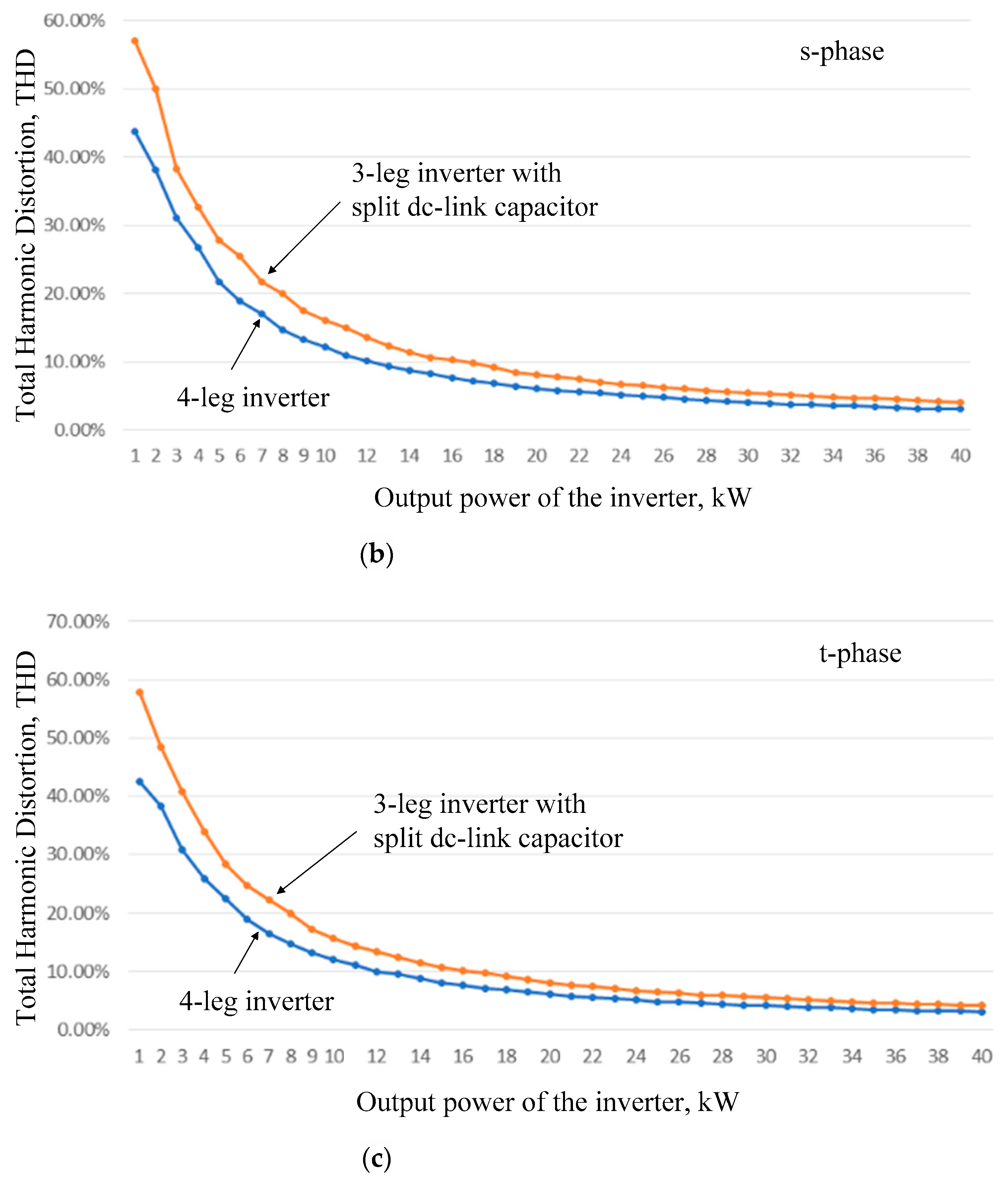
3.1.1. Comparison of THD in 3-Phase 4-Wire Inverters

First, we compared the THD according to the output power of each inverter under the balanced load condition. THD was measured from 1 kW to 40 kW. Each phase load under a balanced 3-phase condition was 10 kW (approximately 5 Ω) because it used 30 kW resistive loads at the grid voltage of 380 V. The inverter was simulated assuming that the default output power was set to 5 kW and, hence, the inverter supplied at least 5 kW of power to the grid even if the imbalance compensation algorithm was applied. The loads of the r-phase and t-phase are fixed (5 Ω each), and the magnitude of the s-phase load was reduced only, increasing the unbalance rate. In the simulation, the power output of the inverter was 10 kW, which means that the inverter supplied 10 kW to a load and the remaining 20 kW was supplied to the load from the grid. Therefore, the 30 kW condition means that the inverter was responsible for all the loads, and the 40 kW condition means that the inverter was supplying 30 kW, and the grid was supplying 10 kW.
The 3-phase 4-wire inverters showed high THD at low output power, but it tended to decrease in THD of the phase current as the output power increased. At an inverter output power of 10 kW, and the split dc-link capacitor 3-leg inverter showed a THD of 56.91%, the 4-leg inverter showed a THD of 42.42%. At 40 kW, the THD of both inverters was improved considerably: the split dc-link capacitor 3-leg inverter was 4.12% and the 4-leg inverter was 3.10%.
Figure 5 indicated the THD of the phase current depending on the load power capacity. The 4-leg inverter was superior to the split dc-link capacitor 3-leg inverter in the THD.
Figure 6 shows the THD in the phase current of the inverter as the imbalance rate of the load increases. At 3-phase 380 V and load power capacity of 30 kW (each phase load = 10 kW), it reduced the load on the s-phase, increasing the load imbalance, and the inverter was supplying default output power of 5 kW to the grid.
In both topologies, the THD of the s-phase, where the imbalance occurred, was higher than that of other phases. In the split dc-link capacitor 3-leg inverter of Figure 6a, the THD of the phase, where the imbalance occurred, did not increase, and the THD of the other two phases decreased. In the 4-leg inverter of Figure 6b, we could see that the increase in the imbalance rate in the s-phase increased the THD and decreased the THD of the other two phases.
Figure 7 is the result of the THD of the inverter output current when the inverter compensates for load imbalance due to the reduction of the s-phase load, with a constant output of 10 kW, 20 kW, and 30 kW. It could be seen that the greater the output power of the inverter, the lower the overall THD. As the s-phase load decreased and the amplitude of s-phase current decreased, the imbalance rate increased, and the THD of the s-phase increased. At the constant load conditions, the THD of the r-phase and the t-phase were reduced.
Figure 8 shows the results of the THD when increasing the s-phase load. As the load on the s-phase increased, the current on the s-phase increased, and the THD decreased. The THD on other r-phase and t-phase increased. As a result, we could confirm that the THD for inverter output current showed the same tendency when current imbalance occurred in both topologies.

3.1.2. Proposed Imbalance Compensation for Split dc-Link Capacitor 3-Leg Inverter

The above analysis showed that the 4-leg inverter had better THD characteristics than the split dc-link capacitor 3-leg inverter. However, it was much more efficient to change the preinstalled 3-leg inverter to the split dc-link capacitor 3-leg inverter structure. Therefore, in this paper, we applied the proposed offset voltage compensation algorithm for the split dc-link capacitor 3-leg inverter.
Figure 9a shows an experimental setup, and Figure 9b is a block diagram of the proposed imbalance compensation control algorithm using offset voltages. Reference generator supplies controlled the command values using active components and reactive components obtained through the d-q transformation of the load current. To obtain the amplitude and phase angle information for each phase, the current of each phase was measured, and the transformation to a synchronous coordinate frame was performed. It performed a coordinate transformation of the voltage of the inverter to generate the control commands vrn*, vsn* and vtn*. The offset voltage reference calculator used load voltage to calculate the offset voltage. Then, it transferred the obtained switching control commands (VrN*, VsN*, and VtN*) to the PWM module. The split dc-link capacitor 3-leg inverter operated as a voltage source in independent operation mode, so the voltage of the grid was always constant. However, voltage imbalance caused by single-phase loads occurred at the load terminal. The voltage imbalance rate could be reduced by subtracting it from the output voltage command of the inverter by applying the imbalance voltage generated at the neutral point as offset voltage.
V r N = V r sin ( ω t ) k ( v r N + v s N + v t N ) 3
V s N = V s sin ( ω t 2 3 π ) k ( v r N + v s N + v t N ) 3
V t N = V t sin ( ω t + 2 3 π ) k ( v r N + v s N + v t N ) 3
where k = L N L N + L f 3 ( 0 < k < 1 ) .
In (17)–(19), the output phase voltage was calculated using the sensed phase voltage whenever the controller was operated. This required no complex computation, making it easy to implement controllers, and easy to implement code on a micro control unit (MCU).
Figure 10 is a simulation result of performing an imbalance compensation using the proposed offset voltage compensation for split dc-link capacitor 3-leg inverter in independent operation mode. The load had an unbalanced current of the r-phase 71.1 A, s-phase 43.7 A, and t-phase 53.7 A. Each phase voltage was 220 V, indicating that the voltage imbalance rate was improved and that an unbalanced current was flowing to the inverter through the neutral line.
If the grid had a problem, the inverter changed from the grid-connected mode to the independent operation mode. The anti-islanding algorithm recognized the grid problems and isolated the load from the grid by turning off the switch connected to the grid. At this time, the inverter was operating as a current source in the grid-connected mode and then changed to the independent operation mode, acting as a voltage source and maintaining the magnitude of the voltage supplied to the load. Here, the inverter must maintain a constant phase angle information and frequency information, obtained using PLL, even when the mode was changed. If the output current control of the inverter was performed using the PLL information (frequency and phase angle) obtained from the grid voltage before the grid problem occurred in the inverter in independent operation mode, PLL was performed following the phase angle information obtained from the previous PLL information. At this point, the load recognized that the voltage recognized was maintaining a constant grid voltage. This means that even if it changed from the grid-connected mode to the independent operation mode, the AC voltage supplied to the load was constant (the seamless operation was possible). On the other hand, to change from the independent operation mode of the inverter to the grid-connected mode, the voltage information on the grid had to be continuously sensing, while the inverter was operating in independent operation mode. At this time, when the grid voltage and the output voltage of the inverter were synchronized, the system switched, on and the inverter changed to the grid-connected mode to act as a current source [33].
Figure 11a is the result of the proposed offset voltage control algorithm in an unbalanced load condition where the s-phase load was greater than the r-phase and t-phase load. At the load imbalance rate of 51.93%, the voltage imbalance rate was 4.98%, but it was reduced to 1.18% after applying the proposed offset voltage compensation. At the load imbalance rate of 10.44%, the voltage imbalance rate was reduced from 0.78% to 0.21%. Figure 11b shows the result of the proposed algorithm in an unbalanced load condition, where the s-phase load became smaller than the r-phase and t-phase loads. We found that at the load imbalance rate of 9.13%, the voltage imbalance rate was reduced from 0.82% to 0.20%, and at the load imbalance rate of 30.93%, the voltage imbalance rate decreased from 1.90% to 0.39%. Figure 11c shows the voltage imbalance rate in an extremely unbalanced load condition. The left graph improved the voltage imbalance rate from 5.01% to 0.90% at the load imbalance rate of 77.01% when the s-phase load is smaller than other loads. The graph on the right shows a voltage imbalance rate of 3.64% at the load imbalance rate of 92.18% when the load of s-phase is large compared to other loads.

3.2. Experiment Results

For validation of the feasibility of the imbalance voltage compensation algorithm using an offset voltage, we made the preinstalled dc-link capacitor of 6800 μF a split dc-link structure and added ac electrolytic capacitors of 50 μF up and down of the split structure. Table 2 shows the specifications of the inverter used in the experiment.
This section presented experimental results that improved the voltage imbalance through the neutral point offset voltage control when the inverter was in the independent operation mode. The Y-connected resistive loads for creating the imbalance conditions were r-phase 10 Ω, s-phase 10 Ω, and t-phase 50 Ω. For SPWM, the peak of the phase voltage was only half of the dc-link voltage (Vdc). The experiment waveform, given in Figure 12, was measured at Ma = 0.34, with Vdc of 700 V and a reference command value of the inverter of 117 V. Figure 12a shows the phase voltage of each load and neutral current in an unbalanced voltage condition. It can be seen that voltage imbalance occurred in three phases and that there was an unbalanced current flowing through the neutral line. Figure 12b shows that under voltage imbalance conditions, the phase current of each load is r-phase 8.46 A, s-phase 4.95 A, and t-phase 2.12 A. Hence, we could confirm that the imbalance occurred at each phase voltage and at each phase current because of the unbalanced load condition. Figure 12c is an experimental waveform in which the voltage in each phase was balanced by subtracting the offset voltage (Voffset) from each phase voltage command. Figure 12d shows that the amplitude of the phase current of each load changed as the voltage imbalance compensation was achieved.
The experiment waveform given in Figure 13 is measured at Ma = 0.78, with Vdc of 800 V and the reference command value of the inverter of 220 V. Figure 13a shows the phase voltage of each load and neutral current in an unbalanced voltage condition. It could be seen that voltage imbalance occurred in three phases and that there was an unbalanced current flowing through the neutral line. Figure 13b shows that under voltage imbalance conditions, the phase current of each load was the r-phase 22.3 A, s-phase 19.1 A, and t-phase 6.64 A. Consequently, we could confirm that the imbalance occurred at each phase voltage and at each phase current because of the unbalanced load condition. In this case, the unbalance rate of the output voltage was 19.15%. Figure 13c is an experimental waveform in which the voltage on each phase was balanced by subtracting the offset voltage (Voffset) from each phase voltage command. Figure 13d shows that the amplitude of the phase current of each load changed as the voltage imbalance compensation was achieved. The unbalance rate of the output voltage was reduced to 6.92%. In conclusion, we could find that the unbalance rate of the output voltage was reduced by 12.23%, compared to before, when applying the proposed compensation algorithm.
Figure 14a shows an experimental waveform when applying the proposed imbalance compensation control to a three-phase imbalance condition. Figure 14b is an enlarged waveform before voltage compensation control is applied. It could be seen that the peak of each phase voltage differed by about 20 V and that the imbalance current flowed. Figure 14c is an enlarged waveform after the proposed imbalance compensation control was applied. The phase voltage of each load was balanced, and it could be seen that the amplitude of the imbalance current changed with the voltage imbalance compensation.

4. Conclusions

Using Millman’s theorem, we analyzed the output voltage imbalance and the cause of the offset voltage in 3-phase 3-leg inverters. Based on this result, we proposed a voltage imbalance compensation algorithm using offset voltage. The circuit configuration, for which the proposed algorithm could be applied, was 3-phase 4-wire inverter structures such as split dc-link capacitor 3-leg inverter, and 4-leg inverter.
After analyzing the THD according to the imbalance rate of the load for the two inverters, it was found that the THD characteristics of the 4-leg inverter were generally good. However, in order to use a 4-leg inverter, a full replacement of the preinstalled PCS was inevitable. Therefore, we validated the validity of the proposed algorithm with PSIM simulations and experiments on a split dc-link capacitor 3-leg inverter, which could be applied by changing the circuit structure of the preinstalled 3-leg inverter.
In conclusion, we verified that the proposed output voltage compensation algorithm had the effect of improving the voltage imbalance rate by 3.64%, even under the extreme imbalance rate of the load of 92.18%.

Author Contributions

Conceptualization, S.-P.K. and S.-J.P.; data curation, S.-P.K. and F.-s.K.; formal analysis, S.-P.K. and S.-J.P.; funding acquisition, S.-G.S.; investigation, S.-P.K. and F.-s.K.; methodology, S.-G.S.; project administration, S.-G.S.; resources, S.-G.S.; software, S.-P.K.; supervision, S.-J.P. and F.-s.K.; validation, S.-P.K.; visualization, S.-J.P.; writing—original draft, S.-P.K. and F.-s.K.; writing—review & editing, F.-s.K. All authors have read and agreed to the published version of the manuscript.

Funding

This work was supported by the Korean Institute of Energy Technology Evaluation and Planning (KETEP) grant funded by the Korean government (MOTIE; 20194310100030, Development of Demonstration Zone for New Electricity Service Model).

Conflicts of Interest

The authors declare no conflict of interest.

References

  1. Kim, S.Y.; Song, S.G.; Park, S.J. Minimum Loss Discontinuous Pulse-Width Modulation Per Phase Method for Three-Phase Four-Leg Inverter. IEEE Access 2020, 8, 122923–122935. [Google Scholar] [CrossRef]
  2. Chee, S.J.; Kim, H.S.; Sul, S.K.; Ko, S. Common-Mode Voltage Reduction of Three-Level Four-Leg PWM Converter. IEEE Trans. Ind. Appl. 2015, 51, 4006–4016. [Google Scholar] [CrossRef]
  3. Dai, N.-Y.; Wong, M.-C.; Ng, F.; Han, Y.-D. A FPGA-Based Generalized Pulse Width Modulator for Three-Leg Center-Split and Four-Leg Voltage Source Inverters. IEEE Trans. Power Electron. 2008, 23, 1472–1484. [Google Scholar] [CrossRef]
  4. Kim, J.H.; Sul, S.K. A carrier-based PWM method for three-phase four-leg voltage source converters. IEEE Trans. Power Electron. 2004, 19, 66–75. [Google Scholar] [CrossRef]
  5. Kim, J.H.; Sul, S.K.; Kim, H.; Ji, J.K. A PWM strategy for four-leg voltage source converters and applications to a novel line interactive UPS in a three phase four wire system. In Proceedings of the 39th IEEE Industry Applications Conference, IAS 2004, Seattle, WA, USA, 3–7 October 2004; pp. 2202–2209. [Google Scholar]
  6. Videt, A.; Moigne, P.L.; Idir, N.; Baudesson, P.; Cimetière, X. A New Carrier-Based PWM Providing Common-Mode-Current Reduction and DC-Bus Balancing for Three-Level Inverters. IEEE Trans. Ind. Electron. 2007, 54, 3001–3011. [Google Scholar] [CrossRef]
  7. Li, F.; He, F.; Ye, Z.; Fernando, T.; Wang, X.; Zhang, X. A Simplified PWM Strategy for Three-Level Converters on Three-Phase Four-Wire Active Power Filter. IEEE Trans. Power Electron. 2018, 33, 4396–4406. [Google Scholar] [CrossRef]
  8. Tan, L.; Wu, B.; Narimani, M.; Xu, D.; Joos, G. Multicarrier-Based PWM Strategies With Complete Voltage Balance Control for NPC Inverters. IEEE Trans. Ind. Electron. 2018, 65, 2863–2872. [Google Scholar] [CrossRef]
  9. Zhang, R.; Prasad, V.H.; Boroyevich, D.; Lee, F.C. Three-dimensional space vector modulation for four leg voltage source converters. IEEE Trans. Power Electron. 2002, 17, 314–326. [Google Scholar] [CrossRef]
  10. Aissani, M.; Aliouane, K. Three-dimensional space vector modulation for four-leg voltage-source converter used as an active compensator. In Proceedings of the International Symposium on Power Electronics, Electrical Drives, Automation and Motion, SPEEDAM 2010, Pisa, Italy, 14–16 June 2010; pp. 1416–1421. [Google Scholar]
  11. Golwala, H.; Chudamani, R. New Three-Dimensional Space Vector-Based Switching Signal Generation Technique Without Null Vectors and With Reduced Switching Losses for a Grid-Connected Four-Leg Inverter. IEEE Trans. Power Electron. 2016, 31, 1026–1035. [Google Scholar] [CrossRef]
  12. Zhang, Q.; Zhang, P.; Zhao, S.; Gao, J.; Sun, X. Research on a discontinuous three-dimensional space vector modulation strategy for the three-phase four-leg inverter. In Proceedings of the IEEE 8th International Power Electronics and Motion Control Conference, IPEMC-ECCE Asia 2016, Hefei, China, 22–26 May 2016; pp. 575–580. [Google Scholar]
  13. Llonch-Masachs, M.; Heredero-Peris, D.; Montesinos-Miracle, D.; Rull-Duran, J. Understanding the three and four-leg inverter Space Vector. In Proceedings of the 18th European Conference on Power Electronics and Applications, EPE ECCE Europe 2016, Karlsruhe, Germany, 5–9 September 2016; pp. 1–10. [Google Scholar]
  14. Rojas, F.; Kennel, R.; Cardenas, R.; Repenning, R.; Clare, J.C.; Diaz, M. A New Space-Vector-Modulation Algorithm for a Three-Level Four-Leg NPC Inverter. IEEE Trans. Energy Convers. 2017, 32, 23–32. [Google Scholar] [CrossRef]
  15. Lin, F.; Tan, K.; Lai, Y.; Luo, W. Intelligent PV Power System with Unbalanced Current Compensation Using CFNN-AMF. IEEE Trans. Power Electron. 2019, 34, 8588–8598. [Google Scholar] [CrossRef]
  16. Hadidian Moghaddam, M.J.; Kalam, A.; Miveh, M.R.; Naderipour, A.; Gandoman, F.H.; Ghadimi, A.A.; Abdul-Malek, Z. Improved Voltage Unbalance and Harmonics Compensation Control Strategy for an Isolated Microgrid. Energies 2018, 11, 2688. [Google Scholar] [CrossRef] [Green Version]
  17. Jung, K.; Suh, Y. Analysis and Control of Neutral-Point Deviation in Three-Level NPC Converter Under Unbalanced Three-Phase AC Grid. IEEE Trans. Ind. Appl. 2019, 55, 4944–4955. [Google Scholar] [CrossRef]
  18. Douglass, P.J.; Trintis, I.; Munk-Nielsen, S. Voltage unbalance compensation with smart three-phase loads. In Proceedings of the Power Systems Computation Conference, PSCC 2016, Genoa, Italy, 20–24 June 2016; pp. 1–7. [Google Scholar]
  19. Hu, J.; Fu, X.; Liao, T.; Chen, X.; Ji, K.; Sheng, H.; Zhao, W. Low Voltage Distribution Network Line Loss Calculation Based on The Theory of Three-phase Unbalanced Load. In Proceedings of the 3rd International Conference on Intelligent Energy and Power Systems, IEPS 2017, Hangzhou, China, 10 October 2017; pp. 65–71. [Google Scholar]
  20. Han, J.; Oh, Y.S.; Gwon, G.H.; Kim, D.U.; Noh, C.H.; Jung, T.H.; Lee, S.J.; Kim, C.H. Modeling and Analysis of a Low-Voltage DC Distribution System. Resources 2015, 4, 713–735. [Google Scholar] [CrossRef] [Green Version]
  21. Wang, J.; Konikkara, D.D.; Monti, A. A generalized approach for harmonics and unbalanced current compensation through inverter interfaced distributed generator. In Proceedings of the IEEE 5th International Symposium on Power Electronics for Distributed Generation Systems, PEDG 2014, Galway, Ireland, 24–27 June 2014; pp. 1–8. [Google Scholar]
  22. Weidong, J.; Zhang, X.; Wang, W.; Wang, J.; Zhai, F.; Li, J.; Li, L. A Novel Modulation Strategy With Unconditional Neutral Point Voltage Balance and Three Switching Actions in One Switching Cycle for Neutral Point Clamped Three-Level Converter. IEEE Trans. Ind. Electron. 2019, 66, 5025–5038. [Google Scholar] [CrossRef]
  23. Choi, W.-H.; Lam, C.-S.; Wong, M.-C.; Han, Y.-D. Analysis of DC-Link Voltage Controls in Three-Phase Four-Wire Hybrid Active Power Filters. IEEE Trans. Power Electron. 2013, 28, 2180–2191. [Google Scholar] [CrossRef]
  24. Dong, G.; Ojo, O. Current Regulation in Four-Leg Voltage-Source Converters. IEEE Trans. Ind. Electron. 2007, 54, 2095–2105. [Google Scholar] [CrossRef]
  25. Liu, Z.; Liu, J.; Li, J. Modeling, Analysis, and Mitigation of Load Neutral Point Voltage for Three-Phase Four-Leg Inverter. IEEE Trans. Ind. Electron. 2013, 60, 2010–2021. [Google Scholar] [CrossRef]
  26. Wang, W.; Zhang, B.; Xie, F. A Novel SVPWM for Three-Level NPC Inverter Based on m-Mode Controllability. IEEE Trans. Ind. Electron. 2018, 65, 6055–6065. [Google Scholar] [CrossRef]
  27. Bifaretti, S.; Lidozzi, A.; Solero, L.; Crescimbini, F. Comparison of modulation techniques for active split dc-bus three-phase four-leg inverters. In Proceedings of the IEEE Energy Conversion Congress and Exposition, ECCE 2014, Pittsburgh, PA, USA, 14–18 September 2014; pp. 14–18. [Google Scholar]
  28. Kwak, Y.-g.; Heo, D.-h.; Kim, S.-p.; Song, S.-G.; Park, S.-J.; Kang, F.-s. Reliability and Economic Efficiency Analysis of 4-leg Inverter Compared with 3-leg Inverters. Electronics 2021, 10, 87. [Google Scholar] [CrossRef]
  29. Lin, Z.; Ruan, X.; Jia, L.; Zhao, W.; Liu, H.; Rao, P. Optimized Design of the Neutral Inductor and Filter Inductors in Three-Phase Four-Wire Inverter with Split DC-Link Capacitors. IEEE Trans. Power Electron. 2019, 34, 247–262. [Google Scholar] [CrossRef]
  30. Dai, M.; Marwali, M.N.; Jung, J.W.; Keyhani, A. A Three-Phase Four-Wire Inverter Control Technique for a Single Distributed Generation Unit in Island Mode. IEEE Trans. Power Electron. 2008, 23, 322–331. [Google Scholar] [CrossRef]
  31. Bozalakov, D.; Meersman, B.; Bottenberg, A.L.; Rens, J.; Desmet, J.; Vandevelde, L. Dc-bus voltage balancing controllers for split dc-link four-wire inverters and their impact on the quality of the injected currents. In Proceedings of the 24th Inter-national Conference and Exhibition on ELECTRICITY DISTRIBUTION Glasgow, CIRED 2017, Glasgow, UK, 12–15 June 2017; pp. 564–568. [Google Scholar]
  32. Kjaer, S.; Pedersen, J.; Blaabjerg, F. A review of single-phase grid-connected inverters for photovoltaic modules. IEEE Trans. Ind. Appl. 2005, 41, 1292–1306. [Google Scholar] [CrossRef]
  33. Kim, S.-P.; Song, S.-G.; Park, S.-J.; Kang, F.-S. Imbalance Compensation Algorithm using Effective and Reactive Power for Split DC-link Capacitor 3-Leg Inverter. IEEE Access 2021. under review. [Google Scholar]
Figure 1. Circuit configuration of a 3-phase 3-leg inverter.
Electronics 10 01029 g001
Figure 2. Offset voltage of a 3-leg inverter by the theorem of superposition: (a) dc component of the offset voltage; (b) ac component of the offset voltage.
Electronics 10 01029 g002
Figure 3. Control block diagram of an unbalanced 3-phase voltage compensation: (a) prior approach using independent control for each phase; (b) proposed approach using offset voltage of the neutral point of the load.
Electronics 10 01029 g003
Figure 4. Circuit configuration of a 3-phase 4-wire inverters: (a) 3-leg inverter employing split-dc-link capacitor; (b) 4-leg inverter.
Electronics 10 01029 g004
Figure 5. Comparison of total harmonic distortion (THD) of the phase current with the increase in the output power of the 3-phase 4-wire inverters: (a) r-phase; (b) s-phase; (c) t-phase.
Electronics 10 01029 g005aElectronics 10 01029 g005b
Figure 6. Comparison of THD of the phase current according to the increase in the unbalance rate in s-phase: (a) 3-leg inverter employing split dc-link capacitor; (b) 4-leg inverter.
Electronics 10 01029 g006
Figure 7. Comparison of the THD of the inverter output current when the inverter compensates for load imbalance due to the reduction of the s-phase load, with a constant output: (a) split dc-link capacitor 3-leg inverter; (b) 4-leg inverter.
Electronics 10 01029 g007
Figure 8. Comparison of THD of the inverter output current when the inverter compensates for load imbalance due to the increase in the s-phase load with a constant output: (a) split dc-link capacitor 3-leg inverter; (b) 4-leg inverter.
Electronics 10 01029 g008
Figure 9. Experimental setup and control block diagram; (a) experimental setup; (b) block diagram of the proposed imbalance compensation using offset voltages.
Electronics 10 01029 g009aElectronics 10 01029 g009b
Figure 10. Simulation results of imbalance voltage compensation using the offset voltage for split dc-link capacitor 3-leg inverter in the independent operation mode.
Electronics 10 01029 g010
Figure 11. Voltage imbalance rate according to the unbalanced load conditions: (a) s-phase load is greater than r-, t-phase; (b) s-phase load is smaller than r-, t-phase; (c) under extreme unbalanced load conditions.
Electronics 10 01029 g011
Figure 12. Experimental results that improve voltage imbalance through offset voltage (Voffset) control when the inverter is in the independent operation mode, Ma = 0.34 with Vdc of 700 V and the reference command value of the inverter of 117 V: (a) phase voltage of each load and neutral line current in an unbalanced voltage condition; (b) phase current of each load under voltage imbalance conditions; (c) the voltage on each phase is balanced by subtracting the offset voltage from each phase voltage command of the inverter; (d) phase current of each load under voltage-balanced condition.
Electronics 10 01029 g012
Figure 13. Experimental results that improve voltage imbalance through offset voltage (Voffset) control when the inverter is in the independent operation mode, Ma = 0.78 with Vdc of 800 V and the reference command value of the inverter of 220 V: (a) phase voltage of each load and neutral line current in an unbalanced voltage condition; (b) phase current of each load under voltage imbalance conditions; (c) the voltage on each phase is balanced by subtracting the offset voltage from each phase voltage command of the inverter; (d) phase current of each load under voltage-balanced condition.
Electronics 10 01029 g013
Figure 14. Experimental results before and after applying the proposed imbalance compensation control: (a) when applying the proposed voltage compensation control to a three-phase imbalance condition; (b) enlarged waveform before voltage compensation control is applied; (c) enlarged waveform after the proposed voltage compensation control is applied.
Electronics 10 01029 g014
Table 1. Simulation and experiment parameters.
ItemValueUnit
dc-link voltage800V
Filter inductor1.5mH
Neutral inductor3.6mH
dc electrolytic capacitor * 6800μF
ac electrolytic capacitor *50μF
Filter capacitor40μF
Switching frequency10kHz
Load Power30kW
Power factor0.99PF
Load unbalance factor (LUF)0~30%
* split dc-link capacitor.
Table 2. Specifications of split dc-link capacitor 3-leg inverter for the experiment.
ItemValueUnit
Operating range of input voltageDC 650–830V
Maximum allowable input voltageDC 900V
Output power10kW
Output voltageAC 380V
Output current20A
Output frequency60Hz
Total harmonic distortion<2%
Publisher’s Note: MDPI stays neutral with regard to jurisdictional claims in published maps and institutional affiliations.

