Article

A Low-Complexity Edward-Curve Point Multiplication Architecture

1
Science and Technology Unit (STU), Umm Al-Qura University, Makkah 24382, Saudi Arabia
2
Department of Computer Engineering, Umm Al-Qura University, Makkah 24382, Saudi Arabia
3
Electrical Engineering Department, Bahria University, Islamabad 44000, Pakistan
*
Author to whom correspondence should be addressed.
Electronics 2021, 10(9), 1080; https://doi.org/10.3390/electronics10091080
Submission received: 21 March 2021 / Revised: 24 April 2021 / Accepted: 26 April 2021 / Published: 3 May 2021
(This article belongs to the Section Computer Science & Engineering)

Abstract

:
The Binary Edwards Curves (BEC) are becoming more and more important, as compared to other forms of elliptic curves, thanks to their faster operations and resistance against side channel attacks. This work provides a low-complexity architecture for point multiplication computations using BEC over G F ( 2 233 ) . There are three major contributions in this article. The first contribution is the reduction of instruction-level complexity for unified point addition and point doubling laws by eliminating multiple operations in a single instruction format. The second contribution is the optimization of hardware resources by minimizing the number of required storage elements. Finally, the third contribution is to reduce the number of required clock cycles by incorporating a 32- b i t finite field digit-parallel multiplier in the datapath. As a result, the achieved throughput over area ratio over G F ( 2 233 ) on Virtex-4, Virtex-5, Virtex-6 and Virtex-7 Xilinx FPGA (Field Programmable Gate Array) devices are 2.29, 19.49, 21.5 and 20.82, respectively. Furthermore, on the Virtex-7 device, the required computation time for one point multiplication operation is 18 µs, while the power consumption is 266 mW. This reveals that the proposed architecture is best suited for those applications where the optimization of both area and throughput parameters are required at the same time.

1. Introduction

The internet-of-things (IoT) concerns a global network, where billions of heterogeneous devices are required to connect with an unsecured internet [1]. The connected devices share information (or) data with each other. Since most of the devices in an IoT framework have constrained resources, data are usually stored in the cloud [2]. As a result, the users can continuously upload and download data from anywhere using the internet [3]. Due to this enormous communication of IoT devices through a cloud, they are subject to malicious attacks [4]. Security concerns arise, and therefore various threats and attacks may occur as data owners have no control over the data management [5]. Consequently, the importance of data security and the availability of limited resources provoke us to explore recent low-complexity cryptographic schemes [6].
Elliptic-curve cryptography (ECC), a public-key cryptography scheme, has become an attractive approach to target many applications like IoT security [7]. The main motivation behind the wide spread adoption of ECC is its ability to provide a similar security level with a relatively smaller key-sizes [8]. It comprises of four layers [9]. The top most layer (fourth layer) is the protocol layer which ensures the encryption and decryption of data. In layer three, the scalar (or) point multiplication (PM) is computed which is the most critical operation. For PM computation, the point addition (PA) and point doubling (PD) operations are performed in layer two. Finally, the layer one of ECC consists of finite-filed (FF) arithmetic operations (addition, multiplication, square and inversion). In addition to the layer model of ECC, there are two coordinate systems, i.e., affine and projective. The latter is more frequently employed to achieve a high throughput [10]. Furthermore, two field representations, prime ( G F ( P ) ) and binary ( G F ( 2 m ) ), are commonly available. The prime field representation is generally utilized for software based implementations while the binary field representation is preferred for hardware deployments [11].
As far as the security of ECC is concerned, it offers a variety of implementation models, such as weierstrass [12], binary-edward (BEC) [13], hessian (HC) [14] and binary-huff (BHC) [15]. The Weierstrass model is the fundamental ECC model, however, it may expose secret-key via simple power analysis (SPA) attacks [10]. The vulnerability of Weierstrass model to SPA attacks is due to different mathematical formulations of PA and PD for PM computation [9]. The SPA is a type of side channel attack. In SPA, attackers can come into a secret-key in terms of zeros and ones by inspecting the power trails of PA and PD computations. The power trails are inspected using various power analysis tools such as logic analyzer [16]. Among several other choices, one of the solution to resist SPA attacks in ECC is the use of unified PA and PD laws.
Except the weierstrass model of ECC, all the aforementioned models (HC, BEC, BHC) provide unified mathematical formulations for the computation of PA and PD operations [13,14,15]. As compared to BEC and HC, the BHC model of ECC has a relatively higher mathematical complexity in unified PA and PD laws. The higher mathematical complexity requires more hardware resources and ultimately consumes more power [15]. Therefore, the use of BHC model in IoT related applications is less attractive. On the other hand, the BEC model is usually preferred to achieve a higher throughput while utilizing lower hardware resources as compared to HC model of ECC [17]. For complete mathematical structures of various unified PA and PD laws of ECC models, the interested readers are referred to [18]. The objective of this article is to propose a low-complexity point multiplication design on an FPGA (Field Programmable Gate Array) platform for BEC model of ECC. In the following, state-of-the-art BEC implementations on FPGA and their limitations are provided.

1.1. Related Work for BEC Implementations

The work in [19] presents a re-configurable processor architecture, using point halving and unified point doubling approaches, for the computation of PM operation. When considering only the point halving method, the authors in [19] utilize 22,373 Slices. For the point doubling case, the utilized slices are 21,816. For both these techniques (point halving and unified point doubling), the maximum operational clock frequency is 48 MHz on Virtex-4 device. Similarly, for different BEC coefficients (represented as d), two different architectures are described in [20]. In the first architecture, a single Gaussian basis FF multiplier is used while the second architecture advocates the use of three parallel FF Gaussian basis multipliers. The larger design with three FF multipliers utilizes higher hardware resources (29,255 Slices—when the value for d = 59 ) on Virtex-4 device as compared to the architecture with one FF multiplier (12,403 Slices—when the value for d = 59 ). For different values of d (59 and 26), the architectures described in [20] achieve various clock frequencies and require different times (in s) for the PM computation process.
While the focus in [19,20] is to optimize throughput, however, the optimization of required number of clock cycles is equally important. In order to reduce the total number of clock cycles, the work in [21] employs three digit-serial multipliers. Furthermore, it employs a pipelining technique which reduces the critical path and improves clock frequency. Similar to [21], another hardware solution is reported in [22] where a pipelined digit-serial multiplier is used. This digit-serial use of multiplier results 31,702 (on Virtex-4 when d = 59 ), 4987 (on Virtex-5 when d = 26 ) and 11,494 (on Virtex-5 when d = 59 ) slices.
For area optimization, an interesting solution on Virtex-5 device is described in [23]. At first, the instruction-level-parallelism is employed to optimize the clock frequency (308 MHz), which is comparatively higher than the solution provided in [19]. Subsequently, the area (15,804 Slices) is reduced by using a single FF arithmetic operator (adder, multiplier, squarer and inverter) in the datapath of the cryptoprocessor. The most efficient area optimized architecture is implemented on Virtex-6 in [24]. Here, a bit-serial approach for FF multiplication is employed instead of a digit-serial multiplier (as used in solutions [20,21,22]). Moreover, this solution takes 6720 s for one PM computation.
For optimizing different design parameters (i.e., latency, area, power, etc.,) the most recent architectures are reported in [25,26,27,28,29]. In [25], a comb PM algorithm is utilized to achieve low-complexity (LC) and low-latency (LL) architectures. The LC architecture provides 62%, 46% and 152% improvements over G F ( 2 233 ) , G F ( 2 163 ) and G F ( 2 283 ) , respectively. On the other hand, the LL architecture reduces the time required to compute one PM operation. An interesting solution is described in [26] where a new modular reduction method is provided. Rather than applying a full modular reduction, the modular reduction approach of [26] iteratively performs reductions on partial products. As a result, the latency of modular multiplication operation is reduced. The complete ECC architecture is synthesized for 180-nm common-metal-oxide-semiconductor (CMOS) process technology over G F ( p ) with p = 256 bits. It utilizes 144.8–65.4 k logic gates (or gate counts).
In [27], a low-cost as well as fast hardware implementations for BEC are reported. The low-cost implementation is achieved by incorporating one pipelined digit-serial modular multiplier. On the other hand, three parallel multipliers are used to accelerate PA and PD computations. Similarly, a low-power and low-area implementation is described in [28] where a high-radix interleaved modular multiplication method is utilized. Recently, a high-speed, low-area and SPA-resistant processor architecture is described in [29]. The processor architecture performs 256- b i t PM in 198,715 clock cycles and requires 1.9 ms (for Virtex-7) and 2.13 ms (for Virtex-6). The architecture utilizes only 6543 slices on Virtex-7 FPGA.

1.2. Limitations of Existing Practices

Section 1.1 reveals that various FF multipliers can be employed in the datapath of PM architectures, either to optimize area or throughput. The use of a bit-serial FF multiplier decreases area (hardware resources) while decreasing the overall throughput of BEC architecture/design [24]. On the other hand, the use of a digit-serial FF multiplier, as employed in [20,21,22], increases throughput with the expanse of higher hardware resources. However, there are various area constrained applications such as RFID cards [30] and digital management systems [31], which require a trade-off between throughput, area and power consumption.

1.3. Contributions

The contributions of this work are given as:
  • A low-complexity binary edward-curve PM architecture over G F ( 2 m ) with m = 233 is proposed.
  • For unified PA and PD laws of BEC, the instruction-level-complexity is reduced by eliminating multiple operations in a single instruction format (details are provided in Section 3.2.1).
  • To save hardware resources and reduce clock cycles, the minimization of storage elements is provided by using efficient replacements of required memory addresses. It shows 7.2% decrease in total number of required clock cycles and 28.5% decrease in hardware resources (see Section 3.2.2).
  • A 32- b i t digit-parallel FF multiplier is employed instead of bit-serial and digit-serial FF multipliers. For one FF multiplication, the digit-parallel requires only one clock cycle while the bit-serial and digit-serial FF multipliers require m and m v clock cycles (where, m is the field size and v is the digit-size). The used FF multiplier ultimately reduces the required number of clock cycles.
  • To speed-up control functionalities, a Finite State Machine (FSM) controller is used in this work.
The implementation results after synthesis over G F ( 2 233 ) on Virtex-7 FPGA device reveal that the proposed low-complexity architecture takes 3244 clock cycles. Moreover, for different values of d, i.e., 59 and 26, it achieves an operational clock frequency of 179 MHz and utilizes only 2662 slices. The time required for the computation of one PM operation is 18s while the power consumption of the architecture is 266 mW. It has been observed that the proposed architecture in this article provides higher throughput over slice figures with respect to the most recent state-of-the-art solutions, described in [19,20,21,22,23,24,27].
As compared to state-of-the-art power-efficient architectures, reported in [28,29], the proposed architecture is much faster while consuming relatively more power. The power consumption increase due to the use of digit-parallel multiplier. The digit-serial multiplier approach, as employed in [28], is more convenient to reduce area and power parameters while compromising on the throughput. On the other hand, the digit-parallel and the bit-parallel multiplication methods are useful to optimize the overall performance (throughput) of the architecture.
The remainder of this paper is structured as follows: In Section 2, the mathematical background pertaining to the computation of PM on BEC model of ECC over G F ( 2 m ) is presented. The optimization of unified PA and PD operations for BEC is described in Section 3. The proposed low-complexity architecture for the PM computation of BEC is described in Section 4. Subsequently, Section 5 presents implementation results and provides a comparison in terms of various performance attributes. Finally, Section 6 concludes the paper.

2. Mathematical Background

This section provides a brief mathematical background on BEC over G F ( 2 m ) in Section 2.1. Subsequently, the unified PA and PD laws of BEC over G F ( 2 m ) and Montgomery Ladder algorithm for point multiplication are described in Section 2.2 and Section 2.3, respectively.

2.1. BEC over G F ( 2 m )

The Weierstrass equations are generally used to represent different forms of Elliptic curves such as BEC, BHC and Hessian curves [12]. The BEC curves for PM computation process, using some definite group law operations, are initially introduced in [13]. If d 1 and d 2 are the elements of G F ( 2 m ) such that d 1 0 and d 2 d 1 ( d 1 + 1 ) , then the BEC with co-coefficients d 1 and d 2 can be expressed mathematically as:
E B , d 1 , d 2 : d 1 ( x + y ) + d 2 ( x + y ) 2 = x y ( x + 1 ) ( y + 1 )
In Equation (1), x and y are the coordinates of the initial point P while d 1 and d 2 are the curve constants/parameters.

2.2. Differential PA and PD Laws for BEC over G F ( 2 m )

The differential PA and PD formulations over G F ( 2 m ) for BEC [21] are shown in Table 1. The first column of Table 1 shows the total number of required instructions ( I n s t i ) for PA and PD while the second column represents the corresponding instructions. It can be observed from Table 1 that there are 7 instructions in total with the requirement of 11 storage elements. The values e 1 , e 2 and e are given as: e 1 = e 4 , e 2 = e and e = d 1 4 + d 1 3 + d 1 2 d 2 . In order to understand the mathematical formulation comprehensively, the interested readers are referred to [32]. As shown in Table 1, W 1 , Z 1 , W 2 and Z 2 are the initial projective points, whereas Z a , Z d , W a and W d are the final projective points in BEC model. Moreover, A, B and C are the storage elements, which are required to hold the intermediate results. Similarly, w is the rational function for an elliptic curve E over G F ( 2 m ) . It is presented by a fraction of polynomials in the coordinate ring of E over G F ( 2 m ) and can be calculated as: w ( P ) = x + y d 1 ( x + y + 1 for P = ( x , y ) in E B , d 1 , d 2 . The w c o o r d i n a t e differential addition and doubling implies to calculate w ( 2 P 1 ) and w ( P 1 + P 2 ) from the given values w ( P 1 ) , w ( P 2 ) and w ( P 1 P 2 ) , where P 1 and P 2 are the points on E over G F ( 2 m ) .

2.3. Point Multiplication on BEC

Point multiplication is the result of addition of K copies at initial point P, i.e., Q = k . p = K ( P + P + , , + P ) . The term Q determines the resultant point on the defined BEC curve, K is a scalar multiplier while P is the initial point on the selected/defined BEC curve. Therefore, the following Montgomery point multiplication algorithm, known as Montgomery ladder algorithm, (shown as Algorithm 1 in the following), is employed.
Algorithm 1: Montgomery point multiplication algorithm [20]
Electronics 10 01080 i001
It can be observed from Algorithm 1 that the point multiplication is the process of computing k P for a given point P on the elliptic curve E defined over a finite field G F ( 2 m ) and a given integer k. The algorithm starts with the initialization phase. It is important to note that one addition and one doubling is performed in each step of Algorithm 1, which makes this method invulnerable against side-channel invasions [21]. In general, the primary computation for each step of the Montgomery ladder is differential doubling and addition law (dADD), as shown in Algorithm 1. In the second step of Algorithm 1, the value k i is used, where k i is the i t h bit of the scalar number k. Based on the value of k i , loop iterations are computed. If k i = 1 , the values W 2 and Z 2 are set as the inputs of the doubling computation. Otherwise, W 1 and Z 1 are selected.

3. Optimization of Differential Addition Law for BEC

The complete differential equations for PA and PD operations, shown in Table 1, require higher hardware resources for the PM computation process [21]. Therefore, this section provides an optimized version of differential addition law from the utilization of hardware resources point of view. First, Section 3.1 identifies the limitations in standard PA and PD laws for BEC. Subsequently, the optimizations are presented in Section 3.2 to address the identified limitations.

3.1. Limitations of the PA Law for BEC

The limitations of complete PA and PD operations, shown in Table 1, are listed below:
  • There are total 7 complex mathematical instructions, which are required for the complete PA and PD law (i.e., I n s t r 1 to I n s t r 7 ), as shown in column 2 of Table 1. The term complexity implies that there are many arithmetic operations in a single instruction. These operations are performed in parallel, which results in higher hardware resources.
  • The total number of storage elements, required for the complete PA and PD law of Table 1, are 11 × m . The number 11 indicates the total storage elements while m determines the width of each element. The requirement of high storage elements ultimately increases the hardware resources utilization.
To optimize the utilization of hardware resources, it is necessary to tackle the aforementioned limitations.

3.2. Proposed Optimizations

The improvements in the instructions of Table 1 are listed as: (1) Elimination of multiple operations in a single instruction and (2) minimization of storage elements.

3.2.1. Elimination of Multiple Operations in a Single Instruction

By eliminating multiple operations in a single instruction, the complexity of instructions can be reduced, as shown in Table 2. The first and second columns of Table 2 provide the required number of clock cycles and instructions for the execution of differential addition law. Consequently, the single-operator-form of differential addition law for BEC is shown in column 3. The single-operator-form of column 3 has reduced the complexity of instructions by eliminating multiple operations. However, it can be observed that the number of instructions have increased from 7 (shown in Table 1) to 14 (shown in Table 2). Additionally, it also shows an increase in the required number of storage elements from 11 (shown in Table 1) to 14 (see column 3 in Table 2) for implementing Algorithm 1.

3.2.2. Minimization of Storage Elements

The mathematical formulations, shown in column 3 of Table 2, require a total of 14 memory elements (i.e., A, B, C, W d , Z d , W a , Z a , W 1 , W 2 , Z 1 , Z 2 , T 1 to T 3 ). The memory elements W 1 , Z 1 , W 2 and Z 2 are utilized to keep the values of initial projective points while W a , Z a , W d and Z d (shown with red color in column 3 of Table 2) are employed to hold the updated values of the final projective point. The remaining elements A, B, C and T 1 to T 4 are used to store intermediate results. In order to reduce the overall memory requirements, the number of storage elements in column 3 can be reduced, as shown in column 4 of Table 2. The required memory size, for the optimized formulations in column 4, is 10 × m . The storage elements W 1 , W 2 , Z 1 and Z 2 are utilized to keep the values of initial projective points. Moreover, the storage elements W 0 , T 1 , T 3 and T 4 (shown with blue color in column 4) are used to hold the updated values of the final projective point. The remaining storage elements ( Z 0 and T 2 ) are employed to store intermediate results.
As shown in columns 3 and 4 of Table 2, the operations performed in i n s t 1 to i n s t 6 and i n s t 9 to i n s t 14 are identical. However, i n s t 7 ( T 3 = T 2 × T 2 ) and i n s t 8 ( Z d = T 3 × T 3 ) in column 3 of Table 2 can be performed in one clock cycle, as they involve frequent multiplications to be performed. In order to operate two multiplications in one clock cycle, an immediate squaring after multiplication operation can be computed, as given in i n s t 8 of column 4. It results a decrease in the total number of instructions from 14 to 13 (see columns 3 and 4 of Table 2). Moreover, there is a decrease in the number of storage elements from 14 × m to 10 × m . Furthermore, it also allows to reduce m clock cycles when m bit key length is targeted for the PM computation of BEC (see Step-2 of Algorithm 1). To summarize, the proposed optimized formulations (given in column 4 of Table 2) result in 7.2% (ratio of 13 to 14) decrease in total number of required clock cycles. Furthermore, a reduction of 28.5% (ratio of 10 to 14) in hardware resources is obtained.

4. Proposed Binary Edward Curve Point Multiplication Architecture

The proposed area-optimized PM architecture for BEC comprises of three major modules: Memory unit (MU), Data path unit (DU) and Control Unit (CU). Figure 1 and Figure 2 provide the simplified and detailed representations of the architecture, respectively. The initial curve parameters are selected from the recommended document of National Institute of Standards and Technology (NIST) [33] over G F ( 2 233 ) for binary curves. The description of aforementioned modules (MU, DP and CU) are presented in Section 4.1, Section 4.2 and Section 4.3, respectively.

4.1. Memory Unit

The memory unit consists of a Register File with a size of 10 × m , where 10 is the total number of cells/locations and m determines the size of a particular cell. The objective of Register File is to keep the initial and the final projective points using 8 MU locations for storing W 1 , Z 1 , W 2 , Z 2 , W 0 , T 1 , T 3 , T 4 . The remaining 2 locations are used to keep the intermediate results ( Z 0 , T 2 ). Similarly, the two 10 × 1 muxes are used to read the data from Register File, using the corresponding control signals (C1 and C2). The output of these multiplexers are operand 1 ( O P 1 ) and operand 2 ( O P 2 ). Furthermore, a 1 × 10 de-multiplexer is used to update the Register File through a control signal C3.

4.2. Data Path Unit

The data path unit consists of an Arithmetic Logic Unit (ALU) and three routing networks ( M U X 1 , M U X 2 and M U X 3 ).

4.2.1. Routing Networks

The size of M U X 1 and M U X 2 is 6 × 1 while the size of MUX3 is 3 × 1 . The inputs to M U X 1 and M U X 2 are initial curve parameters ( e 1 , e 2 , w ) , basepoint (x,y) and the operands from MU ( O P 1 and O P 2 ). The outputs of M U X 1 and M U X 2 are O P _ 1 and O P _ 2 , respectively, while the corresponding control signals for these two muxes are C4 and C5, respectively. The outputs O P _ 1 and O P _ 2 enter into ALU for further processing. Finally, the inputs to M U X 3 can be either from adder ( A _ o u t ), multiplier ( M _ o u t ) or squarer ( M S _ o u t ). Consequently, using the control signal C6, the output from M U X 3 is written into Register File through a 1 × 10 de-multiplexer.

4.2.2. Arithmetic Logic Unit

The arithmetic logic unit comprises of an adder, a multiplier and a squarer unit. As shown in Figure 2, the adder and the multiplier units are connected in parallel. However, the squarer unit is connected serially after the multiplier. The adder unit performs the polynomial addition using the bitwise exclusive-OR (XOR) gate. To perform multiplication over 232- b i t polynomials, a digit parallel multiplier is incorporated inside the ALU, as shown in Figure 3. The multiplier architecture consists of four-blocks: (1) Splitter, (2) multiplication, (3) concatenation and (4) reduction.
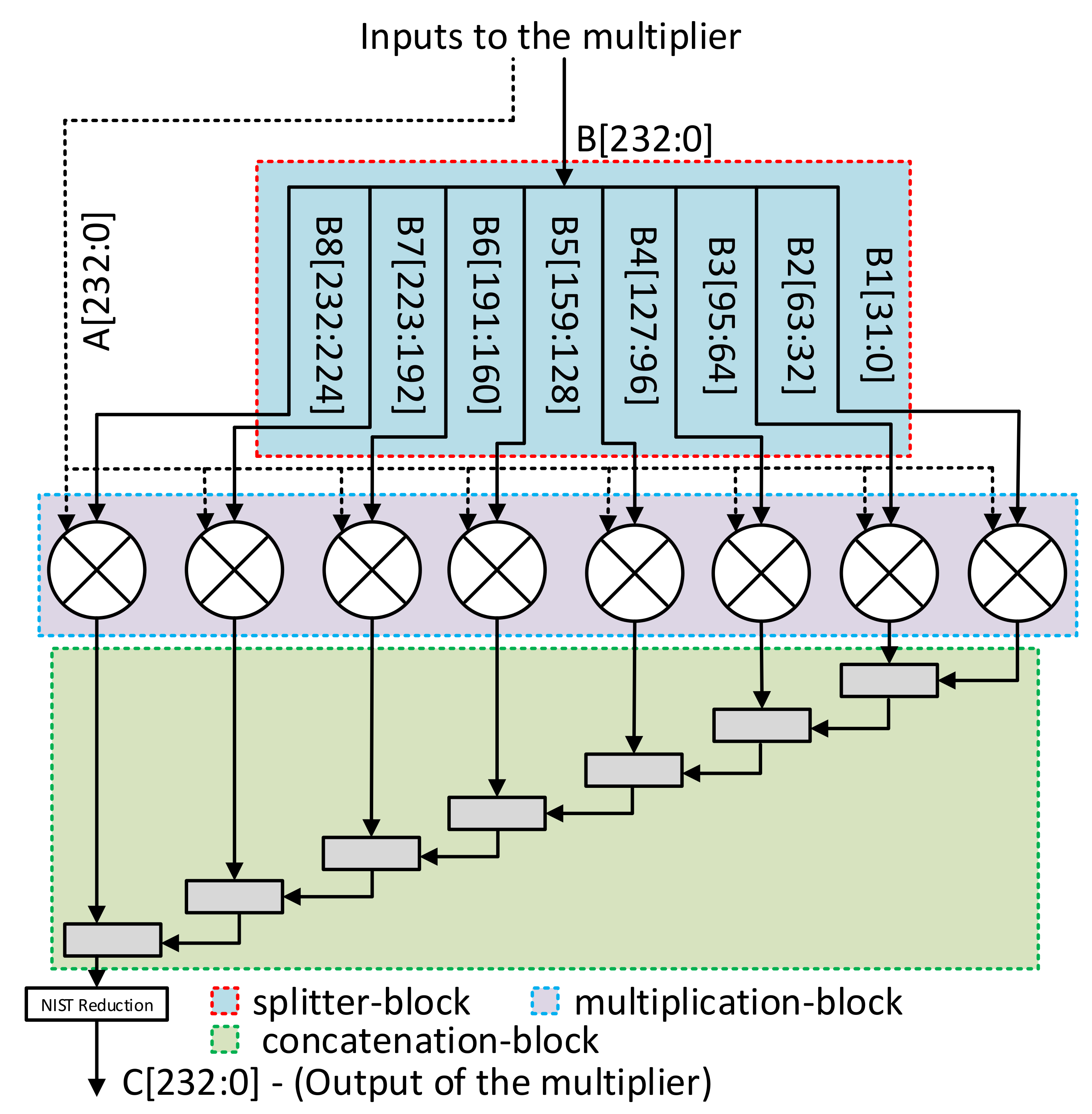
  • splitter-block: The splitter-block takes one 233- b i t polynomial (i.e., B) as an input and results digits (i.e., B 1 to B 8 ) of polynomial B as an output. In other words, it is responsible to split one input polynomial out of the required two (the multiplier requires two operands as inputs and results one operand as an output). The selection of an operand to split always depends on the designer. Figure 3 shows that the input polynomial is divided B into eight digits, i.e., B 1 to B 8 , with a digit size of 32- b i t s each except the last digit, i.e., B 8 . To perform multiplication, the required size for the last digit is 9- b i t s .
  • multiplication-block: As shown in Figure 3, the complete multiplication-block comprises of eight instances of smaller multipliers. Each smaller instance of a multiplier is responsible to perform a polynomial multiplication in parallel. Furthermore, it takes two input polynomials. These polynomials are A and a digit of polynomial B. The corresponding lengths of A and B are 232 and 32- b i t s , respectively. Consequently, the output of each instance of a smaller multiplier is d + m 1 - b i t s . Here, d represents the size of each created digit of polynomial B (i.e., 32- b i t s ). Similarly, m shows the length of input polynomial A (i.e., 233- b i t s ).
  • concatenation-block: The concatenation-block takes eight inputs. The length of each input is d + m 1 - b i t s each (generated by the multiplication-block). It provides an output polynomial of length 2 × m 1 - b i t s . The length of output polynomial is not shown in Figure 3. The internal structure of a concatenation block consists of seven arrays of XOR gates. These arrays are shown with the gray color blocks inside the concatenation-block of Figure 3. The concatenation operation is performed using shift and add operations.
  • reduction-block: To produce a resultant polynomial of m- b i t s , a finite field reduction operation over polynomial of length 2 × m 1 - b i t s is performed [11]. Therefore, a NIST recommended polynomial reduction algorithm is utilized in this work as employed in [11] over G F ( 2 233 ) .
The square module is implemented by the placement of 0 after each input data bit, as implemented for Weierstrass model in [11]. Similar to the multiplication operation, a reduction over polynomial of length 2 × m 1 - b i t s is computed. As a result, an instance of a reduction-block is utilized inside the squarer module. It results an m- b i t polynomial after squarer. The inversion operation is performed by using the multiplier and the squarer modules. Furthermore, the Quad block version of Itoh-Tsujii algorithm [34] is used for the inversion operation. The Quad block version provides better results in terms of clock cycles as compared to the square version [11].

4.3. Control Unit

To generate control signals, an FSM based dedicated control unit is used in this work, as given in Figure 4. The CU incorporates a total of 63 states. The description about these states are provided in the text as follows:
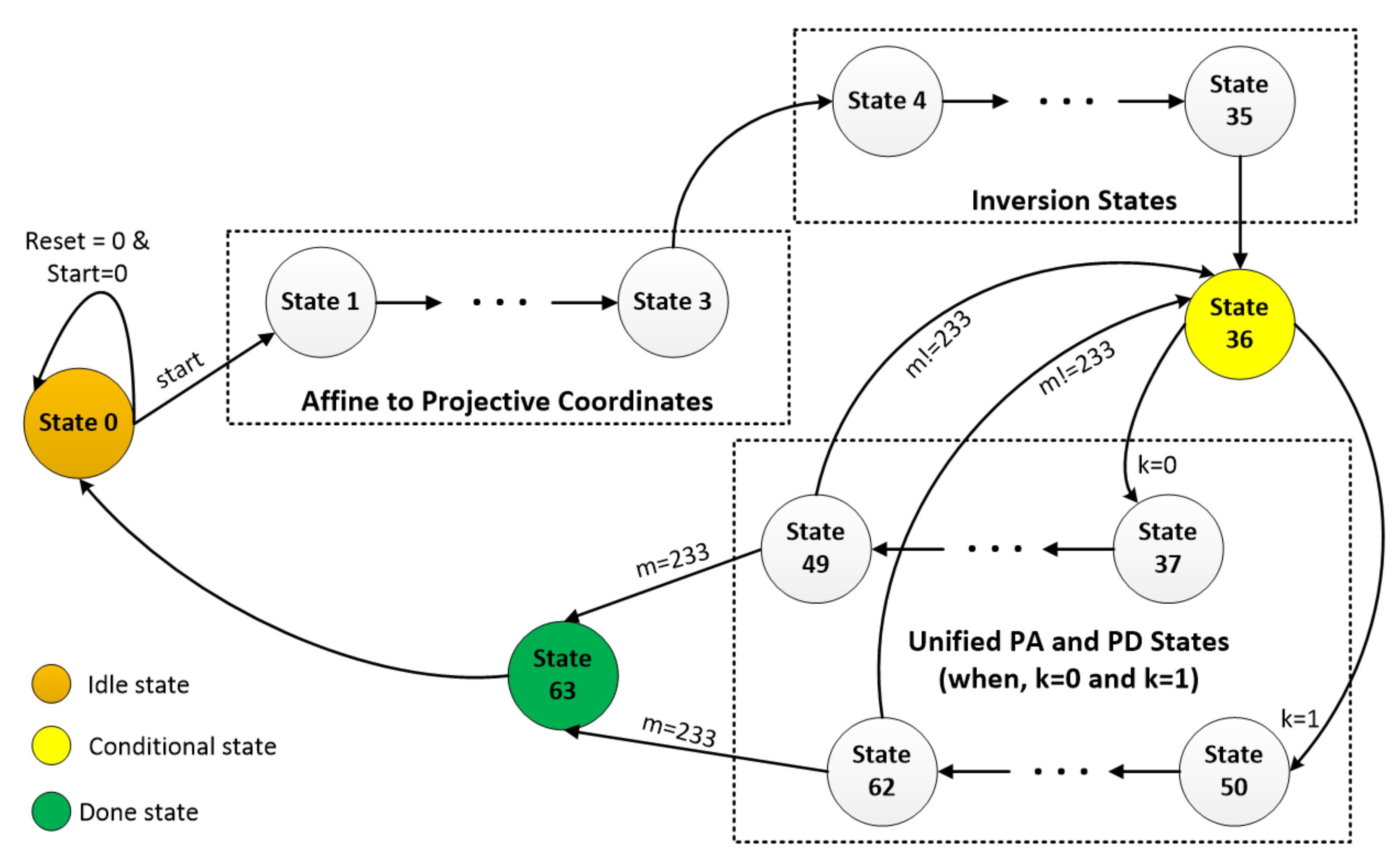
  • State 0 is an idle state. The reset and start signals determine the start of execution process.
  • Once the start signal becomes 1, the current state (State 0) of the processor switches to nextstate (State 1), as shown in Figure 2. Moreover, the State 1 to State 3 generate control signals for the affine to projective conversions of Algorithm 1.
  • The State 4 to State 35 generate control signals for inversion operation using Quad block Ithoh-Tusuji algorithm of [34].
  • State 36 counts the number of points on the specified BEC curve. Additionally, it also checks the inspected key bit (k). If the value of k is 1, the nextstate from State 36 is 50, otherwise the nextstate is State 37, as shown in Figure 4.
  • State 50 to State 62 compute i f part of the Algorithm 1. Similarly, State 37 to State 49 generate control signals for the e l s e part of Algorithm 1. For each value of k (either 0 or 1), the last states, i.e., State 49 and State 62, also check the number of points (using m in Figure 4) on the specified BEC curve. Once the value for m becomes 233 (initially, it is set to 1), the next state from State 49 and State 62 becomes State 63, otherwise the nextstate is State 36. Finally, the last state (State 63) sets the d o n e signal indicating that processor has finished the computation of PM operation and returns back to State 0.
In the proposed low-complexity architecture, Equation (2) is used to compute the total number of clock cycles (CCs). The term I n i t i a l refers to the initialisation part of Algorithm 1, whereas m determines the key length. Furthermore I n v defines the inversion operation as described in Equation (2). The first column of Table 3 provides the key length. The second column determines the required CCs for the initialisation part (initial) of Algorithm 1, whereas the total CCs for the computations of PA and PD in Algorithm 1 are presented in column three. The fourth column provides the required CCs for inversion (Inv) part of Algorithm 1. Finally, the last column of Table 3 shows the total CCs for implementing Algorithm 1.
C l o c k c y c l e s = I n i t i a l + 13 ( m 1 ) + I n v

5. Results and Comparisons

This section first introduces a performance metric (throughput/area) in Section 5.1. Subsequently, experimental results for a binary key length of G F ( 2 233 ) are provided in terms of area, frequency, time, throughput/area and power (Section 5.2). The obtained results are then compared with state-of-the-art in Section 5.3.

5.1. Performance Metric

A throughput over area metric is defined where area refers to the utilized FPGA slices, as given in Equation (3). Another performance metric (throughput over power) can also be defined by considering the throughput and power parameters at the same time. However, the throughput over power values are not analyzed in this work as most of the low-complexity architectures lack power related information. This fact will be more evident in Section 5.3. The simplified form of Equation (3) is further presented in Equation (4):
t h r o u g h p u t a r e a = t h r o u g h p u t ( Q = k . p i n μ s ) s l i c e s
t h r o u g h p u t a r e a = 1 t i m e ( o r ) l a t e n c y ( i n μ s ) a r e a = 10 6 t i m e ( o r ) l a t e n c y ( Q = k . p i n s ) s l i c e s
In Equations (3) and (4), the term throughput is the ratio of 1 over the time required for the computation of one PM (i.e., Q = k . p in s). Similarly, Q is the final point on the BEC curve, k is the scalar multiplier, P is the initial point on the BEC curve and the term slices refers to the used area on the selected FPGA device. The term 10 6 in Equation (4) just simplifies Equation (3) by converting time (or) latency (i.e., time for one PM) from microseconds to seconds. The time (or) latency mentioned in column 6 of Table 4 and Table 5 is calculated by using Equation (5).
t i m e ( o r ) l a t e n c y = r e q u i r e d c l o c k c y c l e s ( C C s ) o p e r a t i o n a l c l o c k f r e q u e n c y ( i n M H z )

5.2. Performance Results

The architecture is modeled in Verilog (HDL) using Xilinx ISE 14.2 design suite tool. The synthesis results are provided on Xilinx Virtex-7 ( X C 7 V X 290 T ) FPGA device, as shown in Table 4.
As shown in Table 4, the proposed architecture achieves a clock frequency of 179 MHz when the value for d is either 59 or 26. For similar values of d, it utilizes 2662 slices and takes 18 µs for one PM computation over G F ( 2 233 ) . The calculated performance metric (ratio of throughput over slices) is 20 and the power consumption is 266 mW.

5.3. Performance Comparison with State-of-the-Art

To provide a realistic and reasonable comparison to state-of-the-art solutions, the proposed architecture is synthesized for similar Xillinx FPGA devices as used in existing solutions. The synthesis results are given in Table 5. It is important to note that a fair comparison with state-of-the-art solutions requires/imposes the use of identical implementation device (FPGA) and ECC model. As a result, there are various recent solutions where a fair comparison is not possible either due to a different implementation platforms or distinct ECC model. For example, the architectures described in [25,26] use a Weierstrass model of ECC while this work employs the BEC model. Additionally, these architectures utilize a CMOS process technology for synthesis using cadence genus compiler while the reported work in this article is considering an FPGA platform.
In Table 5, for Virtex-4, Virtex-5 and Virtex-6 platforms, the selected FPGA devices for synthesis are X C 4 V L X 100 , X C 5 V L X 110 and X C 6 V S X 315 t , respectively. The first column of Table 5 shows the reference solutions. The second column provides implementation platform. The third column provides the operational clock frequency (in MHz). Columns four and five present the area information in terms of FPGA Slices and LUTs. The time (in s) required to compute one PM operation is given in column six. The column seven presents the calculated results of defined performance metric (ratio of throughput over area). Finally, the last column presents the power consumption (in W).
Area, Time and Frequency comparison over Virtex-4 FPGA devices: The architecture, described in [19], utilizes 21.3 % (when only the PA and PD operations are computed) and 23.3 % (when point halving is merged to the PA and PD operations for computations) higher FPGA slices as compared to the proposed architecture in this article. At the same time, the frequency of proposed architecture is 2.65 times or 165% higher. For different values of d, two different solutions are described in [20]. In the first solution, the authors in [20] have used only one Gaussian basis FF multiplier while in the second solution, three parallel Gaussian basis FF multipliers are employed. The reported architecture in this article utilizes 1.38 times or 38.3% higher slices as compared to the first solution of [20] and consumes 41.3% less hardware resources as compared to the second solution of [20]. Moreover, due to pipelining, the solutions of [20] results higher clock frequency. On Virtex-4 FPGA device, another hardware solution is reported in [22] where a pipelined digit-serial parallel multiplier is used for the computation of PA and PD operations. Comparatively, the proposed design in this article utilizes 46% lower hardware resources when the value of d = 59 . The operational clock frequency, achieved in [22], is 50.5% higher. When considering the time required for the computation of one PM operation, the architecture in [22] is 1.9 times faster.
Area, Time and Frequency comparison on Virtex-5 FPGA devices: For d = 59 and 26, the proposed architecture utilizes 71% and 51.6% lower hardware resources, respectively, as compared to the second solution of [20]. The operational clock frequencies, achieved in [20], are 2 times (For d = 59 ) and 2.4 times (For d = 26 ) higher, respectively. Moreover, the required time for one PM computation with the presented architecture in this article is 1.7 (For d = 59 ) times and 1.1 times (For d = 26 ) more. Similarly, for d = 59 and 26, it utilizes 34% and 1% lower hardware resources as compared to the first solution of [20]. Furthermore, the required time is reduced by a factor of 22% and 63, respectively%. As compared to [21], the proposed architecture utilizes 55% (for d 1 = d 2 = 59 ) and 42% (for d 1 = 117 and d 2 = 59 ) lower FPGA slices (hardware resources). Additionally, it requires 62.8% (for d 1 = d 2 = 59 ) and 25.7% (for d 1 = 117 and d 2 = 59 ) lower computational time as compared to the pipelined digit-serial multiplier of [21]. Due to the bit-serial multiplication architecture in [24], the proposed architecture utilizes 1.9 times higher slices and requires much lower computational time. As compared to the solution reported in [23], the proposed solution utilizes almost 6 times lower hardware resources. A low-cost and high-speed architectures of [27] with one and three pipeline digit-serial multipliers result 53% and 58% higher clock frequency as compared to this work (when d = 59 ). This is due to the inclusion of pipeline registers in the employed multiplier architectures. On the other hand, the proposed architecture (for d = 59 ) requires 2.72 times lower computational time with a similar utilization of FPGA slices (2662).
Area, Time and Frequency comparison over Virtex-6 FPGA devices: As compared to the bit-serial multiplication architecture of [24], the proposed solution in this article utilizes 2.2 times higher number of slices. However, it provides 43% higher clock frequency due to the digit-parallel multiplier architecture rather than bit-serial. Moreover, the computational time is 375 times less (the ratio of 6720 and 17.39).
Throughput/Area comparison over Virtex-4, Virtex-5 and Virtex-6 FPGA devices:
As shown in column seven of Table 5, the highest throughput over area ratio in state-of-the-art works on Virtex-4, Virtex-5 and Virtex-6 devices are 2.45, 10.9 and 0.119, respectively. On the other hand, the achieved throughput over area ratio in this article on Virtex-4, Virtex-5 and Virtex-6 devices are 2.29, 19.49 and 21.5. It implies that the proposed architecture on Virtex-4 device results just 6.5% lower throughput over slices ratio as compared to the most efficient solution [20]. However, on Virtex-5 and Virtex-6 devices, it provides much higher throughput over slices ratio as compared to the most efficient solutions, reported in [22,24], respectively, as shown in Table 5.
Comparison with most recent G F ( p ) architectures: A realistic comparison between the proposed architecture and the works in [28,29] is not possible due to different implementation fields. The implementation field in this article is G F ( 2 233 ) while the implementation field for [28,29] is G F ( p ) . The Virtex-6 implementation of the proposed work (for d = 26 & d = 59 ) achieves 36% higher clock while utilizing 2.56 times higher resources as compared to the work in [28]. In addition to the clock frequency and hardware resources, the time required to perform one PM computation is much lower (17.39 s) as compared to 511.78 s of [28]. Similarly, the Virtex-7 implementation achieves 31.4% higher clock frequency while utilizing 2.83 times higher resources as compared to the work in [28]. Furthermore, it consumes 1.54 times more power. However, it achieves 80 times higher throughput over slices value (the ratio of 20.82 and 0.26) as compared to [28]. Similarly, if the number of slices in Equation (4) is replaced with the consumed power, the overall ratio of throughput over power is 13.49 for [28] and 208.39 for the proposed architecture. Considering the architecture of [29] for comparisons, the proposed architecture in this article utilizes 2.5 times lower hardware resources and achieves 293 times higher throughput over slices value (the ratio of 20.82 and 0.071).

6. Conclusions

This article has reported a low-complexity hardware architecture for BEC over G F ( 2 233 ) field, providing a better throughput over slice ratio. To achieve this, the original mathematical formulation of PA and PD laws for BEC are revised. As a result, a simplified formulation using a single-instruction-with-single arithmetic-operation is obtained with 28.5% decrease in hardware resources. As compared to alternative bit-serial and digit-serial multiplier architectures, the inclusion of a 32- b i t digit-parallel multiplier decreases clock cycles. Consequently, the implementation results show that the proposed low-complexity hardware architecture provides higher throughput over slice figures as compared to most recent state-of-the-art architectures. In addition to the low area applications, there are some architectures which particularly focus on low power consumption. The proposed architecture in this article outperforms these power optimized architectures with a relatively small increase in power consumption.

Author Contributions

Conceptualization, M.I. and M.R.; methodology, M.I. and A.S.; validation, A.S. and M.R.; formal analysis, A.S. and M.R.; investigation, A.S. and M.R.; resources, A.S. and M.R.; data curation, M.I. and A.S.; writing—original draft preparation, A.S.; writing—review and editing, M.R.; visualization, M.R. and A.R.J.; supervision, M.R. and A.R.J.; project administration, M.R. and A.R.J.; funding acquisition, M.R. All authors have read and agreed to the published version of the manuscript.

Funding

The authors would like to thank the Deanship of Scientific Research at Umm Al-Qura University for supporting this work by Grant code: (20UQU0053DSR).

Acknowledgments

We are thankful to the support of King Abdul-Aziz City for Science and Technology (KACST) and Science and Technology Unit (STU), MAKKAH, Saudi Arabia.

Conflicts of Interest

The authors declare no conflict of interest.

References

  1. Bansal, S.; Kumar, D. IoT Ecosystem: A Survey on Devices, Gateways, Operating Systems, Middleware and Communication. Int. J. Wirel. Inf. Netw. 2020, 27, 340–364. [Google Scholar] [CrossRef]
  2. Pal, S.; Hitchens, M.; Rabehaja, T.; Mukhopadhyay, S. Security Requirements for the Internet of Things: A Systematic Approach. Sensors 2020, 20, 5897. [Google Scholar] [CrossRef] [PubMed]
  3. Mthunzi, S.N.; Benkhelifa, E.; Bosakowski, T.; Guegan, C.G.; Barhamgi, M. Cloud computing security taxonomy: From an atomistic to a holistic view. Future Gener. Comput. Syst. 2020, 107, 620–644. [Google Scholar] [CrossRef]
  4. Hossain, M.; Fotouhi, M.; Hasan, R. Towards an Analysis of Security Issues, Challenges, and Open Problems in the Internet of Things. In Proceedings of the 2015 IEEE World Congress on Services, New York, NY, USA, 27 June–2 July 2015; pp. 21–28. [Google Scholar]
  5. Agarwal, S.; Oser, P.; Lueders, S. Detecting IoT Devices and How They Put Large Heterogeneous Networks at Security Risk. Sensors 2019, 19, 4107. [Google Scholar] [CrossRef] [Green Version]
  6. Kumar, P.; Bhatt, A.K. Enhancing multi-tenancy security in the cloud computing using hybrid ECC-based data encryption approach. IET Commun. 2020, 14, 3212–3222. [Google Scholar] [CrossRef]
  7. Sfar, A.R.; Natalizio, E.; Challal, Y.; Chtourou, Z. A roadmap for security challenges in the Internet of Things. Digit. Commun. Netw. 2018, 4, 118–137. [Google Scholar] [CrossRef]
  8. Hu, X.; Zheng, X.; Zhang, S.; Li, W.; Cai, S.; Xiong, X. A High-Performance Elliptic Curve Cryptographic Processor of SM2 over GF(p). Electronics 2019, 8, 431. [Google Scholar] [CrossRef] [Green Version]
  9. Rashid, M.; Jafri, A.R.; Al-Somani, T.F. Flexible architectures for cryptographic algorithms: a systematic literature review. J. Circuits Syst. Comput. 2019, 28, 1930003. [Google Scholar] [CrossRef]
  10. Hu, X.; Zheng, X.; Zhang, S.; Cai, S.; Xiong, X. A Low Hardware Consumption Elliptic Curve Cryptographic Architecture over GF(p) in Embedded Application. Electronics 2018, 7, 104. [Google Scholar] [CrossRef] [Green Version]
  11. Rashid, M.; Imran, M.; Sajid, A. An Efficient Elliptic-curve Point Multiplication Architecture for High-speed Cryptographic Applications. Electronics 2020, 9, 2126. [Google Scholar] [CrossRef]
  12. Awaludin, A.M.; Larasati, H.T.; Kim, H. High-Speed and Unified ECC Processor for Generic Weierstrass Curves over GF(p) on FPGA. Sensors 2021, 21, 1451. [Google Scholar] [CrossRef]
  13. Bernstein, D.; Lange, T.; Farashahi, R.R. Binary Edwards Curves. Lect. Notes Comput. Sci. 2008, 5154, 244–265. [Google Scholar]
  14. Smart, N.P. The Hessian form of an elliptic curve. Lect. Notes Comput. Sci. 2001, 2162, 118–125. [Google Scholar]
  15. Joye, M.; Tibouchi, M.; Vergnaud, D. Huff’s model for elliptic curve, Algorithmic Number Theory (ANTS-IX). Lect. Notes Comput. Sci. 2010, 6197, 234–250. [Google Scholar]
  16. Suárez-Albela, M.; Fraga-Lamas, P.; Fernández-Caramés, T.M. A Practical Evaluation on RSA and ECC-Based Cipher Suites for IoT High-Security Energy Efficient Fog and Mist Computing Devices. Sensors 2018, 18, 3868. [Google Scholar] [CrossRef] [Green Version]
  17. Azarderakhsh, R.; Reyhani-Masoleh, A. Efficient FPGA Implementations of Point Multiplication on Binary Edwards and Generalized Hessian Curves Using Gaussian Normal Basis. IEEE Trans. Very Large Scale Integr. Syst. 2012, 20, 1453–1466. [Google Scholar] [CrossRef]
  18. Lucca, A.V.; Sborz, G.A.M.; Leithardt, V.R.Q.; Beko, M.; Zeferino, C.A.; Parreira, W.D. A Review of Techniques for Implementing Elliptic Curve Point Multiplication on Hardware. J. Sens. Actuator Netw. 2021, 10, 3. [Google Scholar] [CrossRef]
  19. Chatterjee, A.; Gupta, I.S. FPGA implementation of extended reconfigurable binary Edwards curve based processor. In Proceedings of the International Conference on Computing, Networking and Communications, Maui, HI, USA, 30 January–2 February 2012; pp. 211–215. [Google Scholar]
  20. Rashidi, B. Efficient hardware implementations of point multiplication for binary Edwards curves. Int. J. Circuit Theory Appl. 2018, 46, 1516–1533. [Google Scholar] [CrossRef]
  21. Rashidi, B.; Abedini, M. Efficient Lightweight Hardware Structures of Point Multiplication on Binary Edwards Curves for Elliptic Curve Cryptosystems. J. Circuits Syst. Comput. 2019, 28, 1950149. [Google Scholar] [CrossRef]
  22. Rashidi, B.; Farashahi, R.R.; Sayedi, S.M. High-speed Hardware Implementations of Point Multiplication for Binary Edwards and Generalized Hessian Curves. IACR Cryptol. Eprint Arch. 2017, 2017, 5. [Google Scholar]
  23. Fournaris, A.P.; Koufopavlou, O. Affine coordinate binary edwards curve scalar multiplier with side channel attack resistance. In Proceedings of the Euromicro Conference on Digital System Design, Madeira, Portugal, 26–28 August 2015; pp. 431–437. [Google Scholar]
  24. Lara-Nino, C.A.; Diaz-Perez, A.; Morales-Sandoval, M. Lightweight elliptic curve cryptography accelerator for internet of things applications. Ad Hoc Netw. 2020, 103, 102159. [Google Scholar] [CrossRef]
  25. Salarifard, R.; Bayat-Sarmadi, S.; Mosanaei-Boorani, H. A Low-Latency and Low-Complexity Point-Multiplication in ECC. IEEE Trans. Circuits Syst. I Regul. Pap. 2018, 65, 2869–2877. [Google Scholar] [CrossRef]
  26. Choi, P.; Lee, M.; Kim, J.; Kim, D.K. Low-Complexity Elliptic Curve Cryptography Processor Based on Configurable Partial Modular Reduction Over NIST Prime Fields. IEEE Trans. Circuits Syst. II Express Briefs 2018, 65, 1703–1707. [Google Scholar] [CrossRef]
  27. Choi, P.; Lee, M.; Kim, J.; Kim, D.K. Low-Cost and Fast Hardware Implementations of Point Multiplication on Binary Edwards Curves. In Proceedings of the Iranian Conference on Electrical Engineering (ICEE), Mashhad, Iran, 8–10 May 2018; pp. 17–22. [Google Scholar]
  28. Mehrabi, M.A.; Doche, C. Low-Cost, Low-Power FPGA Implementation of ED25519 and CURVE25519 Point Multiplication. Information 2019, 10, 285. [Google Scholar] [CrossRef] [Green Version]
  29. Islam, M.M.; Hossain, M.S.; Hasan, M.K.; Shahjalal, M.; Jang, Y.M. Design and Implementation of High-Performance ECC Processor with Unified Point Addition on Twisted Edwards Curve. Sensors 2020, 20, 5148. [Google Scholar] [CrossRef]
  30. Jin, C.; Xu, C.; Zhang, X.; Li, F. A Secure ECC-based RFID Mutual Authentication Protocol to Enhance Patient Medication Safety. J. Med Syst. 2016, 40, 1. [Google Scholar] [CrossRef]
  31. Lee, C.; Li, C.; Chen, Z.; Chen, S.; Lai, Y. A novel authentication scheme for anonymity and digital rights management based on elliptic curve cryptography. Int. J. Electron. Secur. Digit. Forensics 2019, 11, 96–117. [Google Scholar] [CrossRef]
  32. Farashahi, R.R.; Hosseini, S.G. Differential Addition on Binary Elliptic Curves. In Proceeding of International Workshop on the Arithmetic of Finite Fields, Ghent, Belgium, 13–15 July 2016; pp. 349–364. [Google Scholar]
  33. Federal Information Processing Standards Publication (FIPS PUB 186-4). Digital Signature Standard (DSS). Available online: https://nvlpubs.nist.gov/nistpubs/FIPS/NIST.FIPS.186-4.pdf (accessed on 13 April 2021).
  34. Parrilla, L.; Lloris, A.; Castillo, E.; Garcia, A. Minimum-clock-cycle Itoh-Tsujii algorithm hardware implementation for cryptography applications over GF(2233) fields. Electron. Lett. 2012, 48, 1126–1128. [Google Scholar] [CrossRef]
Figure 1. Proposed architecture: Simplified form.
Electronics 10 01080 g001
Figure 2. Proposed architecture: Detailed representation.
Electronics 10 01080 g002
Figure 3. Proposed multiplier architecture for 233- b i t polynomial multiplication.
Electronics 10 01080 g003
Figure 4. Control Unit for BEC.
Electronics 10 01080 g004
Table 1. Differential PA and PD formulations for BEC [21].
InstriComplete PA and PD Laws. It Requires 11 × m Memory Size
I n s t r 1 A = W 1 × Z 1
I n s t r 2 B = W 1 × W 2
I n s t r 3 C = Z 1 × Z 2
I n s t r 4 W d = A × A
I n s t r 5 Z d = ( ( e 1 × W 1 + Z 1 ) 4 )
I n s t r 6 Z a = ( ( e 2 × B + C ) 2 )
I n s t r 7 W a = ( ( B × C + w × Z a ) 2 )
Table 2. Optimized form of complete differential addition law for BEC.
ClockInstriAddition Law (from Table 1)Proposed Simplified FormulationsMemory
Cycles ( 14 × m Storage Elements) ( 10 × m Storage Elements)Replacements
1 I n s t r 1 A = W 1 × Z 1 T 1 = W 1 × Z 1 A with T 1
2 I n s t r 2 B = W 1 × W 2 T 2 = W 1 × W 2 B with T 2
3 I n s t r 3 C = Z 1 × Z 2 T 3 = Z 1 × Z 2 C with T 3
4 I n s t r 4 W d = A × A T 4 = T 1 × T 1 W d with T 4
5 I n s t r 5 T 1 = e 1 × W 1 W 0 = e 1 × W 1 T 1 with W 0
6 I n s t r 6 T 2 = T 1 + Z 1 Z 0 = W 0 + Z 1 T 2 with Z 0
7 I n s t r 7 T 3 = T 2 × T 2 merged with i n s t 8 merged with i n s t 8
8 I n s t r 8 Z d = T 3 × T 3 T 1 = ( Z 0 × Z 0 ) 2 Z d with T 1
9 I n s t r 9 T 1 = e 2 × B W 0 = e 2 × T 2 T 1 with W 0
10 I n s t r 10 T 2 = T 1 + C Z 0 = W 0 + T 3 T 2 with Z 0
11 I n s t r 11 Z a = T 2 × T 2 W 0 = Z 0 × Z 0 Z a with W 0
12 I n s t r 12 T 2 = B × C Z 0 = T 2 × T 3 T 2 with Z 0
13 I n s t r 13 T 3 = w × Z a T 2 = w × W 0 T 3 with T 2
14 I n s t r 14 W a = T 3 + T 2 T 3 = Z 0 + T 2 W a with T 3
Table 3. Clock Cycles Informations.
GF ( 2 m ) InitialPA + PD = 13 × ( m 1 ) InvTotal Cycles
233327842253244
Table 4. Results after synthesis over G F ( 2 233 ) on Xillinx Virtex-7 FPGA.
ParametersFrequency (in MHz)SlicesLUTSTime (in s)Throughput/SlicesPower (in mW)
d = 59 179.81 266224,533 18.04 20.82 266
d = 26 178.990 266224,727 18.1 20.75 266
Table 5. Performance comparison with state-of-the-art implementations.
Specifications ofPlatformFrequencySlicesLUTSTimeT/slicesDyn Power
Reference Solutions (in MHz) (in s) (in W)
BEC architectures over GF(2 233 ) field
BEC [19]Virtex-448 21 , 816 35 , 003
BEC halving [19]Virtex-448 22 , 373 42 , 596
GBEC: d = 59 3 M [20]Virtex-4 255.570 29 , 255 14.83 2.38
GBEC: d = 59 1 M [20]Virtex-4 257.535 12 , 403 32.81 2.45
BEC: d = 59 [22]Virtex-4 277.681 31 , 702 13.39 2.35
GBEC: d = 59 3 M [20]Virtex-5 337.603 9233 11.22 9.67
GBEC: d = 26 3 M [20]Virtex-5 398.73 5504 18.41 9.86
GBEC: d = 59 1 M [20]Virtex-5 333.603 4019 25.03 9.94
GBEC: d = 26 1 M [20]Virtex-5 352.034 2637 47.34 8
GBEC: 3 M d 1 = 117 , d 2 = 59 [21]Virtex-55919 26.24 6.4
GBEC: 3 M d 1 = d 2 = 59 [21]Virtex-54581 51.46 4.24
BEC: d = 26 [22]Virtex-5 391.932 4987 18.38 7.9
BEC: d = 59 [22]Virtex-5 337.603 11 , 494 11.01 10.9
BEC: d 1 = d 2 = 1 [24]Virtex-5 205.1 139743404560 0.1569
BEC: [23]Virtex-5308 15 , 804
BEC: 1 M d = 26 [27]Virtex-53522637 47.34 8.01
BEC: 3 M d = 26 [27]Virtex-53985504 18.41 9.86
BEC: d 1 = d 2 = 1 [24]Virtex-6107124538786720 0.119
BEC architectures over GF(p) field with p = 256 bits
ED25519 [29]Virtex-69366002130 0.071
ED25519 [28]Zynq70001378680 627.98 0.18 0.172
CURVE25519 [28]Zynq70001377380 511.78 0.26 0.145
GBEC: d = 59 – This workVirtex-4 127.261 17 , 158 2663 25.5 2.28 4.447
GBEC: d = 26 – This workVirtex-4 127.575 17 , 164 2663 25.4 2.29 4.447
GBEC: d = 59 – This workVirtex-5 168.26 2662 20 , 400 19.27 19.49 3.553
GBEC: d = 26 – This workVirtex-5 165.115 2662 20 , 191 19.64 19.12 3.553
GBEC: d = 59 – This workVirtex-6 186.506 2664 22 , 256 17.39 21.5 1.458
GBEC: d = 26 – This workVirtex-6 186.506 2664 22 , 257 17.39 21.5 1.458
GBEC: d = 26 – This workVirtex-7 179.81 2662 24 , 533 18.04 20.82 0.266
M determines the number of utilized multipliers in the architecture, D y n is the dynamic power, D represents the targeted digit size for digitized polynomial multipliers, T / s l i c e s is throughput/slices, for reference # [28], the throughput/slices is calculated by using FPGA LUTs.
Publisher’s Note: MDPI stays neutral with regard to jurisdictional claims in published maps and institutional affiliations.

