Article

Temperature Measurement at Curved Surfaces Using 3D Printed Planar Resistance Temperature Detectors

by
Adam Steckiewicz
1,*,
Kornelia Konopka
2,
Agnieszka Choroszucho
1 and
Jacek Maciej Stankiewicz
1
1
Department of Electrical Engineering, Power Electronics and Power Engineering, Faculty of Electrical Engineering, Bialystok University of Technology, Wiejska 45D Str., 15-351 Bialystok, Poland
2
Electrical School Complex, Millennium of the Polish State 14 Str., 15-111 Bialystok, Poland
*
Author to whom correspondence should be addressed.
Electronics 2021, 10(9), 1100; https://doi.org/10.3390/electronics10091100
Submission received: 8 April 2021 / Revised: 2 May 2021 / Accepted: 4 May 2021 / Published: 7 May 2021
(This article belongs to the Special Issue Wearable and Flexible Integrated Sensors)

Abstract

:
In this article, novel 3D printed sensors for temperature measurement are presented. A planar structure of the resistive element is made, utilizing paths of a conductive filament embedded in an elastic base. Both electrically conductive and flexible filaments are used simultaneously during the 3D printing procedure, to form a ready–to–use measuring device. Due to the achieved flexibility, the detectors may be used on curved and irregular surfaces, with no concern for their possible damage. The geometry and properties of the proposed resistance detectors are discussed, along with a printing procedure. Numerical models of considered sensors are characterized, and the calculated current distributions as well as equivalent resistances of the different structures are compared. Then, a nonlinear influence of temperature on the resistance is experimentally determined for the exemplary planar sensors. Based on these results, using first–order and hybrid linear–exponential approximations, the analytical formulae are derived. Additionally, the device to measure an average temperature from several measuring surfaces is considered. Since geometry of the sensor can be designed utilizing presented approach and printed by applying fused deposition modeling, the functional device can be customized to individual needs.

1. Introduction

One of the most common measurements in engineering practice is the temperature measurement. This task is mainly achievable using factory–manufactured thermocouples and resistance temperature detectors (RTDs), made of semiconductors or metals. However, currently, a novel technique to synthesize temperature detectors is proposed, i.e., a 3D printing technology, which has become very popular over the past few years. Due to an ability to make three–dimensional elements with arbitrary shapes, this technology was used to create home–use and decorative objects, but also found its applications in rapid prototyping [1,2] and industrial production [3]. Despite cost–intensive printing of metal structures, the fused deposition modeling (FDM) is currently available for commercial and non–commercial users [4]. Since FDM printers and filaments based on polylactic acid (PLA), acrylonitrile butadiene styrene (ABS) or nylon are generally accessible, it is now possible to fabricate a specific object at low cost and minimum complexity. Typical PLA is a relatively rigid and brittle dielectric material; however, some other PLA–based filaments were recently proposed, such as conductive [5,6], flexible [7,8] and ferromagnetic [9]. A properly designed structure, synthesized as the combination of these materials, can operate as the functional device. The examples are tactile sensors, composed of flexible and conductive filaments, able to measure force or receive contact information [10] and parallelepiped magnetic sheets utilized as microwave absorbers [9].
The most popular applications of conductive filament are strain and pressure sensors [5,10], which can be used for tracking the position of objects [11]. FDM also has some biomedical applications, since lactate, glucose and cell toxicity detectors have been produced [12]. The conductive PLA was proposed as a new way to form complex electrically conductive paths to connect electronic elements and electric sources [6]. Whereas Zhao et al. [13] have utilized conductive fibers and 3D printing technology to synthesize an asymmetric supercapacitor.
Additionally, the 3D printed temperature sensors were proposed. The initial designs were the solid cuboids with elongated length and relatively long connecting paths, printed of carbon–based PLA embedded in ABS or PLA [5,14,15]. The detectors had simple form and were able to measure the temperature at particularly specified locations. Nonetheless, rigid elements were prone to mechanical damage, while long connections have introduced parasitic resistances, especially noticeable after using elastic encapsulation and putting mechanical stress on the structure [6]. Some other approaches were also discussed, since temperature sensors were made using inkjet printing with conductive ink [16], geopolymers extruded from pressurized cartridges [17], thermochromic materials [18], mixtures of graphene and polydimethylsiloxane (PDMS) [8] and vacuum deposition from nanofilter to PDMS [19]. However, dedicated plotters or non–commercially available mixtures (inks) were required to print these structures. Recently introduced biomedical applications, such as body temperature reporting systems [18], smart gloves [20], fever alarm armbands [21] and thermal imaging [22] are related with measurements from surfaces with different shapes and sizes. Flexible temperature detectors could be specifically designed for these devices and easily incorporated into their structure. As a result, the engineers are currently facing the challenge of utilizing the technology and production process of temperature sensors, which can be based on widely accessible materials and printers, simultaneously allowing designing structures that are customized to individual needs of users.
In this paper, a novel type of 3D printed planar temperature sensor is presented. The discussed structures are functioning as an extension of the currently developed resistance detectors, intended to use for the measurement of a temperature at surfaces with different shapes. The main purpose of the article is to introduce the proposed elements and analyze their electrical properties as well as validate their ability to operate as temperature detectors. The design, 3D printing procedure and a concept of measuring the average temperature from several surfaces, using a two–port network measurement, are also indicated. The results of numerical simulation of the current distribution are characterized, along with the calculated resistance of the proposed detectors. The fabricated sensors were subjected to experimental tests in order to find the temperature dependence of the resistance. On this basis, the analytical formulae were derived. In addition, an exemplary device, consisting of four sensors, is characterized.

2. Analyzed Devices

The proposed temperature detectors can be used as a part of other devices or form another type of measuring system. As an example, a surface consisting of several sensors may be considered (Figure 1). It can be placed on the top, under or taped to the object. An elastic substrate holds elements collectively; still, in some cases it will not be mandatory and detectors can be placed separately and connected by wires.
Since sensors are printed on a flexible substrate, it is possible to customize their size and geometry to curved or irregular objects. Then, by connecting them using, e.g., ultra–thin laminated copper wires, the temperature from several measuring surfaces will be found. Moreover, sensors can be connected in series to measure an average temperature from all detectors at once. In the general case, as long as the connections have to be relatively long, it is worthwhile to resign from printing the connecting paths using conductive filament and instead utilize thin copper tapes or wires [23].
In some applications, the temperature measurement at a specific point is undesirable, as it is not taking into account temperature distribution in a surrounding area. The main function of the discussed planar resistance detectors is to measure the temperature at surfaces with dimensions d × d, as shown on Figure 2, thereby a simple averaging of temperature within this surface is performed. The path with constant width (w) and thickness (h), printed of electrically conductive filament, is enclosed within the measuring surface and embedded into flexible insulation, which is also providing a separation (s) between the subsequent parts of the path. The examples of printed sensors are shown in Figure 3, while the printing procedure is discussed in detail in Section 3.3.
Three types of sensors were prepared, since detectors can be placed at different angles and locations, while the position of the contacts should not affect the arrangement of external connecting wires. As the result, the resistive sensors with perpendicular (Figure 2a), shifted parallel (Figure 2b) and centered parallel (Figure 2c) contacts were proposed. The length of the conductive paths was matched so that the resistance of each detector was approximately identical. Moreover, if the geometry of paths will be preserved then, by rotating and isotropic scaling of the sensor as well as changing the width of path (w), it will be possible to adjust an arrangement and the size of measuring surface and an equivalent resistance of the element.

3. Methods

In this section, the sensors are analyzed numerically in order to find the current distribution and resulting equivalent resistances. Then, the temperature dependence of the resistance is formulated for the two cases, i.e., when the dependency is linear and non–linear. Next, a printing procedure of the discussed elements (Figure 3) is characterized, since a double extruder with two different filaments has to be used. Finally, the experimental stand and measuring procedure is presented.

3.1. Numerical Model

The three–dimensional models of sensors (Figure 2) were prepared in COMSOL Multiphysics software. The program was utilized to find an electric field distribution using finite element method (FEM). Since the stationary electric field was considered in nonhomogeneous domains, the Laplace equation was used [24]
( σ V ) = 0 ,
where: ∇—del operator, σ—electrical conductivity in [S/m], V—electric potential in [V]. Then, after numerically solving Equation (1), the current density vector (J) can be calculated using Equation (2)
J = σ V .
The equivalent resistance of the element (Re) may be found based on total power dissipation (Pt) in the entire volume of the model, using formulae
P t = v | J | 2 σ d v ,
R e = U e 2 P t ,
where: v—volume of the model in [m3], |J|—current density norm in [A/m2], Ue—voltage drop of an external source in [V].
The numerical models had to be complemented by the boundary conditions (BC). At the Contact 1, a unit electric potential was applied (U1 = 1 V) and on the Contact 2 a ground BC was assigned (U2 = 0 V), hence Ue = U1U2. Additionally, the electric insulation BC was added at external surfaces. The models had a constant length (d = 20 mm), width of a path (w = 2 mm) and separation (s = 2 mm). The height of an element, which is the thickness of a sensor including flexible base, was 2h = 1 mm, whilst thickness of conductive path was h = 0.5 mm, so the dimensions of the entire model were d + 5 mm × d + 5 mm × h = 25 × 25 × 1 mm (Figure 2a). The conductivity of flexible PLA (σf) was set to 0, while conductivity of conductive PLA (σc) to 17.42 S/m, according to the resistivity at 25 °C of the filament from Protoplant INC [5].

3.2. Analytical Formulation

The resistance of structures may be found using formula for the resistance of a conductor with a constant cross–section
R a = l σ c S = l σ c w h ,
where: Ra—analytically estimated resistance in [Ω], l—total length of the conductive path in [m], S—cross–section of the path in [m2]. The main issue with Equation (5) is the non–constant value of S, due to changes of the width (mostly in vertices) along the length of the path. Moreover, the total length (l) has to be estimated but, in these cases, paths are not a straight wires or tapes. Still, it may be acceptable to define l, e.g., as a half of the perimeter of the path minus the length of the Contact 1 and Contact 2, which is
l = p 2 w 2 ,
where: p—perimeter of the conductive path in [m]. The length expressed by Equation (6) can be directly interpreted as the average distance between Contact 1 and 2 along the path. Nonetheless, taking into account a nonhomogeneous distribution of a current density, to accurately predict resistances the numerical models should be used. The comparison between numerically and analytically calculated values is discussed in Section 4.
The main phenomenon, used for the measurements conducted by resistance temperature detectors, is the change of the resistance due to the changes of temperature. In the classic approach [25] this dependency should be linear and expressed as
R = R r [ 1 + α ( T T r ) ] ,
where: Tr—reference temperature in [°C], Rr—resistance at reference temperature in [Ω], α—first–order temperature coefficient in [1/°C]. Equation (7) is the first–order model of RTD; however, recent works [5,6] have shown that second–order models can be more suitable for conductive PLA
R = R r [ 1 + β ( T T r ) + γ ( T T r ) 2 ] ,
where: β and γ—second–order model temperature coefficients. Although, we have also proposed hybrid linear–exponential approximation, expressed as
R = R r [ 1 δ + α ( T T r ) + δ e τ ( T T r ) ] ,
where: δ and τ—exponential model temperature coefficients. The disadvantage of Equation (8) is that, in some point of the characteristic, it leads to an increase in the resistance at low temperatures, while the resistance should decrease with decreasing temperature [5]. The model from Equation (9) eliminates this disadvantage, simultaneously taking into account nonlinear increase at high temperatures.
In some applications, an average value of the temperature from several devices is needed. In order to find it, the resistance of each sensor can be measured separately, and then temperatures are calculated and averaged in the memory of the microcontroller. If proposed sensors are utilized, which are designed to possess approximately identical resistance at reference temperature, one may assume that Rr1 = Rr2 = … = Rrn = Rr as well as α1 = α2 = … = αn = α, where n is the number of all sensors. Let us consider a circuit presented in Figure 4 and a case, when the range of measured temperatures fits the first–order model from Equation (7). An equivalent resistance (Rs) of a series connection of sensors can be expressed as
R s = i = 1 n R i = i = 1 n R r [ 1 + α ( T i T r ) ] ,
which, after some transformations and division of both sides by n, will lead to
R s n = R r ( 1 α T r ) + α R r ( 1 n i = 1 n T i ) T a v g .
The last component in Equation (11) is an average value of the temperatures (Tavg) measured by RTDs. Hence, the formula for Tavg is
T a v g = R s n R r ( 1 α T r ) α R r .
It is assumed that the reference temperature (Tr), number of sensors (n) and their parameters (Rr, α) are known; therefore, only the equivalent resistance (Rs) has to be measured in order to find the average temperature. The Equation (12) is valid only for the first–order model, since by using Equation (8) or Equation (9) and the presented approach, the higher–order components of temperatures will appear, making it impossible to derive the mean value. As the result, it is crucial to define the range of temperatures for which first–order model is applicable.

3.3. Printing Procedure

The models were 3D printed using Ultimaker 3 printer with dual extrusion cores (Figure 5), which gave an ability to use two different filaments at the same time. For flexible and insulating parts the NinjaFlex was chosen [26], while paths were made using Proto–pasta Conductive PLA [27]. For both materials, nozzles with diameter 0.4 mm were used, since second filament requires at least 0.4 mm nozzle to prevent potential clogging.
The temperatures of nozzles were set to 215 °C, while temperature of a build plate was set to 55 °C. No additional adhesion, such as a brim, raft or gluing was needed on the build plate. The printing speed was reduced to 25 mm/s, while travel speed to 50 mm/s. A slow printing is required, since conductive filament is highly viscous after melting and sticks to surrounding parts of the printed object, leaving black marks and conductive traces in undesirable areas.
For utilized nozzles, it is possible to have the thinnest layer of 0.05 mm. While thick layers decrease printing time, the associated disadvantage is lower precision and reproducibility of resulted prints. Since the thickness of models was 2h = 1 mm, a structure was divided into 10 layers, 0.1 mm each, which was two times thicker than the thinnest layer, but also three times thinner than the thickest possible layer (0.32 mm). In this case, the crucial elements (conductive paths) were synthesized of 5 layers, which should have ensured sufficient reproducibility of the thickness of paths in a printed structure.
The models had to be printed with 100% infill to prevent the situation that some parts would be empty inside. However, instead of using standard filling with the preset patterns, the number of top and bottom layers was set to the value of all layers in the model. As the result, interlacing and adhering lines have formed solid layers and identical, full infill in all layers was obtained.
The sensors with perpendicular and shifted parallel contacts were 3D printed (Figure 3). The elastic substrate (white parts) was used to achieve a flexibility of the structures. The conductive filament (black parts) is rigid and brittle, hence a uniform plate (a slab with dimension d × d × h) printed of this material will resist mechanically and break after applying too much force. While meander–type paths, used in fabricated planar detectors, have required much less force to bend the element and no mechanical damage was observed. Additionally, a device consisting of four sensors (two perpendicular and parallel) and printed connecting paths was made (Figure 3c). The device can be used, e.g., as a band to measure an effective temperature at selected surface of the human body.

3.4. Experimental Setup

To measure the temperature dependence of resistance of printed sensors (Figure 3a,b) a miniaturized version of a climate chamber was created (Figure 6). The housing was made of mechanically and thermally reinforced filament, which was able to operate up to 90 °C [28]. The Peltier module, with nominal power of 36 W, was put on the top of the chamber and cooled by a heat sink with fan. The interior of the chamber was insulated with polystyrene and covered by a copper tape on the inside. Thereby, it was possible to adjust the temperature and insulate samples from the environment.
The temperature was measured within the range from 0 to 70 °C using a thermocouple probe with the uncertainty of uT = 1.1 °C. The resistance was measured by Rigol DM3068 multimeter with uncertainty uR = 1.2 Ω (Figure 6b). Due to thermal inertia of the samples, the resistance was read five minutes after reaching the set temperature.
An initial experiment has shown that the resistivity of the printed elements was decreasing during the first measurement, even though a constant room temperature was preserved. Therefore, we have left samples connected to a multimeter and after twelve hours the stabilization of the resistance was reached. This phenomenon was observed only after printing the structures, since further measurements indicated the same value as it was after reaching stabilization point. In [6], different conductive filaments were subjected to electrical stress test and similar observations were registered. The voltage stress was especially significant for a sample with 20% of the carbon filling (by weight), while for other samples the resistance drop was negligible. The microstructure of a conductive PLA, probably related with the formation of electrical connections between conductive particles inside polymer matrix, can be a possible explanation of these phenomena. As a consequence, it is advisable to perform this kind of initialization of the conductive filament, using external source of electric field, before proceeding to the major experiment or practical applications.

4. Results and Discussion

At the beginning, the electric current distribution is analyzed to indicate the main difference between simple solid plate and proposed planar sensors. Then, the comparison of reference resistances, computed using numerical model (Section 3.1) and analytical formulae (Section 3.2) is performed. In the next section, the results of experimental measurements are discussed, along with three approximation models of the temperature dependence of the resistance. Finally, an exemplary device to measure the mean value of temperature from four surfaces and corresponding results are presented.
The geometrical parameters of detectors were identical as those listed in the last paragraph in Section 3.1. The relative differences between resistances were calculated using Equation (13)
Δ R a , b = R a R b R b 100 % ,
where: Ra and Rb—resistances between which the relative difference is calculated in [Ω]. Three sensors were considered, i.e., with perpendicular, shifted parallel and centered parallel contacts which were named as Sensor 1, Sensor 2 and Sensor 3, respectively.

4.1. Electric Field and Resistance Analysis

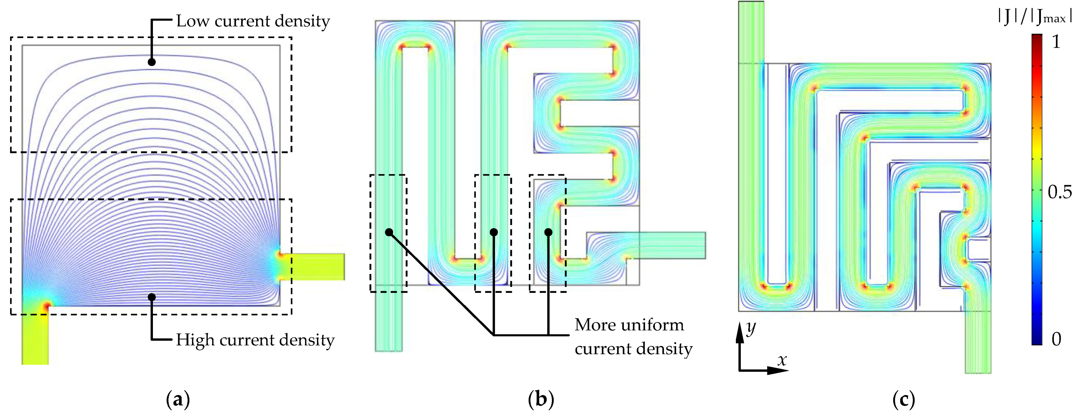
The current density distribution, calculated using finite element method (FEM), is shown in Figure 7. The simplest planar sensor made of conductive PLA is a solid rectangular plate (Figure 7a). For the contacts attached perpendicularly, the current flows mainly in the bottom area of the sensor, while much less current flows through the upper half. Since the planar sensor should measure the temperature from the entire surface, the non–uniform current distribution will lead to incorrect readings. The determined temperature is related with the measured current Ie, thus if most of the electric charge flows particularly through some area of an element, the temperature only of this area will be found. It is also worthwhile to note that the thermal conductivity of polymers with conductive fillers is still less than 2 W/mK [29], so the plate made of PLA will not behave as the thermally conductive metal. Therefore, the temperature does not have to be uniformly distributed over the surface.
To overcome these problems, a meander–type structure of considered sensors can be applied. The paths are arranged in a way so the current flows at the edges and in an inner area of the measuring surface (Figure 7b,c). The current density distribution is more uniform and as the result, the entire current Ie is directly related with the temperature distributed along the conductive path. The disadvantages of the meanders are locally higher values of the current density, observed at the vertexes of the path (red dots in Figure 7b,c). However, rounding or cutting vertexes can eliminate them.
The resistances calculated using numerical models and analytical formulae are inversely proportional to the thickness (h) and width (w) of the conductive path (Figure 8a,b), and the obtained values for both models were not identical. The analytical model assumes uniform current density along the entire conductive path, while previously discussed numerical simulations indicated divergences in the current density near the vertexes. The relative difference between numerically (Rn) and analytically (Rc) estimated reference resistances is constant with respect to the thickness (Figure 8a), e.g., ΔRc,n = 13.52% for Sensor 1 with d = 20 mm and w = s = 2 mm. However, ΔRc,n is not constant for the different widths and changes with respect to the width as well as geometry of the sensor (Figure 8c). It is worthwhile to note that for small widths (e.g., w < 0.075d) the analytical formulae may be acceptable, since the relative differences are less than 10%. Still, for the thicker paths, these differences are significant and can be even higher than 20%.

4.2. Identification of Temperature Coefficients

In Table 1, the calculated reference resistances (at Tr = 25 °C) of three printed structures were compared with the measured values. The resistances from numerical models were higher than measured; nevertheless, the relative differences were acceptable, whereas differences between theoretical and measured values were significant (ΔRc,m > 16%). Furthermore, both measurements and numerical models have shown that resistances of considered elements are not equal where, despite possessing very similar length of the meander, Sensor 2 had the highest resistance and Sensor 3 the lowest. Analytical formulae were able to indicate this variation, yet also indicated incorrect equality of resistances of Sensors 1 and 2. As the result, divergences of measured (Rm) and theoretical (Rc) reference resistances and the increasing errors for larger widths (Figure 8c), are limiting the usage of analytical formulae to initial predictions of reference resistances of relatively thin paths, while in other cases numerical models have to be utilized.
While presenting in Section 3.2 the concept of measuring an average temperature from series connected sensors, the assumption was made that Rr of sensors are equal. From Table 1, one may find that meanders do not have ideally identical resistances. However, the divergence of the reference resistances, with relation to the mean value of Rm, is less than 3%, which can be considered as an admissible value.
The Sensor 1 and Sensor 2 were additionally subjected to experimental measurements of temperature coefficients of resistance (TCR). The temperature–resistance characteristics were obtained and, based on the measured values (black dotted line in Figure 9), the coefficients of analytical models were found (Table 2). Three approximations were considered, i.e., first–order expressed by Equation (7), second–order by Equation (8) and hybrid by Equation (9). During an optimization process, the root–mean–square deviation (RMSD) between the acquired data and model was chosen as the indicator to be minimized. TCR of the linear model was 0.0087 1/°C and 0.0073 1/°C for Sensor 1 and Sensor 2, respectively, which is more than 2 times higher than TCR of, e.g., silver, copper or aluminum [30]. Moreover, in [5] the measured temperature coefficient was between 0.0036 1/°C and 0.0169 1/°C (based on sensitivity 0.1 Ω/°C and resistance 27.66 Ω at 10 °C as well as sensitivity 0.85 Ω/°C and resistance 50.28 Ω at 70 °C), so the estimated coefficient of Sensors 1 and 2 fits within this range. This indicates that conductive PLA has a sufficiently high α and can be successfully used to fabricate temperature detectors.
For the quadratic model, two coefficients were found (β and γ), where the first one was different than α and had a negative value. As the result, the second–order model should not be treated as an extension of linear model, but as a separate approximation function. Moreover, the coefficients of hybrid model were identified. While the values of α, β and γ were not significantly different for two types of sensors, the values of δ and τ were nearly identical. The hybrid model also utilizes TCR from linear model, hence it can be treated as an adequate extension of the first–order approximation.
In Figure 9, the measured characteristics and the approximations are presented. The first–order formula is valid only within some range of temperatures. According to Figure 9, a linear dependency (green solid line) is observed from 0 to less than 40 °C, where the values start to increase non–linearly. Taking into account the 5 °C margin, this range was estimated as 0 ÷ 35 °C. It follows that the linear model can be used for modeling behavior of the sensor at low temperatures.
The quadratic formula also requires the pre–imposed limit of temperatures. In this case, the temperatures ranging from 20 to 70 °C are considered. This approximation can complement the linear model in terms of modeling the resistance at high temperatures. Figure 9a,b shows that second–order model leads to major errors at the temperatures lower than Tr. Additionally, a mismatch between 50 and 60 °C appears. Obtained characteristics are consistent with observations from [5,6] where the quadratic approximation, starting from 10 to 20 °C, also had to be used. Still, the estimated limit of planar resistors linear approximation (35 °C) can be shifted. The results reported in [6,15] show, that a type of filling used in conductive filament has an impact on the linear range. For example, an application of filaments with graphene or 32.3% of carbon filler has shifted the linear range nearly to 70 °C.
The hybrid model is a combination of the linear approximation, to correctly model resistance at low temperature, and an exponential component, to model a non–linear increase in the resistance at high temperatures. The characteristics from Figure 9 (red solid line) are nearly perfectly fitted to measured data within the entire range of the considered temperatures. Hence, the hybrid approach can be used as a more versatile method of modeling of the temperature detectors based on conductive PLA.

4.3. Average Temperature Measurement

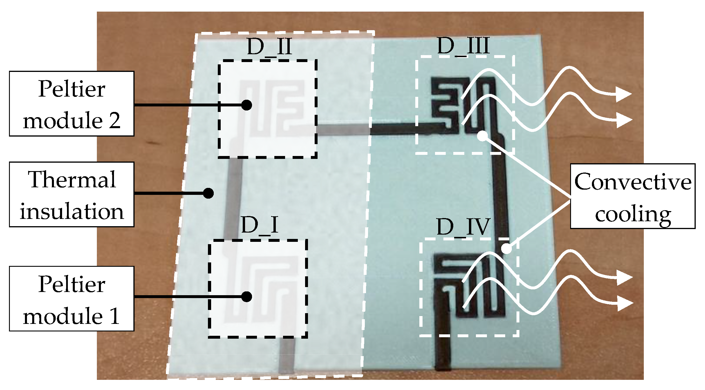
To validate a concept of measuring an average temperature, a planar device consisting of four sensors and a flexible insulating substrate was 3D printed (Figure 10). Elements were connected using short paths (1 mm thick), printed of conductive PLA. Each detector had identical geometrical parameters as previously discussed Sensor 1 and Sensor 2. Before proceeding to the main experiments, the resistances of detectors and connections were found. A mean value of the reference resistance of a single sensor was Re = 5.565 kΩ, while a quarter of the total resistance of connecting paths was Rp = 0.847 kΩ (Tr = 25 °C and α = 0.0087 1/°C). Then, Equation (12) was used to calculate the average temperature Ta, where it was assumed that Rr = Re + Rp.
To perform the measurements Peltier modules were attached to detectors D_I and D_II. The left half was insulated using polystyrene, while the right half was left open to ensure a convective cooling of elements D_III and D_IV. The temperature was measured at the center of each sensor using a thermocouple. Three cases were considered (Table 3). In Case 1, the highest possible temperature of 35 °C (at which the linear approximation is valid) and much lower temperature (11 °C) were applied, to create a high gradient of temperatures. In Case 2, the opposite situation was considered, where the values of temperatures at different detectors are similar. Meanwhile, in Case 3, the possibility of averaging low temperatures and the room temperature was tested.
The mean values of temperatures (Tavg) were measured by a thermocouple and listed in Table 3. The Case 1 and Case 2 were designed to have similar values of Tavg and verify, if the two–port measurement will be able to provide a correct value of the average temperature, despite small differences. The results in Table 4 shows that calculated average temperature (Ta) was correct in Case 2 (relative difference less than 1%). In Case 1, the difference was more significant (7.66%); however, a derived value of Ta (21.47 °C) was still close to the exact value (23.25 °C).
Good agreement was also found in Case 3, where relative difference was 1.08%, so the estimated temperature differed from the exact by 0.16 °C. In each case, the qualitative agreement was preserved, since measurements indicated lower average temperature in Case 1 compared to Case 2, while the lowest temperature was found in Case 3.

5. Conclusions

The novel planar resistance temperature detectors were proposed. It was shown that using commercially available printer and filaments, it is possible to 3D print sensors, which are able to measure the temperature at specific surfaces. Three types of elements, characterized by identical resistance but different internal geometry and position of contacts, were introduced. Due to a thin shape, the usage of flexible filament and meander–shaped conductive paths, it was possible to create elastic elements, which can be easily scaled and adjusted to specific applications.
The numerical models of detectors were presented along with the resulting analysis of the current density distribution. The results have shown that a solid conductive plate was not able to provide the uniform current flow through its structure, while a conductive path distributed over the measuring surface have overcome this problem. The numerical simulations have proven that proposed elements have approximately the same resistance, yet different than those estimated analytically. Still, analytical formulae for the reference resistance and the first–order temperature dependence of the resistance at low temperatures, may be used to model the properties of planar sensors with thin paths.
The sensors were tested experimentally and the temperature coefficients were estimated. The conducted research has indicated a linear temperature dependence of resistance from 0 to 35 °C, while for higher temperatures this dependency was non–linear, hence a second–order approximation should be utilized. Nonetheless, the entire range of temperatures was correctly modeled by the hybrid approximation, where both linear part at low temperatures and non–linear increase at high temperatures were accurately represented. Finally, a device consisting of four sensors was used to determine a mean value of temperatures. The results have shown that, using presented approach, the average temperature was found with the acceptable accuracy.

Author Contributions

Conceptualization, A.S. and K.K.; methodology, A.S.; validation, A.S. and J.M.S.; formal analysis, A.S. and K.K.; investigation, K.K.; data curation, K.K. and A.C.; writing—original draft preparation, A.S.; writing—review and editing, A.C. and J.M.S.; supervision, A.C.; funding acquisition, A.C. and J.M.S. All authors have read and agreed to the published version of the manuscript.

Funding

This research was funded by the Ministry of Science and Higher Education in Poland at the Bialystok University of Technology under research subsidy No. WZ/WE–IA/2/2020.

Conflicts of Interest

The authors declare no conflict of interest.

References

  1. Rayna, T.; Striukova, L. From rapid prototyping to home fabrication: How 3D printing is changing business model innovation. Technol. Soc. Chang. 2016, 102, 214–224. [Google Scholar] [CrossRef] [Green Version]
  2. Macdonald, E.; Salas, R.; Espalin, D.; Perez, M.; Aguilera, E.; Muse, D.; Wicker, R.B. 3D Printing for the Rapid Prototyping of Structural Electronics. IEEE Access 2014, 2, 234–242. [Google Scholar] [CrossRef]
  3. Asnafi, N.; Shams, T.; Aspenberg, D.; Oberg, C. 3D Metal Printing from an Industrial Perspective—Product Design, Production, and Business Models. Berg. Huettenmaenn Mon. 2019, 164, 91–100. [Google Scholar] [CrossRef] [Green Version]
  4. Nguyen, N.D.; Ashraf, I.; Kim, W. Compact Model for 3D Printer Energy Estimation and Practical Energy–Saving Strategy. Electronics 2021, 10, 483. [Google Scholar] [CrossRef]
  5. Marasso, S.L.; Cocuzza, M.; Bertana, V.; Perrucci, F.; Tommasi, A.; Ferrero, S.; Scaltrito, L.; Pirri, C.F. PLA conductive filament for 3D printed smart sensing applications. Rapid Prototyp. J. 2017, 24, 739–743. [Google Scholar] [CrossRef]
  6. Kwok, S.W.; Goh, K.H.H.; Tan, Z.D.; Tan, S.T.M.; Tjiu, W.W.; Soh, J.Y.; Ng, Z.J.G.; Chan, Y.Z.; Hui, H.K.; Goh, K.E.J. Electrically conductive filament for 3D–printed circuits and sensors. Appl. Mater. Today 2017, 9, 167–175. [Google Scholar] [CrossRef]
  7. Lee, J.; Kwon, H.; Seo, S. Conductive fiber–based ultrasensitive textile pressure sensor for wearable electronics. Adv. Mater. 2015, 27, 2433–2439. [Google Scholar] [CrossRef]
  8. Wang, Z.; Gao, W.; Zhang, Q.; Zheng, K.; Xu, J.; Shang, E.; Jiang, J.; Zhang, J.; Liu, Y. 3D Printed Graphene/PDMS Composites for Stretchable and Strain–Insensitive Temperature Sensors. ACS Appl. Mater. Interfaces 2019, 11, 1344–1352. [Google Scholar] [CrossRef] [PubMed]
  9. Arbaoui, Y.; Agaciak, P.; Cevelier, A.; Laur, V.; Maalouf, A.; Ville, J.; Roquefort, P.; Aubry, T.; Queffelec, P. 3D printed ferromagnetic composites for microwave applications. J. Mater. Sci. 2017, 52, 4988–4996. [Google Scholar] [CrossRef]
  10. Khosravani, M.R.; Reinicke, T. 3D–printed sensors: Current progress and future challenges. Sens. Actuator A Phys. 2020, 305, 111916. [Google Scholar] [CrossRef]
  11. Zhu, Z.; Park, H.S.; McAlpine, M.C. 3D printed deformable sensors. Sci. Adv. 2020, 6, eaba5575. [Google Scholar] [CrossRef]
  12. Han, T.; Kundu, S.; Nag, A.; Xu, Y. 3D Printed Sensors for Biomedical Applications: A Review. Sensors 2019, 19, 1706. [Google Scholar] [CrossRef] [PubMed] [Green Version]
  13. Zhao, J.; Zhang, Y.; Huang, Y.; Xie, J.; Zhao, X.; Li, C.; Qu, J.; Zhang, Q.; Sun, J.; He, B.; et al. 3D Printing Fiber Electrodes for an All–Fiber Integrated Electronic Device via Hybridization of an Asymmetric Supercapacitor and a Temperature Sensor. Adv. Sci. 2018, 5, 1801114. [Google Scholar] [CrossRef]
  14. Su, Y.; Ma, C.; Chen, J.; Wu, H.; Luo, W.; Peng, Y.; Luo, Z.; Li, L.; Tan, Y.; Omisore, O.M.; et al. Printable, Highly Sensitive Flexible Temperature Sensors for Human Body Temperature Monitoring: A Review. Nanoscale Res. Lett. 2020, 15, 200. [Google Scholar] [CrossRef]
  15. Sajid, M.; Gul, J.Z.; Kim, S.W.; Kim, H.B.; Na, K.H.; Choi, K.H. Development of 3D–Printed Embedded Temperature Sensor for Both Terrestrial and Aquatic Environmental Monitoring Robots. 3D Print. Addit. Manuf. 2018, 5, 160–169. [Google Scholar] [CrossRef]
  16. Sommer, L.; Ramachandran, R.P. Untreated Low Cost Inkjet Printed Temperature Sensors–Conditionally Suitable? Int. J. Appl. Eng. Res. 2018, 13, 5626–5632. [Google Scholar]
  17. Vlachakis, C.; Perry, M.; Biondi, L.; McAlorum, J. 3D printed temperature–sensing repairs for concrete structures. Addit. Manuf. 2020, 34, 101238. [Google Scholar] [CrossRef]
  18. Li, R.; Smith, A.A.; Tadinada, H.S.; Tse, Z.T.H. Heatguard: An Ultra–Low–Cost 3D Printed Sensor for Body Temperature Alert & Reporting System. In Proceedings of the 2018 Design of Medical Devices Conference DMD2018, Minneapolis, MN, USA, 9–12 April 2018. [Google Scholar]
  19. Xin, Y.; Zhou, J.; Lubineau, G. A highly stretchable strain–insensitive temperature sensor exploits the Seebeck effect in nanoparticlebased printed circuits. J. Mater. Chem. A 2019, 7, 24493. [Google Scholar] [CrossRef] [Green Version]
  20. Ota, H.; Emaminejad, S.; Gao, Y.; Zhao, A.; Wu, E.; Challa, S.; Chen, K.; Fahad, H.M.; Jha, A.K.; Kiriya, D.; et al. Application of 3D Printing for Smart Objects with Embedded Electronic Sensors and Systems. Adv. Mater. Technol. 2016, 1, 1600013. [Google Scholar] [CrossRef] [Green Version]
  21. Fuketa, H.; Hamamatsu, M.; Yokota, T.; Yukita, W.; Someya, T.; Sekitani, T.; Takamiya, M.; Someya, T.; Sakurai, T. Energy–Autonomous Fever Alarm Armband Integrating Fully Flexible Solar Cells, Piezoelectric Speaker, Temperature Detector, and 12V Organic Complementary FET Circuits. In Proceedings of the 2015 IEEE International Solid–State Circuits Conference—(ISSCC) Digest of Technical Papers, San Francisco, CA, USA, 22–26 February 2015. [Google Scholar]
  22. Sauerbrunn, E.; Chen, Y.; Didion, J.; Yu, M.; Smela, E.; Bruck, H.A. Thermal imaging using polymer nanocomposite temperature sensors. Phys. Status Solidi A 2015, 212, 2239–2245. [Google Scholar] [CrossRef]
  23. Wang, G.; Cheng, T.; Do, Y.; Yang, H.; Tao, Y.; Gu, J.; An, B.; Yao, L. Printed Paper Actuator: A Low–cost Reversible Actuation and Sensing Method for Shape Changing Interfaces. In Proceedings of the 2018 CHI Conference on Human Factors in Computing Systems CHI ‘18, Montreal, QC, Canada, 21–26 April 2018. [Google Scholar]
  24. Steckiewicz, A.; Choroszucho, A. Optimization–based synthesis of a metamaterial electric cloak using nonhomogeneous composite materials. J. Electromagn. Waves Appl. 2019, 33, 1933–1941. [Google Scholar] [CrossRef]
  25. Kasap, S.O. Principles of Electronic Materials and Devices; McGraw–Hill: Boston, MA, USA, 2006; pp. 127–129. [Google Scholar]
  26. NinjaFlex 3D Printing Filament. Flexible Polyurethane Material for FDM Printers. Available online: https://ninjatek.com/wp–content/uploads/2019/10/NinjaFlex–TDS.pdf (accessed on 20 March 2021).
  27. Proto–Pasta Technical Data Sheet Rev 1. Conductive PLA. Available online: https://cdn.shopify.com/s/files/1/0717/9095/files/TDS__Conductive_PLA_1.0.1.pdf (accessed on 20 March 2021).
  28. FormFutura Technical Data Sheet. Product Name: ApolloX. Available online: https://formfutura.sharepoint.com/sites/downloads/Shared%20Documents/Downloads%20Server/Materials/Filaments/FormFutura%20Filaments/ApolloX/Data%20Sheets%20and%20Declarations/TDS%20–%20ApolloX.pdf (accessed on 20 March 2021).
  29. Ngo, I.-L.; Jeon, S.; Byon, C. Thermal conductivity of transparent and flexible polymers containing fillers: A literature review. Int. J. Heat Mass Transf. 2016, 98, 219–226. [Google Scholar] [CrossRef]
  30. Olivia, A.I.; Lugo, J.M. Measurement of the Temperature Coefficient of Resistance in Metallic Films with Nano–thickness. Int. J. 2016, 37, 35. [Google Scholar] [CrossRef]
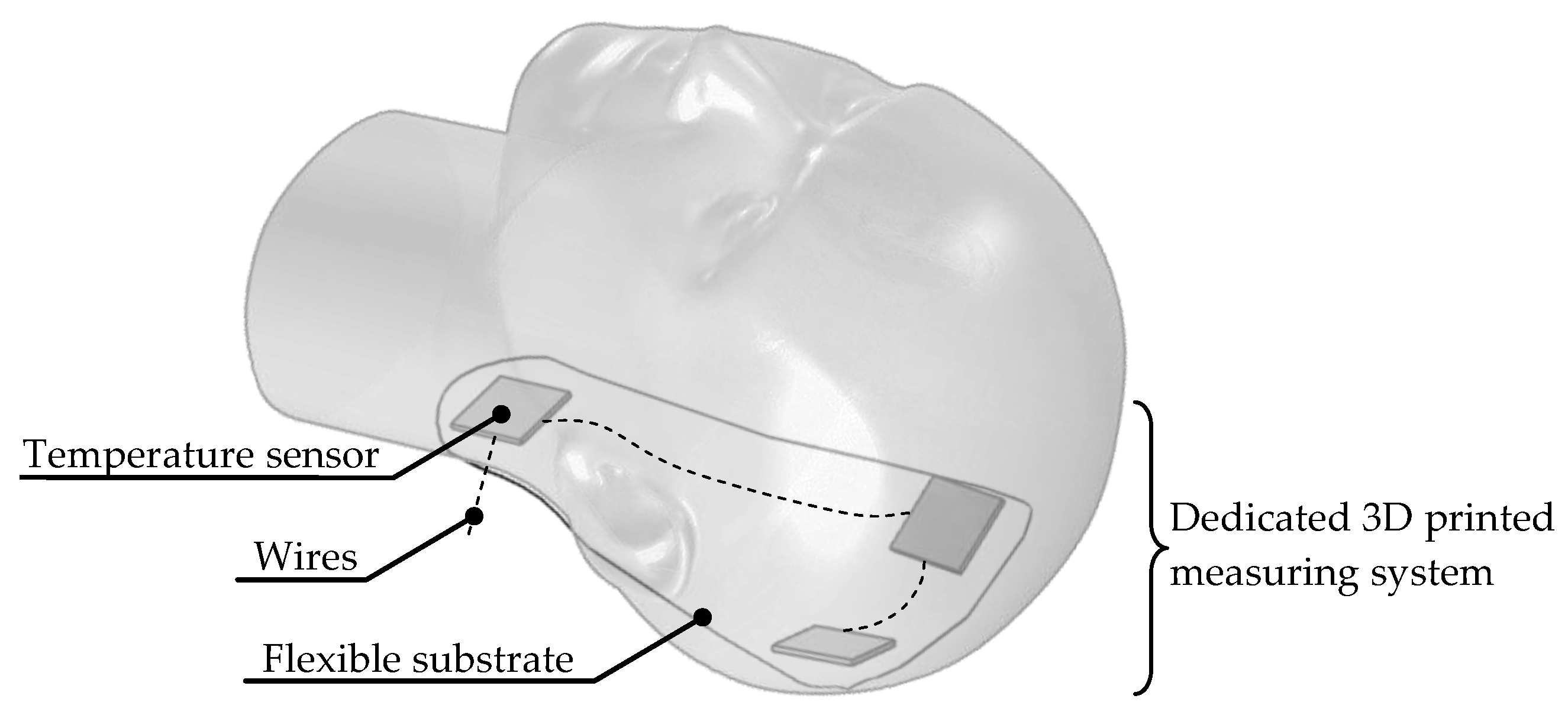
Figure 1. An exemplary application of 3D printed surfaces with planar sensors embedded in a flexible substrate, dedicated to individual needs and purposes.
Electronics 10 01100 g001
Figure 2. The proposed structures of surface temperature detectors: (a) composition of the structure with perpendicular contacts, (b) sensor with shifted parallel contacts and (c) sensor with centered parallel contacts.
Electronics 10 01100 g002
Figure 3. The printed temperature detectors: (a) sensor with perpendicular contacts, (b) sensor with parallel contacts and (c) rectangular surface with four sensors embedded in a flexible substrate.
Electronics 10 01100 g003
Figure 4. The series connection of several temperature sensors used for a measurement of an average temperature.
Electronics 10 01100 g004
Figure 5. The main steps of printing procedure: (a) forming a flexible base, (b) adding the conductive paths and (c) finalizing the print (a raft in upper right corner was used for cleaning the print heads during the operation).
Electronics 10 01100 g005
Figure 6. The miniaturized version of a temperature chamber used as an experimental stand: (a) a general view on the set and (b) the stand and samples prepared for the measurements.
Electronics 10 01100 g006
Figure 7. The relative current density distribution: (a) solid plate made of conductive PLA, (b) sensor with perpendicular contacts (Sensor 1) and (c) sensor with parallel contacts (Sensor 2).
Electronics 10 01100 g007
Figure 8. Numerically and analytically calculated: (a) the reference resistance of Sensor 1 for different thicknesses of the path at d = 20 mm and w = 2 mm, (b) the reference resistance of Sensor 1 for different widths of the path at d = 20 mm and h = 0.5 mm and (c) relative differences between numerical and analytical results for three sensors.
Electronics 10 01100 g008
Figure 9. The measured and approximated by analytical models temperature dependence of the resistance for: (a) the Sensor 1 and (b) the Sensor 2.
Electronics 10 01100 g009
Figure 10. The configuration to determine an average temperature of a four–sensor device.
Electronics 10 01100 g010
Table 1. Measured (Rm), numerically (Rn) and analytically (Rc) calculated reference resistances, and the relative differences (ΔR) for three sensors with d = 20 mm, w = s = 2 mm, h = 0.5 mm.
SensorRm (kΩ)Rn (kΩ)ΔRn,mRc (kΩ)ΔRc,m
15.695.974.80%6.7719.01%
25.836.074.05%6.7716.12%
35.515.856.18%6.6620.77%
Table 2. Optimal values of approximation coefficients and corresponding RMSD of three models.
Modelα (1/°C)β (1/°C)γ (1/°C2)δ (–)τ (1/°C)RMSD (°C)
1st order, Sensor 10.00870.174
2nd order, Sensor 1−0.020720.002271.153
Hybrid, Sensor 10.00870.04620.09640.269
1st order, Sensor 20.00730.125
2nd order, Sensor 2−0.011910.001810.668
Hybrid, Sensor 20.00730.04640.09250.206
Table 3. The temperatures set on the individual elements.
DetectorCase 1Case 2Case 3
D_I35.0 °C26.0 °C9.0 °C
D_II11.0 °C21.5 °C4.0 °C
D_III24.0 °C23.5 °C22.0 °C
D_IV23.0 °C23.5 °C23.0 °C
Table 4. The measured series resistances (Rs), calculated mean temperatures (Ta) and measured average temperatures (Tavg).
ParameterCase 1Case 2Case 3
Rs (kΩ)24.8625.2923.27
Ta (°C)21.4723.4014.34
Tavg (°C)23.2523.6314.50
ΔT = |TaTavg|/Tavg7.66%0.97%1.08%
Publisher’s Note: MDPI stays neutral with regard to jurisdictional claims in published maps and institutional affiliations.