Article

Failure Rate and Economic Cost Analysis of Clamped-Single Submodule with DC Short Current Protection for High Voltage Direct Current System

1
Department of Electronic Engineering, Hanbat National University, Daejeon 34158, Korea
2
Energy Conversion Research Centre, Korea Electronics Technology Institute, Gwangju 61011, Korea
*
Author to whom correspondence should be addressed.
Electronics 2021, 10(9), 993; https://doi.org/10.3390/electronics10090993
Submission received: 18 March 2021 / Revised: 18 April 2021 / Accepted: 19 April 2021 / Published: 21 April 2021
(This article belongs to the Section Power Electronics)

Abstract

:
Clamped-single submodule (CSSM) has DC short circuit current protection function to improve the safety and stability of high voltage, direct current (HVDC) system. In order to carry out the protection, it needs an additional number of insulated gate bipolar transistors (IGBTs) and diodes compared to the conventional half-bridge submodule (HBSM). In general, the failure rate tends to increase in proportion to the number of circuit components. Also, complex operation of the submodule may increase the failure rate, so accurate reliability analysis considering these points is required to apply CSSM in a practical HVDC system. We estimate the failure rate and the mean time between failures (MTBF) of CSSM using a fault tree. Fault-tree analysis (FTA) is possible to analyze the failure rate more accurately than the prior part count failure analysis (PCA) that considers only the number of parts, the type of parts, and the connection status of each circuit component. To provide guidelines for submodule selection under various conditions, we compare the economic cost of a CSSM with HBSM, FBSM, and clamped-double submodule (CDSM), and analyze the failure rate according to the voltage margin of the parts.

1. Introduction

Half and full-bridge structures are widely used for HVDC submodules [1,2,3,4,5,6,7]. The submodule, which is composed of multiple stages for high voltage and high current application purposes, is an important factor in determining the reliability of the HVDC system. Modular multilevel converter (MMC), in which multiple submodules are used in a series-parallel combination, can sufficiently improve reliability due to redundancy by using extra submodules. However, the submodule itself has no protection function against DC short current, which causes overvoltage and capacitor voltage rise. To alleviate this problem, submodules with DC short circuit current protection were introduced [8,9,10,11]. Clamped-double submodule (CDSM) was introduced in [8]. It adds one IGBT, two diodes, and a capacitor to the full-bridge structure. When a DC short circuit current occurs, CDSM bypasses the fault current through the capacitor to absorb short current energy and prevents overvoltage by clamping the voltage through the diode. However, in order to protect the submodule from DC short current, the IGBT is kept in a turned-on state, so large conduction losses occur, and switching losses are increased because of the tailing current of IGBT [9]. Most of all, when the number of parts increases and the operation becomes complicated, the failure rate is increased as usual. The improved hybrid submodule (IHSM) was introduced to reduce the number of circuit components while suppressing the effects of DC short current through capacitors and diodes [10]. IHSM can effectively solve the problems caused by DC short current. Moreover, IHSM reduces the number of diodes compared to CDSM. However, the IGBT was turned on all the time, so the problem of the same loss as CDSM and the high component failure rate was not solved. The submodule circuit configuration given in [11] is a combination of three IGBTs in series and added the function of protection against DC short circuit current. It can be seen that it is advantageous in the number of parts because this circuit topology just adds one IGBT and one diode to the half-bridge submodule. In general, as the number of parts increases, the failure rate increases, and it means that the reliability of the submodule decreases. However, when the DC short current protection function is added, it has the effect of suppressing the increase of the failure rate due to the increase in the number of parts.
In this paper, we analyze the failure rate of CSSM that has a DC short current protection function but has a relatively small number of components. Here we focus on analyzing how the DC short current protection function and the number of components affect the failure rate. The results are compared to conventional HBSM, FBSM, and CDSM. To analyze the effect of the DC short current protection function on the failure rate, a failure rate analysis using a fault tree is performed. Fault-tree analysis (FTA) enables a stochastic quantitative assessment of the risk of submodule operation. Therefore, it is possible to derive logical and probabilistic quantitative results by deviating from previous empirical thinking [12,13,14,15,16,17,18,19,20]. The failure rate according to the DC short current protection function of CSSM can be found by comparing the FTA results with the traditional PCA (part count analysis) results. We compare the failure rate of HBSM, FBSM, CDSM, and CSSM with the number of components, voltage, and current stress of the switching devices, and analyze the failure rate according to the voltage rating margin. This paper can serve as a guideline for selecting HVDC submodules by judging the reliability and economic cost of submodules employing DC short current protection.

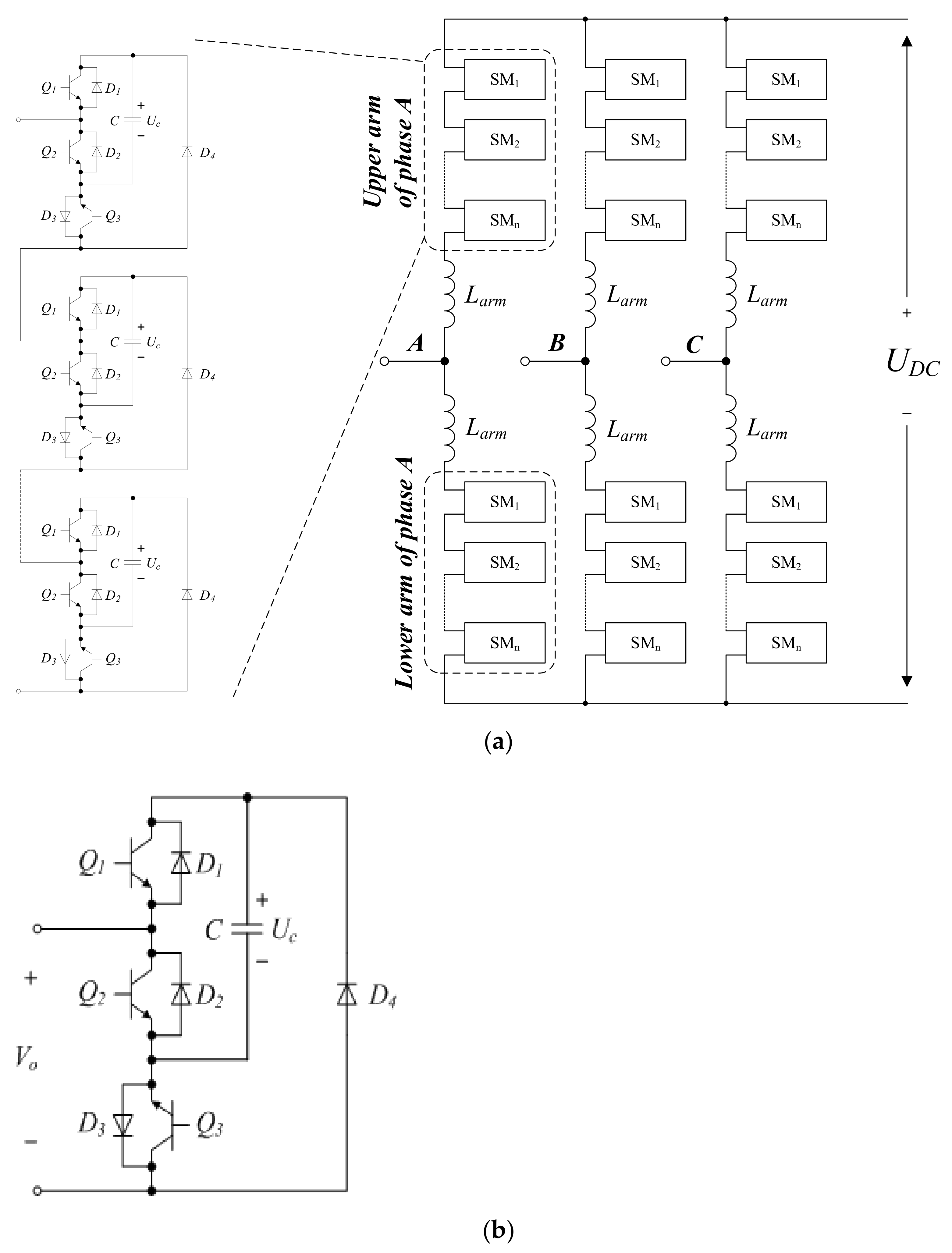
2. Clamped-Single Submodule

This chapter analyzes the driving characteristics of the clamped-single submodule (CSSM) employing DC short current protection. Figure 1a shows a circuit configuration of a modular multilevel converter (MMC) consisted of clamped-single submodules. CSSM is a circuit structure that implements DC short current protection by adding one IGBT in series with the half-bridge switch arm and one diode with the outermost loop. Since one additional diode clamps the capacitor voltage, the term clamped-single is used. When a DC short current occurs, it is possible to minimize overvoltage and absorb energy by creating a current path through the capacitor with bidirectional current flow.

2.1. Operational Mode

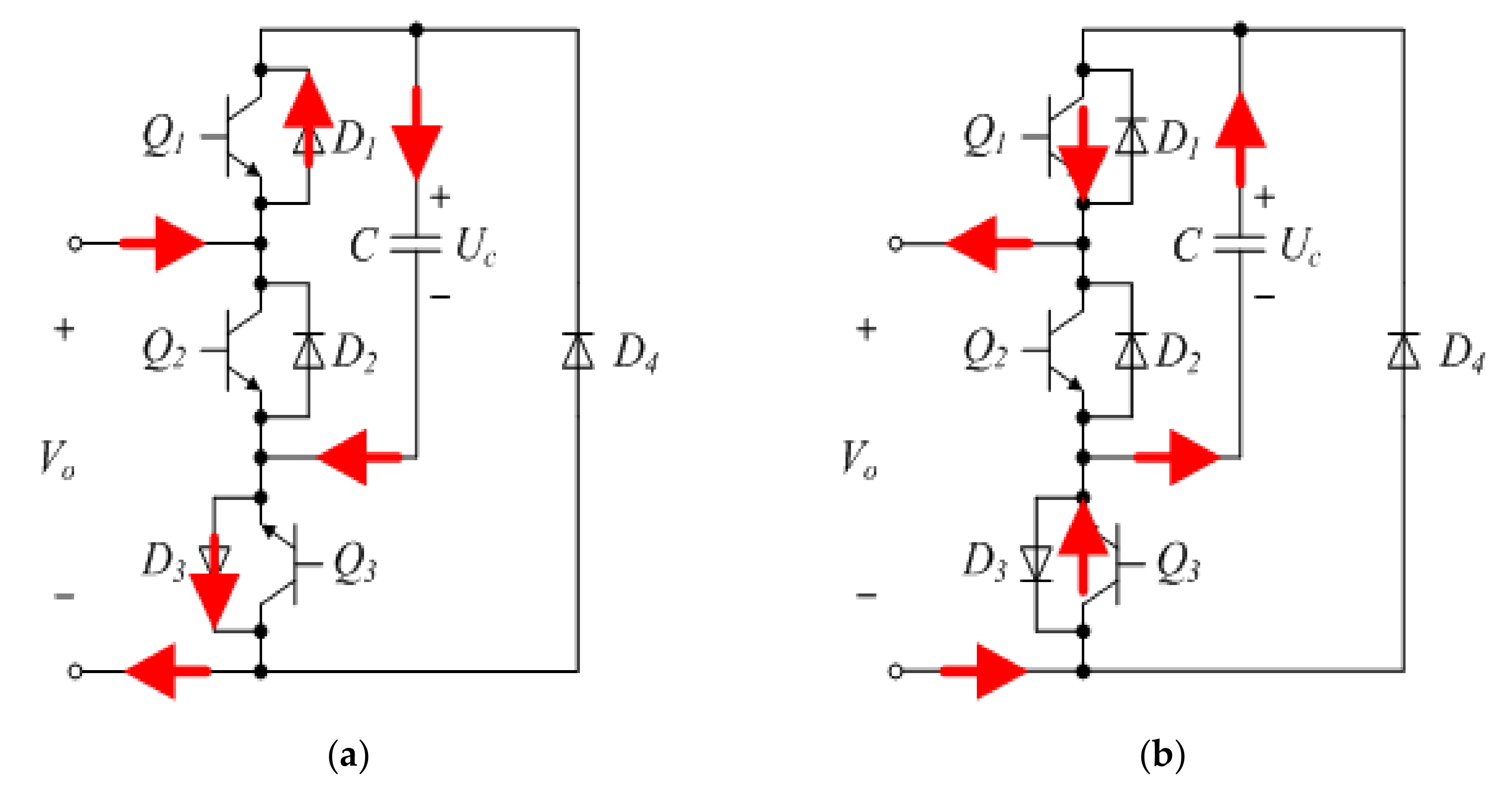
2.1.1. Normal Operation Mode at Connected to Converter

Figure 2a shows the equivalent circuit for two current paths of CSSM in a normal operation mode in case that CSSM is connected to the converter. When the current flows into the (+) terminal of the submodule, the capacitor is charged through diodes D1 and D3, and if discharge of the capacitor is required, a current path is formed through turn-on control of IGBT Q1 and Q3. In normal operation mode, IGBT Q2 serves to separate Q1 and Q3, and diode D4 serves to clamp the voltage of the capacitor.

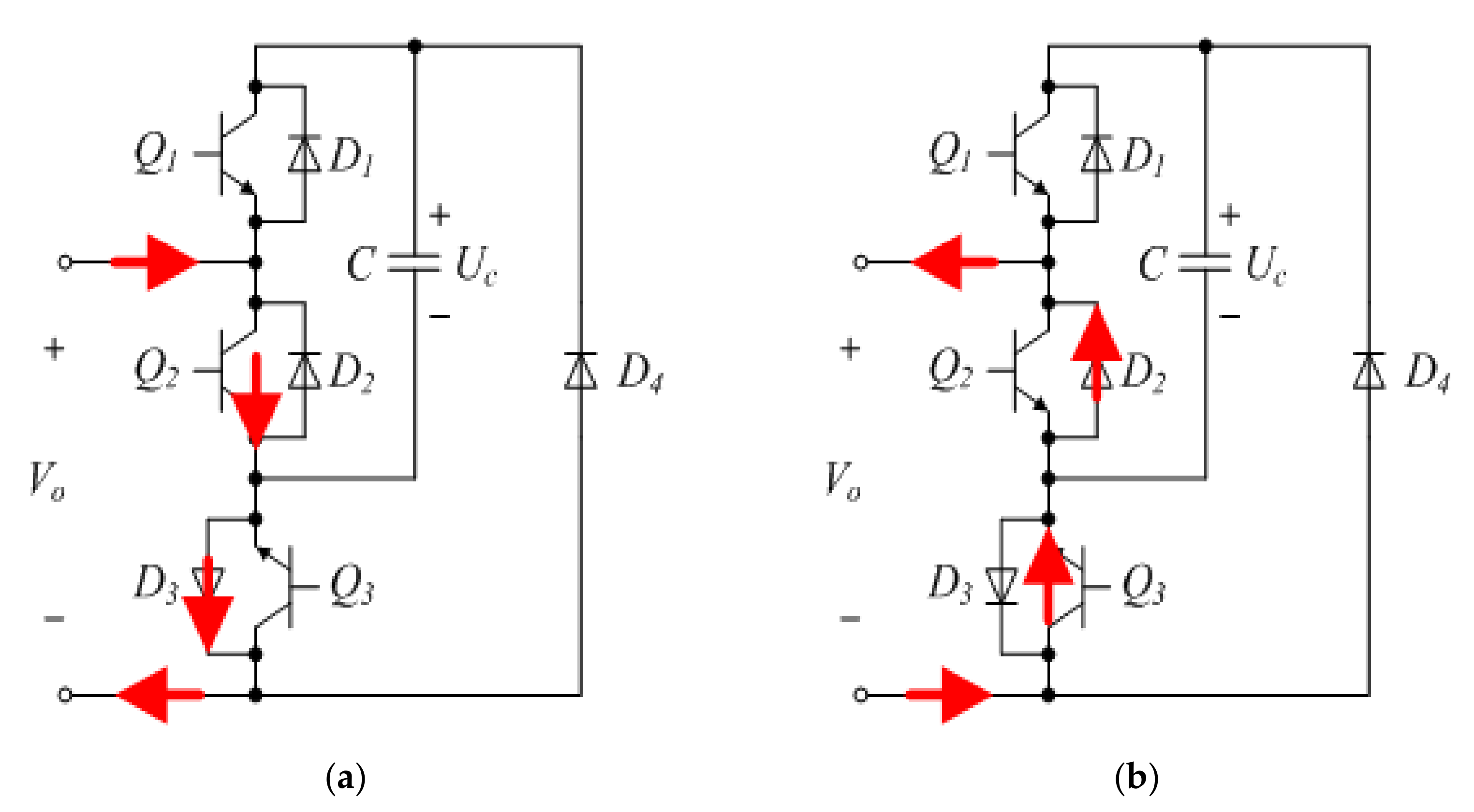
2.1.2. Normal Operation Mode at Disconnected to Converter

Figure 3 shows the equivalent circuit for two bypass modes of CSSM separated from the converter in normal operation mode. When the current is flowing into the (+) terminal of the submodule, it bypasses through IGBT Q2 and diode Q3 as shown in Figure 3a. When the current is flowing out of the (+) terminal of the submodule, the converter and submodule can be separated by bypassing the current through IGBT Q3 and diode Q2 as shown in Figure 3b.

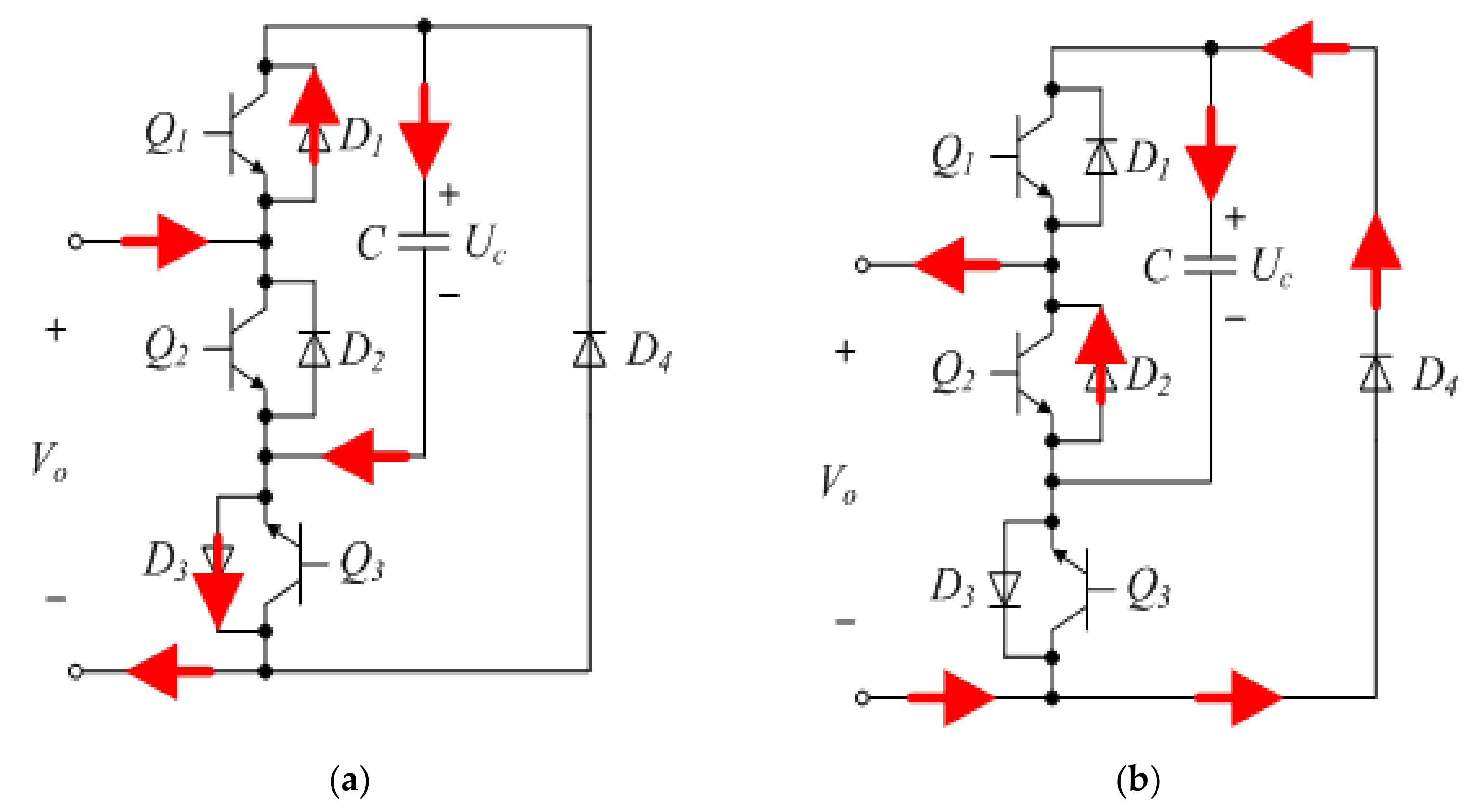
2.1.3. Abnormal Operation Mode

Figure 4 shows the circuit state of CSSM in abnormal operation mode, in which DC short current occurs. Two current paths can be expected depending on the direction in which the DC short current flows into or out of the submodule. Since the DC short current passes through the capacitor, the energy generated by the short current is absorbed by the capacitor and the voltage is clamped by the diode D4 to activate the protection function to prevent overvoltage. CSSM is expected to be superior in reliability compared to the conventional half-bridge submodule (HBSM) by adding DC short current protection. However, the added IGBT and diode will increase the cost, and switching losses and conduction losses will decrease the efficiency.

2.2. Design Consideration

Table 1 shows the design parameters of CSSM. For an accurate comparison, the same values as the design parameters of the existing submodules are applied [6,9]. The voltage and current ratings of IGBTs are 4.5 kV and 1200 A. The junction temperature of the IGBT and heat sink is designed at 125 °C. Instead of the internal body diode of IGBT, it uses a high-performance fast recovery diode, and its voltage and current ratings are the same as those of IGBT. The operating temperature of the capacitor is −40~85 °C, the operating voltage is 2160~2640 V, and the rated voltage is 2750 V in continuous operation. Reliability analysis is performed in an environment where the temperature of the converter room is controlled by 20~30 °C by the air conditioning system.

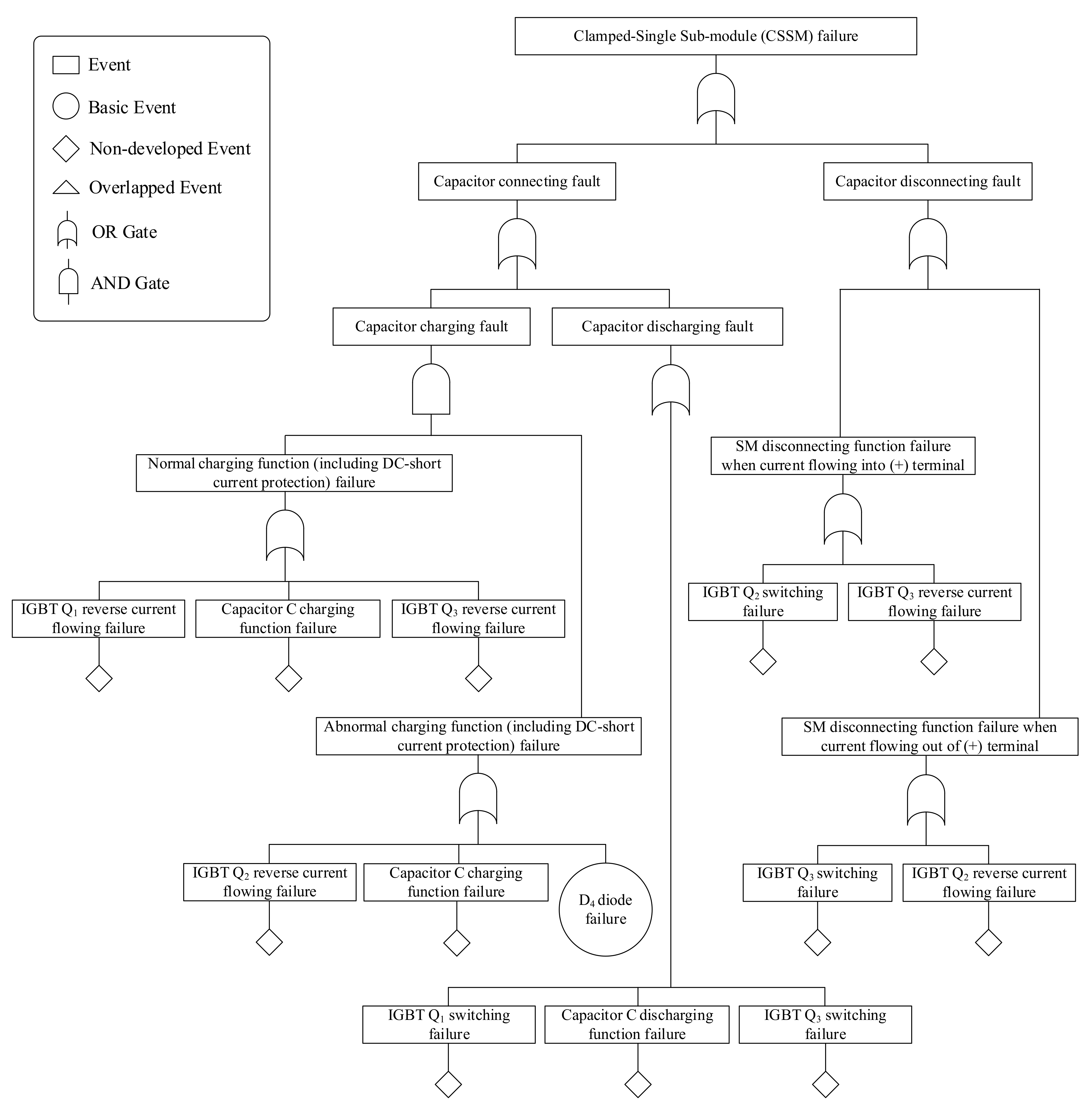
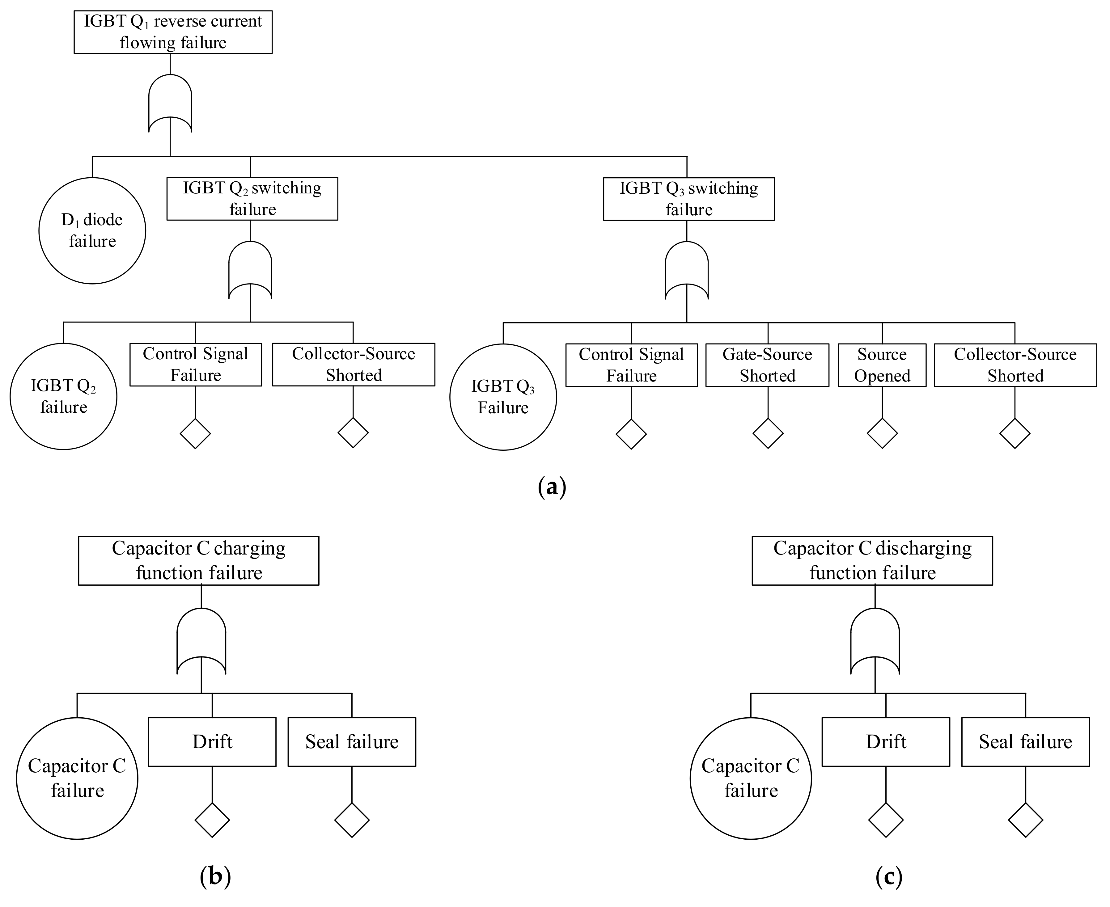
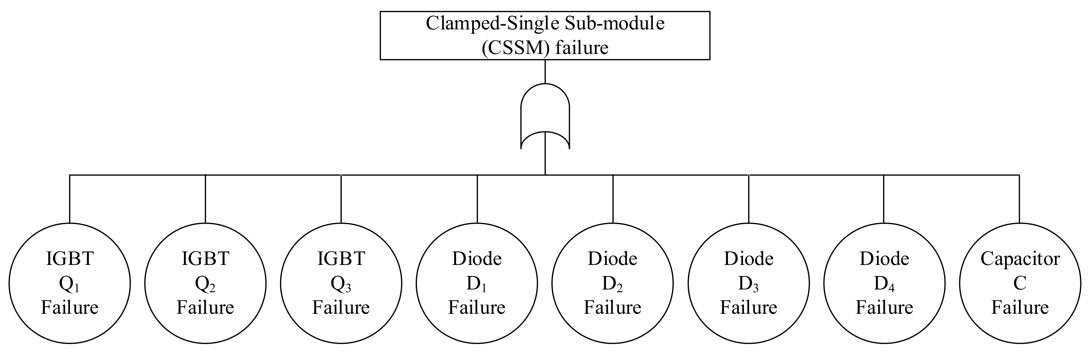
3. Failure Rate Analysis of CSSM

FTA is a quantitative failure analysis-based reliability evaluation method that logically analyzes the cause of system failures to design fault trees and improve the reliability of the system by finding the probability of failure. By enabling stochastic quantitative assessments of the operational risks of submodules, it can deviate from the method of evaluating reliability based on previous sensory and empirical thinking. The FTA uses Boolean algebra to express the top to bottom events in a top-down way, and the fault-tree is designed with a focus on the function of the submodule. Although the failure rate of the submodule may vary depending on the designer’s failure analysis method or fault library difference, the FTA has the advantage of analyzing the failure rate considering the risk of submodule operation. On the other hand, conventional PCA methods cannot consider the risk of submodule operation or behavioral characteristics that improve reliability, such as DC-short current protection, by analyzing failure rates only by considering the type of parts, the number of parts, and connection between parts [12,13,14,15,16,17,18,19,20].

3.1. Fault-Tree Design Considering Operational Risk

Figure 5 shows the main fault tree, considering the driving characteristics of CSSM. Each sub-fault is defined based on the condition that the capacitor is connected or disconnected from the converter. ‘Capacitor connecting failure’ is designed to be divided into a failure in the state of capacitor charging fault and a failure in the state of discharging capacitor. ‘Capacitor charging fault’ is designed by an AND-gate combination of ‘Normal charging function (including DC-short current protection) failure’ and ‘Abnormal charging function (including DC-short current protection) failure’. When a DC short current occurs, a current path in which the capacitor absorbs the short current is formed, and the failure propagates to a higher level only when a failure of all events occurs. ‘Capacitor discharging fault’ can be implemented with only one current path in normal operation mode. Therefore, if one of the events of ‘IGBT Q1 switching failure’, ‘Capacitor C discharging function failure’, or ‘IGBT Q3 switching failure’ fails, it is designed as an OR-gate combination that propagates to a higher-level failure.
‘Capacitor disconnecting failure’ is a state that separates the capacitor and converter of the submodule and is designed by dividing into two states in which current flows into and out of the submodule (+) terminal. ‘SM disconnecting function failure when the current flowing into (+) terminal’ is a state in which current flows into the submodule (+) terminal when separating the submodule from the converter. It is designed by OR-gate combining ‘IGBT Q2 switching failure’ and ‘IGBT Q3 reverse current flowing failure’. ‘SM disconnecting function failure when the current flowing out of (+) terminal’ is a state in which current flows from the submodule (+) terminal to the converter when separating the submodule from the converter. It is designed as an OR-gate combination of ‘IGBT Q3 switching failure’ and ‘IGBT Q2 reverse current flowing failure’.
Figure 6a shows sub fault-tree for the ‘IGBT Q1 reverse current flowing failure’ event. It is designed by OR-gate combination of ‘D1 diode failure’, ‘IGBT Q2 switching failure’, and ‘IGBT Q3 switching failure’. CSSM consists of three IGBTs in series. Therefore, although the current is flowing through diode D1, a failure may occur due to the switching error of IGBT Q2 and Q3. At this time, in case of being located at the edge such as IGBT Q3, in addition to IGBT’s failure and switching signal error, ‘Gate-Source Shorted’, ‘Source Opened’, ‘Collector-Source Shorted’ failure is considered, and in the case of centrally located IGBT Q2 considers only the ‘Collector-Source Shorted’ fault. ‘Capacitor C charging function failure’ and ‘Capacitor C discharging function failure’ in Figure 6b,c are designed as sub-failures of the capacitor itself and frequent ‘Drift’ and ‘Seal failure’ among major failures of the capacitor. In Figure 6d, ‘IGBT Q3 reverse current flowing failure’ is represented by the duality of diodes D3 and D1 and IGBT Q3 and Q1 in Figure 6a. Figure 6e shows the sub fault-tree of ‘IGBT Q2 reverse current flowing failure’. It is designed by OR-gate combination of ‘D2 diode failure’, ‘IGBT Q3 switching failure’, and ‘IGBT Q1 switching failure’. CSSM consists of three IGBTs in series, so if current flows through diode D2, a failure may occur due to switching errors of IGBT Q1 and Q3. Since IGBT Q1 and Q3 are located at the edge, IGBT’s own failure ‘IGBT Qx Failure’ and switching signal error ‘Control Signal Failure’ are the main causes of failure. Additionally, the cause of failure of ‘Gate-Source Shorted’, ‘Source Opened’, and ‘Collector-Source Shorted’- is considered as shown in Figure 6e.

3.2. Calculation of Part Failure Rates Based on MIL-HDBK-217F

To calculate the failure rate of a submodule, we first need to calculate the failure rate of the main components: IGBTs, diodes, and capacitors. Here, the part failure rate is calculated using the fault library of MIL-HDBK-217F [21,22,23].

3.2.1. Failure Rate of IGBT

The IGBT failure rate is calculated by OR-gate combination of bipolar junction transistor (BJT) and metal oxide semiconductor field effect transistor (MOSFET) failure rate provided by MIL-HDBK-217F as given in (3) [24,25].
λ p _ B J T = λ b π T π A π R π S π Q π E   Failures / 10 6   h
λ P _ M O S F E T = λ b π T π A π Q π E   Failures / 10 6   h
λ P _ I G B T = 1 ( 1 λ P _ B J T ) ( 1 λ P _ M O S F E T )
Equation (1) is the failure rate of BJT, the default failure rate (λb) is 0.00074, and the application factor (πA) is 0.7 in switching applications. The quality factor (πQ) is 5.5, which is the standard value for commercial products, and the environment factor (πE) is 6.0, which is the condition that the submodule operates in a controlled environment. The temperature factor (πT) of BJT is calculated by Equation (4), where Tj is the junction temperature (°C).
π T = exp 2114 1 T J + 273 1 298
Power rating factor (πR) and voltage stress factor (πS) are calculated by Equations (5) and (6), respectively.
π R = P r 0.37
where Pr is the rated power (W).
π S = 0.045 exp 3.1 V C E V C E O
where VCE is the voltage applied to the collector-emitter of the BJT, and VCEO is the rated voltage of the collector-emitter in the open state of the base. The failure rate of the MOSFET is shown in Equation (2). The base failure rate (λb) is 0.012, and the application factor (πA) is 10 when the rated power is 250 W or more. The quality factor (πQ) applies to the standard value of 5.5 for commercial products, and the environmental factor (πE) applies to 6.0. The temperature factor (πT) of MOSFET is calculated by Equation (7), where Tj is the junction temperature (°C).
π T = exp 1925 1 T J + 273 1 298

3.2.2. Failure Rate of Diode

The failure rate of the diode is defined by Equation (8). Here, the base failure rate (λb) of fast recovery diode is 0.025, electrical stress factor (πS) is 0.378 at voltage stress ratio of VS = 0.53. Contact construction factor (πC) is 1.0 for metallurgically bonded, quality factor (πQ) is 5.5, and environment factor (πE) is 6.0. The temperature factor (πT) of the diode is obtained by Equation (9) [21,22,23].
λ p _ D i o d e = λ b π T π S π C π Q π E   Failures / 10 6   h
π T = exp 3091 1 T J + 273 1 298

3.2.3. Failure Rate of Capacitor

The failure rate of the metalized film capacitor in a hermetically sealed state in the metal case is defined by Equation (10). Here, the base failure rate (λb) of the capacitor is 0.00037, and the series resistance factor (πSR) is 1.0. The quality factor (πQ) is 10 for a commercial capacitor, and the environment factor (πE) is 10 that a submodule operates in a controlled environment. The temperature factor (πT) is calculated by Equation (11), where T is the ambient temperature of the capacitor (°C). The capacitance factor (πC) is determined by Equation (12). Here, C is the capacitance value of the capacitor (μF). The voltage stress factor (πV) is calculated by Equation (13). Voperating is the operating voltage of the capacitor and is the sum of the peaks of DC voltage and AC voltage applied to the capacitor, and VRated is the rated voltage of the capacitor [21,22,23].
λ p _ C = λ b π T π C π V π S R π Q π E   Failures / 10 6   h
π T = exp 0.15 8.617 × 10 5 1 T + 273 1 298
π C = C 0.09
π V = V o p e r a t i n g 0.6 V R a t e d 5 + 1

3.3. Comparison of Failure Rate by PCA and FTA

First, the failure rate of CSSM is calculated by PCA, which is simply considering the number, type, and coupling status of parts. CSSM consists of three IGBTs, four diodes, and a capacitor. If any one of these components fails, it is the failure of the submodule. Therefore, each component has a fault characteristic of a parallel relationship. CSSM is a structure in which one IGBT and two diodes are added to the structure of a half-bridge submodule to employ DC short current protection. Therefore, the failure dependence of each circuit component is calculated through the OR-gate operation as shown in Figure 7.
Figure 8 compares the failure rate and mean time between failures (MTBF) obtained by PCA and FTA. In both approaches, the part failure rate of the IGBT, diode, and capacitor is applied equally based on the fault library of MIL-HDBK-217F. FTA shows 0.35703 Failures/104 h at 25 °C, and the MTBF is 28,009 h, so a 3.2-year life-cycle is expected. At 180 °C, it shows a failure rate of 0.997 Failures/104 h, and the MTBF is 10,032 h, so it can be expected that the life-cycle will be shortened to 1.15 years.
PCA showed 0.15 Failures/104 h at 25 °C, and MTBF is 66,729 h, which is expected to be 7.62 years. At 180 °C, the failure rate of 0.86 Failures/104 h is shown, and the MTBF shows 11,604 h (1.32 years), which increases the system life-cycle compared to FTA results. The reason why the life-cycle of the submodule increases significantly compared to the FTA result is that PCA does not reflect the risk caused by the operation of the submodule.

3.3.1. Comparison of Failure Rate with Other Submodules

Figure 9a shows the comparison of PCA-based failure rate of HBSM (half-bridge submodule), FBSM (full-bridge submodule), CDSM (clamped-double submodule) with CSSM employing DC short current protection function. It compares by applying MIL-HDBK-217F to parts of the same voltage and current rating.
In the case of the PCA, since it is a reliability evaluation considering only the type, number, and connection of parts, the failure rate increases as the number of parts increases. As the part failure rate of the lowest event and the fault dependence of each part is the same in the OR-gate relationship and only the number of parts differs, the failure rate appears in the order of CDSM > FBSM > CSSM > HBSM with the largest number of parts as shown in Figure 9a. In the FTA result considering the operating characteristics of the submodule of Figure 9b, the failure rate is analyzed in the order of FBSM > CDSM > CSSM > HBSM. When a DC short current protection is added, such as CDSM and CSSM, reliability is improved. CSSM shows better reliability compared to CDSM because it has fewer parts. However, due to the increase in the number of parts, HBSM with the smallest number of parts and the simplest operation is the best in overall reliability.

3.3.2. Comparison of the Number of Circuit Components

Figure 10 shows a comparison of the number of parts for HBSM, FBSM, CDSM, and CSSM. In the comparison of IGBT and diode in Figure 10a, HBSM shows the smallest number of components, and the submodule with DC short current protection has a large number of components and CDSM has the highest number of semiconductor devices. CSSM shows that it has DC short current protection, but requires one smaller number of IGBT than FBSM. The comparison of the number of capacitors in Figure 10b shows that only CDSM requires two capacitors.

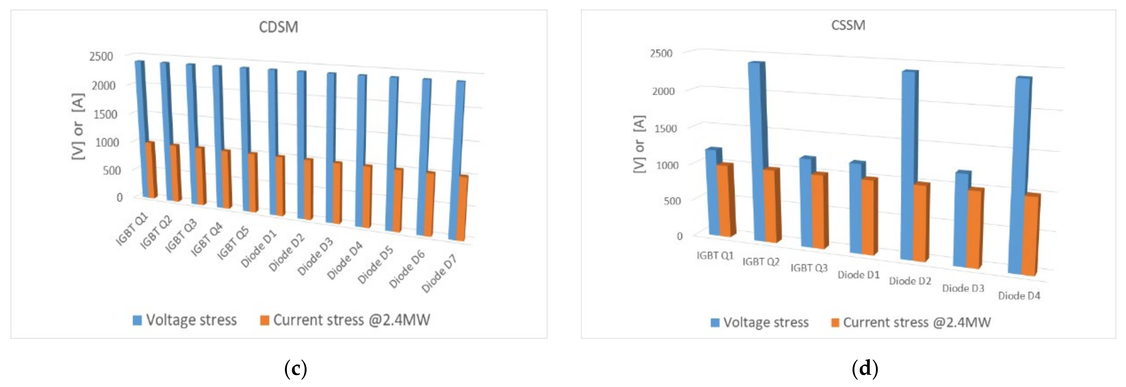
3.3.3. Comparison of Voltage and Current Stress on the Switching Devices

Figure 11 compares the voltage and current stress applied to the switching devices according to the structure of the submodule. The simple comparison of the number of parts is insufficient in economic cost analysis. Although the number of parts increases, if the voltage and current stress are low, the rated values are lowered, which may be advantageous in terms of cost. Based on the submodule design parameters in Table 1, voltage and current stress are given in Figure 11. Temporary surge voltage due to switching and overcurrent due to DC short current are excluded from the analysis and are compared based on average voltage and average current.
In HBSM, FBSM, and CDSM, the voltage stress of the IGBT and diode is the same as 2400 V, and the current stress is also shown to require the same current rating at 1000 A at 2.4 MW power rating. In the case of CSSM, three IGBTs are coupled in series, and the voltage stress of the IGBTs and diodes at both ends is reduced by 50% compared to other submodules. Therefore, CSSM is advantageous in terms of cost because it is possible to use a relatively low voltage rated IGBT and a diode.

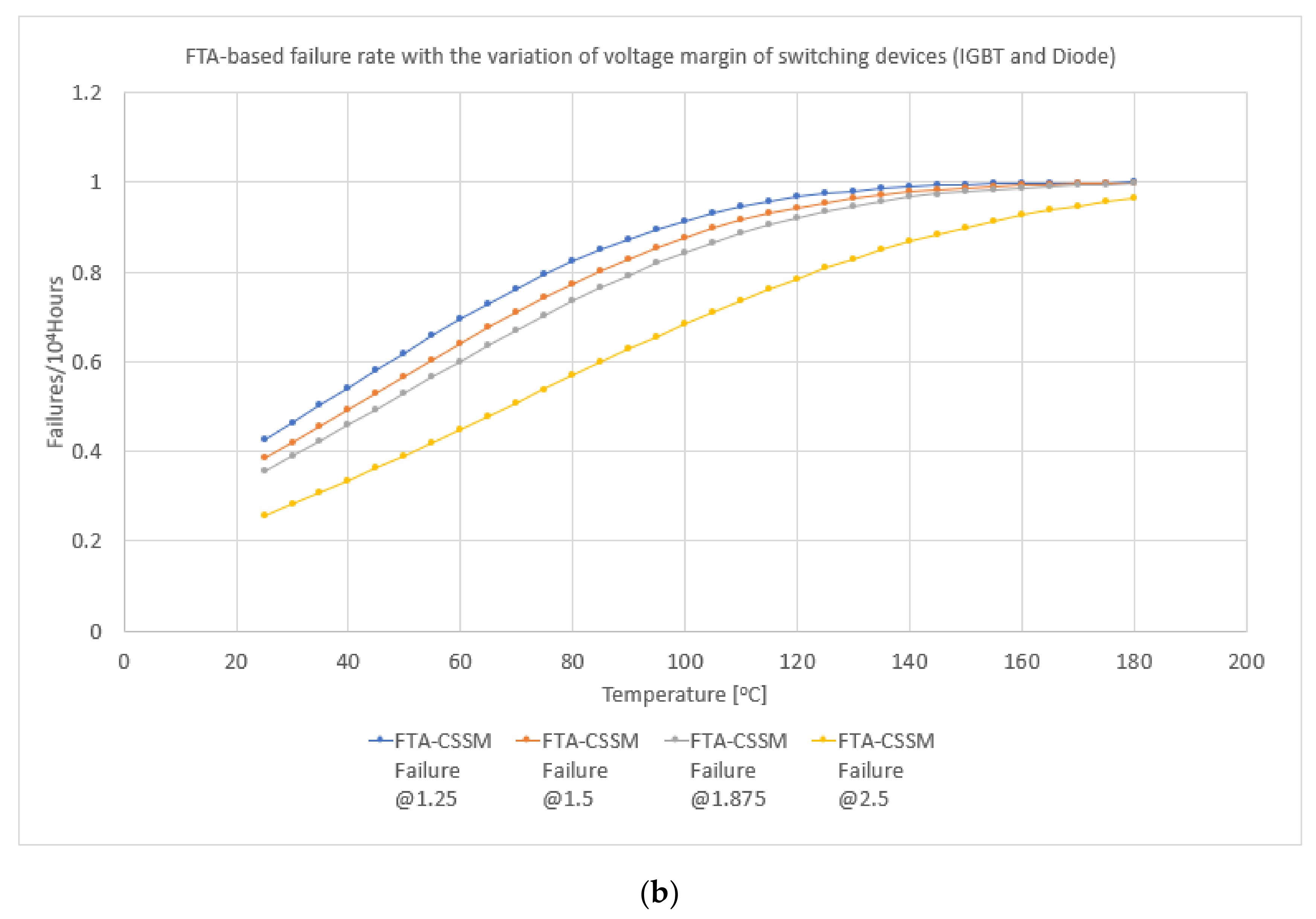
3.3.4. Comparison of Failure Rate According to Voltage Margin

The failure rate of CSSM is analyzed according to the rated voltage margin of the switching device IGBT and diode. The failure rate analyzed above is the result for switching devices (IGBT, diode) with a voltage margin of 1.875 times, so the failure rate with voltage margins of 1.25, 1.5, 2.5 times is further analyzed. Figure 12a shows the PCA results. As the voltage margin decreases, the failure rate increases proportionally. However, it is difficult to determine the proper voltage margin of the switching device as a result of PCA. Figure 11b shows the failure rate analysis result by FTA when the voltage margin of the switching device changes. It can be seen that the failure rate increases as the voltage margin decreases, but the difference between the failure rate of 1.875 times and 2.5 times decreases compared to the PCA analysis results. However, when applying IGBTs and diodes with a voltage margin of 2.5 times, it is necessary to consider cost increase and efficiency drop compared to the reduction of the failure rate.
For capacitors, the default failure rate is relatively low, so the change in the working voltage margin has a minor effect on the failure rate of the submodule. If designed to apply 1.15 times the operating voltage margin in this paper, it does not have a significant impact on reliability, and the operating voltage margin of the capacitor can be changed by further considering the average applied voltage, cost, size, and volume.

3.4. Economic Cost Analysis of CSSM and Comparison with Other Submodules

This section compares the cost according to the submodule topologies. First, we derive the cost model of each part based on the design parameters of Table 1. The cost model uses a sample of commercial parts to use the price increase ratio of the parameters that affect the price of those parts. Based on the cost model of each derived part, the prices of HBSM, FBSM, CDSM, and CSSM are compared. Each submodule consists of IGBT, diode, and capacitor, and samples of parts for the cost comparison are used by Infineon Technologies’ IGBT and diode, and TDK Electronics’ capacitor.

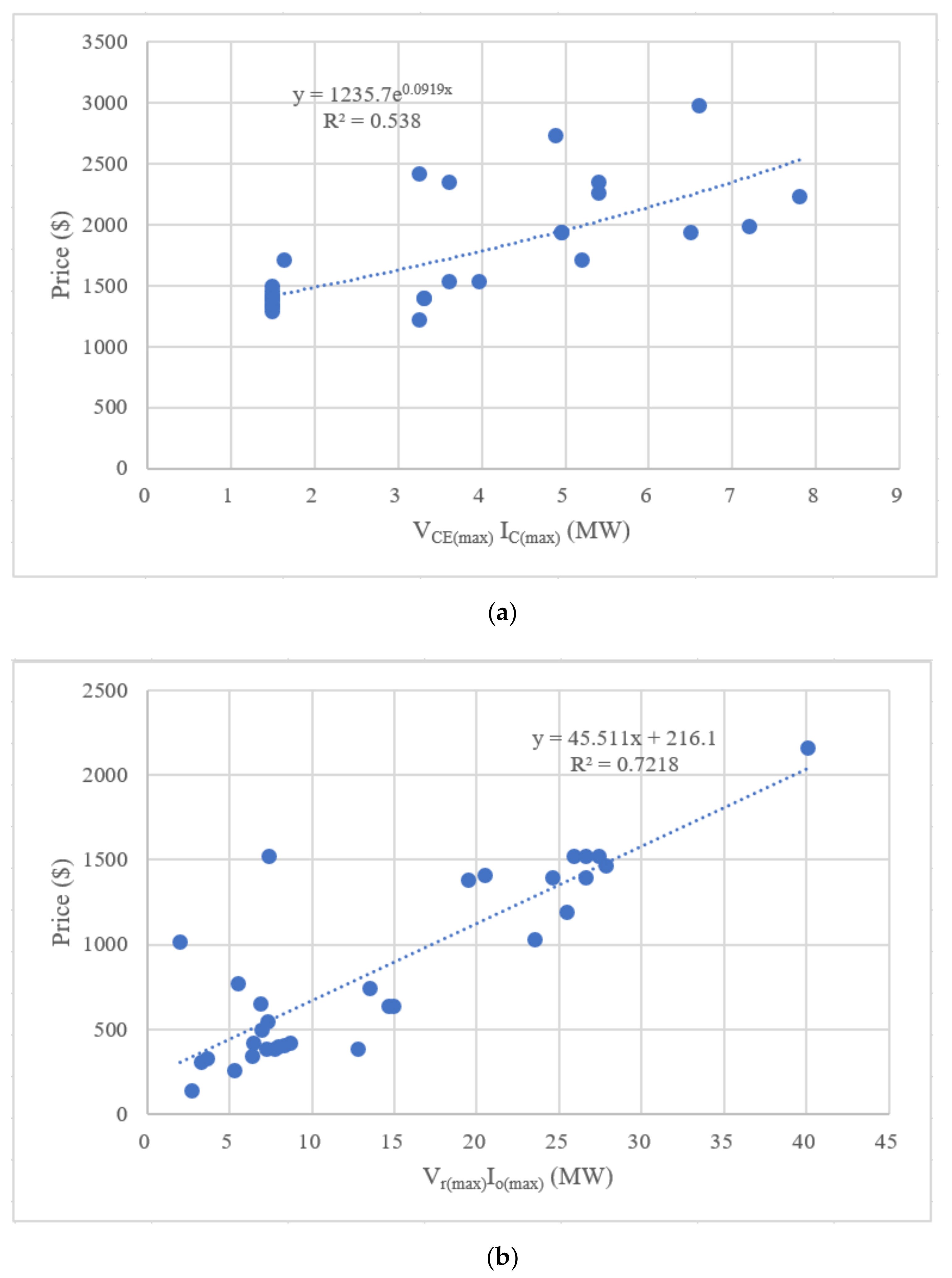
3.4.1. Cost Model of IGBT and Diode

The submodule has a voltage rating of 2400 V. Therefore, IGBT and diode use Infineon Technologies’ voltage rating of 2400 V or higher to derive the cost model. Figure 13a shows that the IGBT price varies exponentially in proportion to the values multiplied by VCE(max) and IC(max). Although the factors that affect the price of IGBT vary widely, voltage ratings and current ratings are the main factors that shape the price. Therefore, the price of IGBT is expressed as follows.
σ I G B T = 1235.7 e 0.0919 x
where x is multiplied by VCE(max) and IC(max) of IGBT, in units of MW.
Figure 13b shows that the price of diodes with a voltage rating of 2400 V or higher in Infineon technologies is linearly increasing relative to the value multiplied by Vr(max) and Io(max). The diode also has a variety of parameters that affect prices, such as IGBT, but voltage ratings and current ratings are the key factors in determining the price of diodes. The price of the diode is expressed as follows.
σ D i o d e = 45.511 x + 216.1
where x is multiplied by Vr(max) and Io(max) of the diode, in units of MW.

3.4.2. Cost Model of Capacitor

The capacitor of the submodule has a working voltage of 2400 V and a capacitance of 6900 μF. Such high-capacity high-voltage capacitors are not sold as commercial products, and customized is common. Therefore, in order to derive the cost model of the capacitor, key parameters that affect the price of the capacitor are analyzed by sampling products with a capacitance of 100 μF or more from TDK Electronics’ metalized film capacitors.
Figure 14a shows the distribution of TDK Electronics’ metalized film capacitors on the market with capacitance and voltage ratings of products with capacitance greater than 100 μF. Commercial products with the highest working voltage of the capacitor are found to have 2000 V and 1500 μF with the highest capacitance. Figure 14b shows the capacitance-dependent capacitor price, which has a significant impact on the price determination of the capacitor. The price of the capacitor is given as:
σ C a p a c i t o r = 0.0891 x + 47.809
where x is the capacitance (μF) of the capacitor.

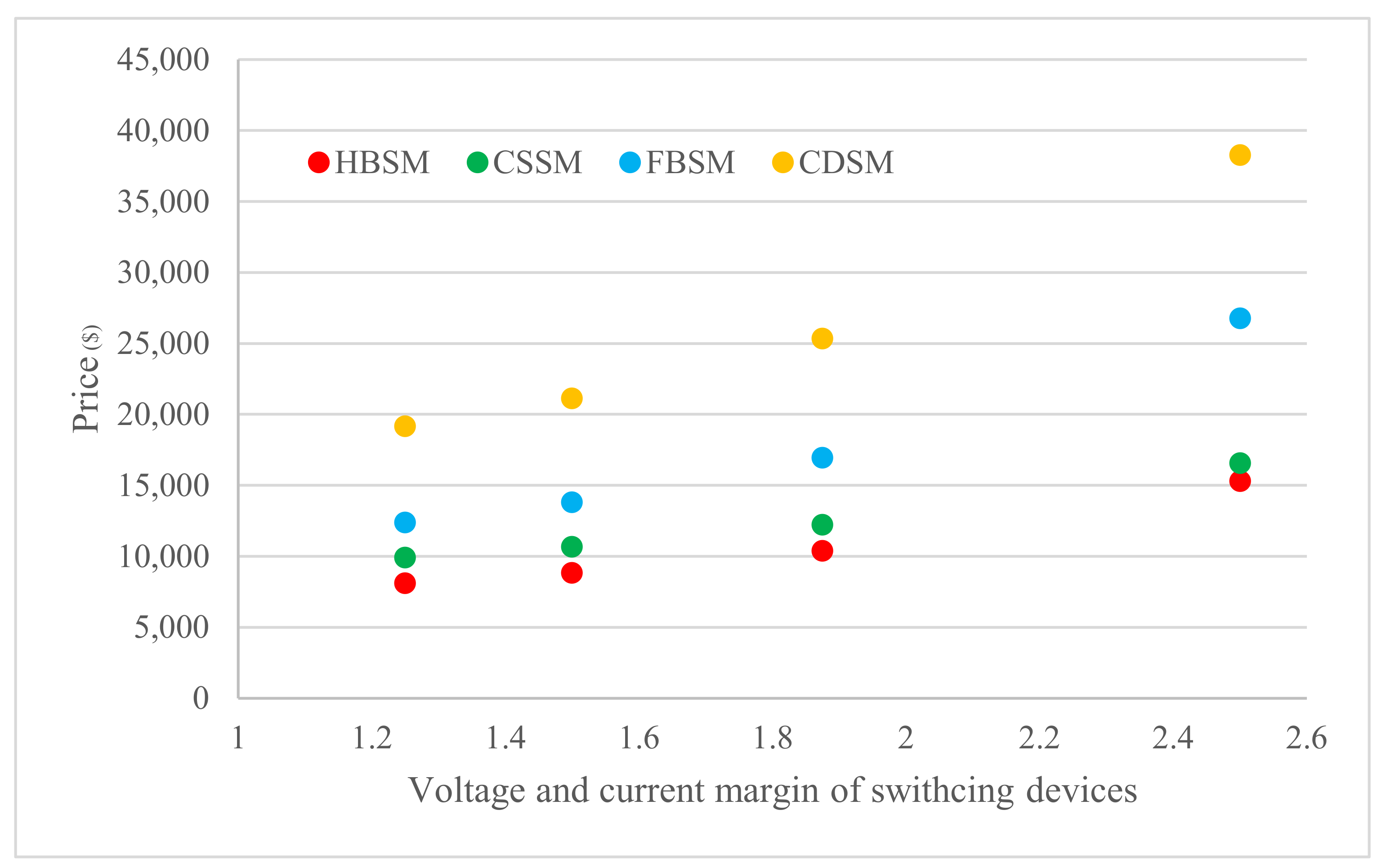
3.4.3. Cost Comparison

The failure rates analyzed in the previous sections were 1.25 times, 1.5 times, 1.875 times, and 2.5 times the voltage margin and current margin of switching devices. Thus, economic cost analysis also considers the same voltage and current rating margin. The switching devices of HBSM, FBSM, and CDSM are equal in voltage stress 2400 V and current stress 1000 A, but for CSSM, some switching devices have a voltage stress of 1200 V, which is considered in the price calculation. For capacitors, we estimate the price of a capacitor with a working voltage of 2760 V and a capacitance of 6900 μF with a voltage margin of 1.15 times. However, as shown in Figure 14a, products with a voltage rating of 2760 V and a capacitance of 6900 μF are not available on the market. Thus, the costs of producing capacitors with voltage ratings of 1320 V and capacitance of 1000 μF are estimated by connecting them in series and parallel to produce capacitors with voltage ratings of 2640 V and capacitance of 7000 μF.
Figure 15 shows the component price that consists of HBSM, FBSM, CDSM, and CSSM as the voltage and current margin increase. Although all submodules affect the price increase of submodules with increasing voltage and current margin, the CSSM shows a relatively low increase of the price thanks to the lower voltage stress of some switching devices.
Figure 16 is the result of the price comparison of submodules according to the voltage and current margin of switching devices. As the margin increases, the price of all submodules is exponentially increasing. However, it shows that the price difference between CSSM and HBSM is gradually decreasing.

4. Conclusions

In this paper, the failure rate of the clamped-single submodule (CSSM) employing DC short-circuit current protection is estimated by the FTA method. In FTA results, the failure rate is high, in the order of FBSM > CDSM > CSSM > HBSM. Adding DC short current protection improves reliability, reducing the failure rate compared to FBSM, but the failure rate is higher than HBSM due to the increased number of parts. CSSM needs an additional number of IGBTs and diodes than HBSM. However, since CSSM effectively suppresses the overvoltage and absorbs energy caused by the DC short current, it cannot be said that an increase in the number of parts decreases reliability. CSSM has three IGBTs connected in series, reducing the voltage stress of the IGBTs and diodes by 50% compared to other submodules. Therefore, CSSM is advantageous in terms of cost because low voltage rated IGBTs and diodes can be used. Finally, a comparative analysis of reliability changes taking into account voltage margins can provide guidance from various perspectives on submodule selection.

Author Contributions

Conceptualization, F.-S.K.; Data curation, Y.-G.K. and F.-S.K.; Formal analysis, F.-S.K.; Investigation, Y.-G.K., S.-G.S. and F.-S.K.; Methodology, S.-G.S.; Project administration, F.-S.K.; Resources, S.-G.S.; Software, Y.-G.K. and F.-S.K.; Supervision, F.-S.K.; Validation, Y.-G.K. and F.-S.K. All authors have read and agreed to the published version of the manuscript.

Funding

This research received no external funding.

Conflicts of Interest

The authors declare no conflict of interest.

Abbreviations and Acronyms

BJTBipolar Junction Transistor
CDSMClamped-Double Submodule
CSSMClamped-Single Submodule
FBSMFull-Bridge Submodule
FTAFault-Tree Analysis
FRDFast Recovery Diode
HBSMHalf-Bridge Submodule
HVDCHigh Voltage Direct Current
IGBTInsulated Gate Bipolar Transistor
IHSMImproved Hybrid Submodule
MOSFETMetal-Oxide-Semiconductor Field-Effect Transistor
MTBFMean Time between Failures
PCAPart Count Failure Analysis
SMSubmodule
UCVoltage Across the Capacitor of Submodule
λbThe Base Failure Rate of Part
πAApplication Factor of BJT
πCThe Contact Construction Factor of Diode
πEEnvironment Factor
πQQuality Factor
πSRThe Series Resistance Factor of Capacitor
πTTemperature Factor

References

  1. Alharbi, M.; Isik, S.; Bhattacharya, S. Reliability Comparison and Evaluation of MMC Based HVDC Systems. In Proceedings of the 2018 IEEE Electronic Power Grid (eGrid), Charleston, SC, USA, 12–14 November 2018. [Google Scholar]
  2. Xu, J.; Jing, H.; Zhao, C. Reliability Modeling of MMCs Considering Correlations of the Requisite and Redundant submodules. IEEE Trans. Power Deliv. 2018, 33, 1213–1222. [Google Scholar] [CrossRef]
  3. Guo, J.; Liang, J.; Zhang, X.; Judge, P.D.; Wang, X.; Green, T.C. Reliability Analysis of MMCs Considering Submodule Designs with Individual or Series-Operated IGBTs. IEEE Trans. Power Deliv. 2017, 32, 666–677. [Google Scholar] [CrossRef] [Green Version]
  4. Dong, Y.; Yang, H.; Li, W.; He, X. Neutral-Point-Shift-Based Active Thermal Control for a Modular Multilevel Converter under a Single-Phase-to-Ground Fault. IEEE Trans. Ind. Electron. 2019, 66, 2474–2484. [Google Scholar] [CrossRef]
  5. Xu, J.; Zhao, P.; Zhao, C. Reliability Analysis and Redundancy Configuration of MMC with Hybrid Submodule Topologies. IEEE Trans. Power Elect. 2016, 31, 2720–2729. [Google Scholar] [CrossRef]
  6. Kang, F.S.; Song, S.G. Fault-tree Analysis Based Life-cycle Expectation for Half-bridge Submodule in HVDC. Trans. Korean Inst. Elect. Eng. 2020, 69, 42–49. [Google Scholar] [CrossRef]
  7. Heo, D.H.; Kang, F.S.; Song, S.G. Failure-rate Analysis Considering Operational Condition of Half-bridge Submodule in HVDC System. In Proceedings of the 2019 International Symposium on Electrical and Electronics Engineering (ISEE), Ho Chi Minh City, Vietnam, 10–12 October 2019; pp. 252–256. [Google Scholar]
  8. Marquardt, R. Modular Multilevel Converter: A Universal Concept for HVDC-Networks and extended DC-Bus-applications. In Proceedings of the International Power Engineering Conference (IPEC), Sapporo, Japan, 21–24 June 2010. [Google Scholar]
  9. Kang, F.S.; Song, S.G. Fault-Tree Based Failure-Rate Analysis for Clamped-double Submodule employing dc-short current protecting function. J. Elect. Eng. Tech. 2021, 16, 357–365. [Google Scholar] [CrossRef]
  10. Zhang, J.; Zhao, C.; Guo, L. Simulation analysis on submodule topology of modular multilevel converter. Autom. Electr. Power Syst. 2015, 39, 106–111. [Google Scholar]
  11. Zhao, P.; Wang, C.; Xu, J.; Zong, B.; Zhao, C. A sub-module technology of MMC with DC fault ride-through capability. Power Syst. Technol. 2015, 38, 106–111. [Google Scholar]
  12. Denson, W. The history of reliability prediction. IEEE Trans. Reliab. 1998, 47, 321–328. [Google Scholar] [CrossRef]
  13. Wang, Y.D.; Song, B.F. Overview of system reliability prediction method. Aircr. Des. 2008, 28, 37–42. [Google Scholar]
  14. Li, Y.H. A brief analysis about the guide and standard of reliability prediction and estimation for electronic system and equipment. Aeronaut. Stand. Qual. 2006, 1, 50–54. [Google Scholar]
  15. Chen, S.K.; Ho, T.K.; Mao, B.H. Reliability evaluations of railway power supplies by fault-tree analysis. IET Electr. Power App. 2007, 1, 161–172. [Google Scholar] [CrossRef] [Green Version]
  16. Malhotra, M.; Trivedi, K.S. Power-Hierarchy of Dependability Model Types. IEEE Trans. Reliab. 1994, 43, 493–502. [Google Scholar] [CrossRef] [Green Version]
  17. Menis, R.; da Rin, A.; Vicenzutti, A.; Sulligoi, G. Dependable design of All Electric Ships Integrated Power System: Guidelines for system decomposition and analysis. In Proceedings of the 2012 Electrical Systems for Aircraft, Railway and Ship Propulsion, Bologna, Italy, 16–18 October 2012. [Google Scholar]
  18. Cushing, M.J.; Mortin, D.E.; Stadterman, T.J.; Malhotra, A. Comparison of Electronics-Reliability assessment approaches. IEEE Trans. Reliab. 1993, 42, 542–546. [Google Scholar] [CrossRef]
  19. Song, Y.; Wang, B. Survey on Reliability of power electronics systems. IEEE Trans. Power Elect. 2013, 28, 591–604. [Google Scholar] [CrossRef]
  20. Jones, J.; Hayes, J. A Comparison of Electronic-Reliability Prediction Models. IEEE Trans. Reliab. 1999, 48, 127–134. [Google Scholar] [CrossRef]
  21. Reliability Prediction of Electric Equipment. Department of Defense, Washington DC, Tech. Rep. MIL-HDBK-217F, December 1991. Available online: http://everyspec.com/MIL-HDBK/MIL-HDBK-0200-0299/MIL-HDBK-217F_14591 (accessed on 18 April 2021).
  22. Choudhary, K.; Sidharthan, P. Reliability Prediction of Electronic Power Conditioner (EPC) using MIL-HDBK-217 based Parts Count Method. In Proceedings of the 2015 International Conference on Computer, Communication and Control (IC4), Indore, India, 10–12 September 2015. [Google Scholar]
  23. Mou, H.; Hu, W.; Sun, Y.; Zhao, G. A comparison and case studies of electronic product reliability prediction methods based on handbooks. In Proceedings of the 2013 International Conference on Quality, Reliability, Risk, Maintenance, and Safety Engineering (QR2MSE), Chengdu, China, 15–18 July 2013; pp. 112–115. [Google Scholar]
  24. Lambilly, H.; Keser, H.O. Failure Analysis of Power Modules: A Look at the Packaging and Reliability of Large IGBT’s. IEEE Trans. Compon. Hybrids Manuf. Tech. 1993, 16, 412–417. [Google Scholar] [CrossRef]
  25. Valentine, N.; Das, D.; Pecht, M. Failure Mechanisms of Insulated Gate Bipolar Transistors (IGBTs). In NREL Photovoltaic Reliability Workshop; Center for Advanced Life Cycle Engineering (CALCE), University of Maryland: College Park, MD, USA, 2015. Available online: https://www.nrel.gov/pv/assets/pdfs/2015_pvmrw_131_das.pdf (accessed on 18 April 2021).
Figure 1. Circuit configuration of modular multilevel converter (MMC) and clamped-single sub-module: (a) 3-phase MMC; (b) CSSM.
Electronics 10 00993 g001
Figure 2. Current path of CSSM in case that submodule is connected to the converter in normal operation mode: (a) capacitor charging; (b) capacitor discharging.
Electronics 10 00993 g002
Figure 3. Current path of CSSM in the case that the submodule is disconnected to the converter in normal operation mode: (a) Q2 = ON; (b) Q3 = ON.
Electronics 10 00993 g003
Figure 4. Current path of CSSM in the case that DC short current is flowing in abnormal operation mode: (a) current is flowing into the submodule; (b) current is flowing out of the submodule.
Electronics 10 00993 g004
Figure 5. Main fault-tree of clamped-single submodule.
Electronics 10 00993 g005
Figure 6. Sub fault-tree: (a) IGBT Q1 reverse current flowing failure; (b) Capacitor charging function failure; (c) Capacitor discharging function failure; (d) IGBT Q3 reverse current flowing failure; (e) IGBT Q2 reverse current flowing failure.
Electronics 10 00993 g006aElectronics 10 00993 g006b
Figure 7. Fault dependence of the CSSM.
Electronics 10 00993 g007
Figure 8. Comparison of failure rate and MTBF by PCA and FTA: (a) failure rate; (b) mean time between failures (MTBF), year.
Electronics 10 00993 g008
Figure 9. Comparison of failure rate (a) by PCA, and (b) by FTA.
Electronics 10 00993 g009
Figure 10. Comparison of the number of circuit components for (a) IGBT and diode, (b) capacitor.
Electronics 10 00993 g010
Figure 11. Comparison of voltage and current stress on the switching devices: (a) HBSM, (b) FBSM, (c) CDSM, (d) CSSM.
Electronics 10 00993 g011aElectronics 10 00993 g011b
Figure 12. Failure rate according to voltage margin of switching devices in CSSM, (a) by PCA, (b) by FTA.
Electronics 10 00993 g012aElectronics 10 00993 g012b
Figure 13. Cost model of switching devices: (a) IGBT; (b) Diode.
Electronics 10 00993 g013
Figure 14. Price distribution and cost model of capacitor: (a) Price distribution of metalized film capacitors on the market; (b) cost model of the capacitor.
Electronics 10 00993 g014
Figure 15. Price of circuit components according to voltage and current margin: (a) HBSM; (b) FBSM; (c) CDSM; (d) CSSM.
Electronics 10 00993 g015
Figure 16. Price of submodules according to voltage and current margin of the switching devices.
Electronics 10 00993 g016
Table 1. Design parameter of CSSM.
SpecificationsValue
Rated power2.4 MW
Submodule rated voltage2400 V
Rated dc voltage2400 V
Submodule capacitance6900 µF
No. of submodules per leg108 EA
Publisher’s Note: MDPI stays neutral with regard to jurisdictional claims in published maps and institutional affiliations.

