1. Introduction
Field Programmable Gate Arrays (FPGAs) have established themselves as one of the preferred digital implementation platforms in a plethora of current industrial applications [
1]. FPGAs have evolved from a simple device for integrating glue-logic to the current complex devices, which includes more than 5 million logic cells with a host of other features such as embedded processors, DSP blocks or embedded memory blocks [
2,
3]. These characteristics make these devices ideal as reconfigurable computing platforms for real applications, allowing the mapping of complex algorithms onto hardware to achieve the demanding performance of current applications. It is usual that designers try to use FPGA resources for a different purpose than for which they were included. Following the principle called “use it or lose it”, different works in the literature have proposed an unconventional use of FPGA resources; a typical example is the use of embedded memory blocks to implement finite state machines [
4,
5,
6,
7,
8,
9,
10].
Optimizing the critical path of a circuit is essential to achieving a high performance; in many cases, this is accomplished by including special resources in FPGAs. In most datapath circuits, the critical path includes the carry chain used for arithmetic operations [
11]. In adders and subtractors, this chain generates the carry between consecutive bits. In circuits such as parity generators or comparators, the chain communicates the cumulative information needed to perform these computations [
11]. For this reason, current FPGAs provide fast routing links and special logic to perform carry operations. For example, in Xilinx FPGA devices, carry chains are composed of dedicated multiplexers and XOR gates for adding/subtracting the operands with the selected carry bits [
12].
Although carry chains are included in FPGAs to implement arithmetic circuits, they can also be used to implement some particular logic functions, such as AND or OR operations [
13,
14,
15]. In this paper, a technique for mapping arbitrary logic functions onto carry-chains is proposed. This technique includes: (1) an architecture, which is composed of blocks that implement AND or OR functions by means of Look-Up-Tables (LUTs) and carry-chain resources; and (2) a mapping algorithm to reduce the delay of the critical path and the number of used FPGA resources.
The remainder of this article is organized as follows. In
Section 2, we review the existing literature on the use of carry chains in non-arithmetic circuits. In
Section 3, a background about the use of carry chains for implementing basic logic functions is presented.
Section 4 describes the proposed architecture and algorithm in detail.
Section 5 presents the experimental results. Finally, in
Section 6, some conclusions and future works are discussed.
2. Related Works
In the literature, there are few works in which carry chains are used to improve the performance of non-arithmetic circuits. In [
16], a technique to identify logic chains in a netlist and to map them onto carry chains is presented. However, this technique cannot be applied in current FPGAs because they do not include the resources required by the proposed approach (which is only compatible with the deprecated Altera Stratix and Cyclone devices [
17,
18]). In [
19], Preusser et al. present an LUT extension based on the resources of the logic cell to propagate the carry. This extension allows the implementation of some
-input logic functions using a unique
k-LUT along with carry-chain resources; however, not all
-input functions generated by the synthesis tool can be implemented in the proposed LUT extension. In addition, the application of the proposed technique requires the use of its own cut-based approach, which does not facilitate its integration into the design flow of commercial tools. The authors claim that the combinational delay is reduced by about 20%; however, these results have been estimated using an architecture similar to Virtex-5 instead of a real device. In addition, they have been obtained without carried out the placement-and-routing. So, routing overhead is not taken into account, and therefore the performance improvement is unclear. In [
20], the proposed technique replaces the interconnection wires between logic blocks by carry chains in a post-synthesis stage. Although not all logic chains can be mapped onto carry chains, the results show that 9% of routing wires can be saved. Chu et al. [
21] propose a synthesis method that exploits carry chains for mapping general logic. The proposed technology mapping is based on majority-inverter graphs (MIGs). The MIG network is partitioned into two parts. The extracted carry-chain logic is implemented on carry chains while the rest is mapped onto LUTs as usual. The extracted carry-chain logic by the CutMap algorithm [
22] must satisfy some constraints to be mappable onto LUTs; nonetheless, final mapping shows an average delay improvement of 8% with a 10% increase in the number of LUTs. In [
23], the authors propose the use of the carry chain to implement general logic as a means of reducing the critical path delay in a post-synthesis stage. The technique selects a path in the MIG to map it onto the carry chain by estimating the potential improvement prior to LUT mapping. Once MIG nodes are selected for the carry chain, the rest of the circuit is mapped in ABC [
24] as an and-inverter graph (instead of a MIG). The results show that the technique allows to map the majority of the critical LUTs. On average, the percentage of mapped critical LUTs are 86% and 78% in area and speed optimization, respectively. This results on an average increment of the area-delay product of 9%. The main difference between this work and that presented in [
21] is that, in the former, the technique is applied before the synthesis process while in the latter it is a post technology mapping approach.
Unlike the mentioned techniques, our approach does not require a previous synthesis process because it does not work at the netlist level. Therefore, the VHDL description generated by our tool can be synthesized and implemented within the design flow of commercial FPGA tools. This is an important issue because it greatly facilitates the use of the technique by integrating it in the design flow of tools.
Another important difference is that our approach can be applied to the logic function as a whole, and not only to a determined subset of the subfunctions of which it is composed. This is possible because any logic function can be expressed as sum of minterms or product of maxterms, which only require AND and OR operations. Since the proposed technique maps these operations onto carry chains, any logic function can be implemented. By contrast, the other techniques only map the subset of subfunctions that satisfy certain constraints.
3. Background
Some basic logic functions can be implemented using carry-chains [
13,
14,
15]. Since carry chains are cascadable to form wider add/subtract logic, mapping logic functions onto carry chains is particularly interesting for implementing wide logic functions (i.e., logic functions with a large number of inputs). In the case of the AND function, it can be trivially mapped onto carry-chain resources by means of a behavioral description of an adder (see
Figure 1). This is possible because if a number is increased by one, the obtained carry bit is one only if all bits of the number are ones. This allows to exploit the carry-chain resources even when the synthesis tool does not support the mapping wide logic functions onto carry chains.
Both Xilinx and Altera/Intel provide architectural components to instantiate carry-chain resources, called primitives and Library of Parameterized Modules (LPM) functions, respectively. In Xilinx FPGA devices [
12], the carry logic is composed of dedicated 2:1 multiplexers (called MUXCYs), dedicated XOR gates for adding/subtracting the operands with the selected carry bits [
12], and dedicated connections that are independent of the general-purpose logic resources. In order to illustrate the use of these resources,
Figure 2 shows a 3-bit full adder implemented in a Xilinx device. MUXCYs can be combined with LUTs to implement basic functions, such as AND, OR, NAND or NOR operations. As an example,
Figure 3a,b shows the implementation of 24-bit AND and OR functions using carry chains, respectively. NAND and NOR functions can be implemented by changing the constant values of MUXCYs of the AND and OR implementations, respectively.
Xilinx ISE Design Suite automatically maps AND, OR, NOR or NAND functions to LUTs along with carry-chain resources when the number of inputs is large enough [
25]. This process is controlled by means of the following properties:
wide_gate_extract,
wide_gate_min_size and
wide_gate_max_size. The first property allows to enable or disable the inference of carry-chain resources for wide logic functions. The
wide_gate_min_size and
wide_gate_max_size properties specify the minimum and the maximum of the number of inputs required to apply carry-chain mapping (their default values are 36 and 500). Unfortunately, this mapping is limited to the basic functions mentioned above, and it is not supported by the current Xilinx Vivado Design Suite.
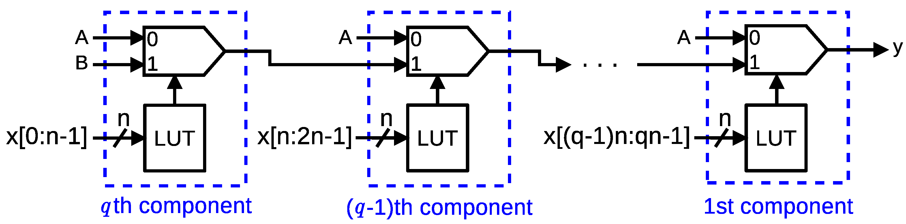
Figure 4 shows the general architecture for implementing wide logic functions using carry-chain resources (which will be referred to as CFUN). CFUN is composed of a chain of
q components, each one including one LUT and one MUXCY. The
ith component is the one located in the position
i starting with the component closest to the output of the CFUN (similarly, we will say
ith MUXCY or
ith LUT). We refer to the number of components of CFUN as its length. A CFUN of length
q allows the implementation of a logic function of up to
inputs, where
k represents the number of inputs of an LUT. Depending on the constant values
A and
B connected to MUXCYs and on the subfunction implemented in the LUTs, different logic functions can be obtained. For instance, CFUN implements the AND function if each LUT is configured as an AND,
, and
(we will refer to it as CAND). Similarly, CFUN implements the OR function if each LUT is configured as a NOR,
, and
(we will refer to it as COR).
In CFUN, the largest path between an input and the output (i.e., the critical path) is composed of the last LUT and all MUXCYs (see
Figure 4). The number of MUXCYs grows with the number of inputs of the function. However, only the last LUT is in the critical path. The delay of a MUXCY is much shorter than that of a LUT; therefore, CFUN is highly scalable. As a consequence, if the number of inputs is large enough, CFUN is faster than the conventional LUT-based implementations (i.e., those that do not use carry chains).
4. Implementation of Arbitrary Logic Functions Using Carry Chains
Let us suppose an FPGA based on k-input LUTs. An arbitrary logic function can be expressed as a product of maxterms (POM) or a sum of minterms (SOM). For POM, the proposed implementation (called CPOM) is composed of one CAND and zero or more CORs. The maxterms with less than k variables are implemented in the LUTs of the CAND while each maxterm with more than k variables is implemented using a COR whose output is connected to the CAND. Similarly, for SOM, the proposed implementation (called CSOM) is composed of one COR and zero or more CANDs that implement minterms with more than k variables. Without loss of generality, we assume that logic functions are expressed as POM in this work.
The toy example shown in
Figure 5 is used to illustrate the proposed technique (here, we consider that
k = 6).
Figure 5a shows the given logic function, which includes eight maxterms. Two of them have more than 6 variables. Therefore, two CORs are required, whose outputs are connected to LUTs of the CAND. In this way, each LUT of the CAND implements one maxterm with no more than
k variables or the product of several maxterms whenever they involve a total number of signals not greater than
k (these signals can be variables or COR outputs). Depending on the number of variables, each maxterm of the product is implemented in the own LUT or in a COR. For example, in
Figure 5b, the last LUT of the CAND (whose output is
) implements the product of the maxterms
and
; therefore, the LUT has the following input signals:
,
and
(note that the number of variables is only three even though the total number of literals is four). The first LUT of the CAND implements the product of the maxterm
and the two maxterms with more than six variables (which are implemented using CORs); therefore, the LUT has the following input signals:
,
,
,
,
, and
.
The critical path of a CPOM includes either (1) only the CAND or (2) one COR and part of (or all) the CAND, so the critical path delay is the maximum of the delays of these paths. In the first case, the path includes the last LUT of the CAND and all its MUXCYs; therefore, the delay depends directly on the length of the CAND. In
Figure 5b, the path of the CAND includes one LUT and three MUXCYs. In the second case, the delay of a path that includes a COR depends on both the length of the COR and the position of the LUT of the CAND to which it is connected. This path includes the last LUT of the COR and all its MUXCYs, the LUT of the CAND to which the COR is connected, and all MUXCYs between that LUT and the CAND output. Therefore, the path includes two LUTs. We define the depth of the COR as the sum of the length of the COR and the position
q of the LUT of the CAND to which it is connected (see the
qth elements of
Figure 4). The delay imposed by a COR depends directly on its depth. In
Figure 5b, the COR whose output is
has a depth equal to four, and its path includes two LUTs and four MUXCYs.
In a MUXCY, there exist two different kind of delays: the delay of the path between an input data signal and the output signal (which will be called data delay), and the delay of the path between the input control signal and the output signal (which will be called control delay). The critical path delay of a POM can be expressed as:
where
is the delay of a LUT;
, the data delay of a MUXCY;
, the control delay of a MUXCY;
, the length of the CAND; and
, the maximum depth of the CORs. The delay imposed by the CORs (
) can be reduced by minimizing the maximum depth of the CORs (
). This can be achieved by connecting the CORs to the CAND in decreasing order of its length starting from the first LUT of the CAND.
This paper proposes a mapping algorithm (see Algorithm 1) with the aim of reducing both the number of used resources and the delay of the critical path. The algorithm tries to reduce the number of required element by the CAND by packing more than one maxterm into each LUT, which allows to reduce the number of used LUTs and MUXCYs. This can also impact the delay when the critical path include only the CAND. In addition, the connections between the CORs and the CAND is carried out taken into account the length of the CORs in order to reduce the maximum depth of the CORs.
Without loss of generality, we assume that the logic function is expressed as a POM, thus Algorithm 1 maps functions expressed as POM to the corresponding CPOM implementation. In the case of a SOM, the corresponding mapping algorithm would be the same, but exchanging the CANDs by the CORs and replacing the AND operations by NOR operations.
Let us suppose that
k is the number of inputs of an LUT. The algorithm consists of two steps. The first one creates one COR for each maxterm with more than
k variables (see lines from two to ten). To reduce the delay of the critical path, CORs are connected to the LUTs of the CAND in decreasing order of their lengths starting from the first LUT. The second step maps the maxterms of up to
k variables onto LUTs (see lines from 11 to 21). This problem can be modelled as a Set Bin Packing (SBP) problem [
26], which is a variant of the classical Bin Packing (BP) problem [
27]. In BP, items with different sizes must be packed into bins of a fixed given capacity in a way that minimizes the number of used bins. In SBP, every item is a set, and a bin can contain items whenever the cardinality of the union of the items is less than or equal to the capacity of the bin. In our case, items represent maxterms (i.e., the set of variables of each maxterm) and LUTs represent bins whose capacity is
k. Since SBP is NP-Hard [
26], the proposed algorithm uses a greedy strategy, which is based on the First Fit Decreasing (FFD) heuristic [
27]. In this heuristic, the items are sorted in decreasing order of their sizes. For the first bin, items are packed into it following the considered order until no more items can be packed. Then, a new bin is created and the process starts with the remaining items. The procedure finishes when all items are packed. In the first iteration of the while loop of Algorithm 1,
L can contain some COR outputs not assigned to any LUT yet (i.e.,
L can be non-empty). These outputs are connected to the LUT created in the first iteration (whenever possible, along with other maxterms). The mapping algorithm reduces the number of LUTs and MUXCYs of the CAND and, therefore, the delay imposed by them. As a consequence, the algorithm can also increase the speed.
In order to illustrate the operation of Algorithm 1, we have applied it to the function shown in
Figure 5a. In the first loop, the CORs with output
and
are created and connected to the first LUT of the CAND. The algorithm packs
into the first LUT because it is the largest maxterm that can be packed into that LUT (note that only four inputs are available). Since no other maxterm can be packed in the first LUT, the algorithm executes a new iteration of the second loop. In this case, the largest maxterm is
, which is packed into the second LUT. Then,
is also packed into the second LUT although the LUT already have six inputs. Finally, the maxterms
and
are packed into the third LUT.
When functions only have maxterms with no more than
k variables, the proposed technique generates implementations composed only of one CAND. As mentioned in
Section 3, Xilinx ISE Design Suite can only map basic logic functions (AND, OR, NOR and NAND) onto carry-chains, and therefore it cannot map a POM even if it has no maxterm with more than
k variables. In these cases, the advantage of the proposed technique is that critical path only includes one LUT and the MUXCYs.
| Algorithm 1. Mapping POM to CPOM. |
Input:M is the set of maxterms, k is the number of inputs of a LUT
Output: A is the CPOM
- 1:
empty CAND - 2:
- 3:
Let be the set of maxterms whose number of variables is greater than k - 4:
for each in decreasing order of its number of variables do - 5:
Create a COR for m and add its output to L - 6:
if then - 7:
Add a LUT that implements the AND of the signals of L after the last LUT of A - 8:
- 9:
end if - 10:
end for - 11:
- 12:
whileordo - 13:
for each in decreasing order of its number of variables do - 14:
if the number of variables of is less than or equal to k then - 15:
- 16:
end if - 17:
end for - 18:
Add a LUT that implements the AND of the signals of L after the last LUT of A - 19:
- 20:
- 21:
end while
|
5. Experimental Results
The proposed technique has been evaluated with a large set of synthetic test cases, which are single-output logic functions expressed as POM. Each test case has been generated using different random values per each of the following parameters: number of variables (#Variables), number of maxterms (#Maxterms), minimum number of variables per maxterm (MinVar) and maximum number of variables per maxterm (MaxVar). The number of variables of each maxterm has been determined by a random value between the minimum and maximum assigned to the test case. The variables are negated with a probability of 50%.
Table 1 shows some statistics (the mean, the standard deviation, the minimum value, the quartiles, the maximum value) of the parameters of the test cases. AvgVar represents the average number of variables per maxterm.
We have used Xilinx Vivado Design Suite 2019.2 to synthesize and implement the test cases, so the results include the delay of the placement-and-routing stage. The target device is xc7a200tffg1156-3 (i.e., a Xilinx Artix-7 FPGA). For each test case, a VHDL structural description has been generated after applying Algorithm 1. These descriptions use Xilinx primitives to instantiate LUTs and MUXCYs; therefore, the tool does not determine the FPGA components used in the implementations (we will refer to these implementations as CARRY-MAP).
The results of CARRY-MAP have been compared to the conventional LUT-based implementations generated by Vivado (hereinafter referred to as VIV-MAP), which do not use carry chains. VIV-MAP implementations have been generated from canonical POM descriptions of the logic functions using a VHDL behavioral style. The complexity of each logic function has been measured as the number of logic levels in the critical path of the VIV-MAP. In order to provide an homogeneous sample in terms of complexity, a set of random test cases have been generated, and 30 cases have been randomly chosen for each logic level to study (from three to seven); so, a total number of 150 test cases have been used.
In order to evaluate the impact of the proposed technique in both speed and area, we have selected the following preconfigured strategies: Flow_PerfOptimized_high and Performance_ExtraTimingOpt for speed optimization in synthesis and implementation, respectively, and Flow_AreaOptimized_high and Area_ExploreWithRemap for area optimization in synthesis and implementation, respectively. The same strategies have been used for VIV-MAP and CARRY-MAP.
Regarding speed optimization,
Table 2 and
Table 3 summarize the speed increment and area reduction, respectively, obtained by CARRY-MAP respect to VIV-MAP. Both tables show the statistical measures mentioned before and the hit rate (i.e., the percentage of the cases in which the proposed technique is better). CARRY-MAP is faster than VIV-MAP in 57% of cases, but the average speed increment is zero. However, the average speed increment increases to 14% when only the success cases are taken into account. The analysis of the results by levels of logic shows that the success of the proposed technique depends largely on the complexity of the logic functions. It is observed that there is a clear increasing trend in both the speed increment and hit rate with the number of logic levels. For the cases with more than four levels, the hit rate and the average speed increment are 89% and 12% (for more than five levels, these values increase up to 97% and 17%, respectively). Regarding area results when speed optimization is used (see
Table 3), CARRY-MAP uses less number of LUTs than VIV-MAP in 72% of cases. With the exception of the functions with 3 logic levels, the hit rates are greater than or equal to 70%. In addition, the average reduction is equal to or greater than 7% for the cases with more than 4 levels. Therefore, it is important to highlight that the significant improvement of the speed is not achieved at the expense of using more resources. This is evidenced in the statistics shown in
Table 4, which relates the speed results to the area results. The hit rate represents the percentage of cases in which CARRY-MAP is better than VIV-MAP taking into account both the speed and area results; that is, the cases in which CARRY-MAP improves the speed and/or area without worsening the other parameter. Similarly, the miss rate represents the cases in which CARRY-MAP worse the speed and/or area without improving the other parameter. These results clearly show that the proposed technique is the better design option taken into account both speed and area for functions with more than 4 levels when speed optimization is used.
Table 5,
Table 6 and
Table 7 show the results for area optimization. For levels greater than 3, CARRY-MAP uses a less number of LUTs than VIV-MAP in at least 53% of cases (see
Table 5); however, the average area reduction presents positive values only for levels greater than 4. The area optimization techniques of VIV-MAP are particularly useful in complex functions with many redundant subfunctions. However, they cannot be applied to CARRY-MAP because the control signal of a MUXCY only can be connected to the output of its corresponding LUT. Nevertheless, the overall percentage of cases in which CARRY-MAP uses a lower number of LUTs is 54%, with an average reduction of 8% for these cases. Although the average area reduction is not very significant, it is achieved by improving (or without worsening) the speed results (see
Table 7, which shows that miss rate is zero or negligible for levels greater than four). In fact, CARRY-MAP improves the speed in almost all cases with more than four logical levels, reaching average increments from 8% to 26% (see
Table 6).
6. Conclusions and Future Work
In this paper, a new approach for mapping logic functions onto carry chains has been presented. Unlike other approaches, the proposed technique can be applied to any logic function. This technique includes: (1) an architecture composed of CAND and COR blocks, which include LUTs and carry-chain resources, and (2) a mapping algorithm to reduce both the delay of the critical path and the number of used FPGA resources. The algorithm uses a heuristic to interconnect COR and CAND blocks in order to reduce the delay. The problem of mapping the maxterms (or minterms) of a function to LUTs has been modelled as a SBP problem. Since SBP is NP-Hard, a greedy algorithm has been proposed, which is based on the FFD heuristic.
The results show that CARRY-MAP improves the both speed and area results of VIV-MAP for the vast majority of functions with more than 4 logic levels. These results have been obtained using both area and speed optimization. The increment of speed is, in average, more significant than that obtained for area. It is important to highlight that the improvement of one parameter (speed or area) is not achieved at the expense of the other.
As future work, we plan to study different approaches to enhance the area results. In fact, we are interested in evaluating the feasibility of a mixed architecture that uses both the proposed carry-chain mapping and conventional LUT-based synthesis depending on the complexity of the different subfunctions. We are also interested in evaluating different heuristics for the SBP. Finally, we also plan to extend the proposed algorithm to multi-output functions.


