Abstract
Logic gates made of pairs of NPN and PNP bipolar transistors, similar to CMOS logic gates, have been proposed and patented long ago but did not find any practical application until now. Other bipolar technologies (TTL, TTL-S, ECL), once the technologies of choice for digital systems, were abandoned and superseded by CMOS. In this paper it is shown that now, when truly complementary pairs of bipolar transistors can be made, properly biased bipolar gates similar to CMOS gates are feasible, can be thermally stable and find practical applications.
1. Introduction
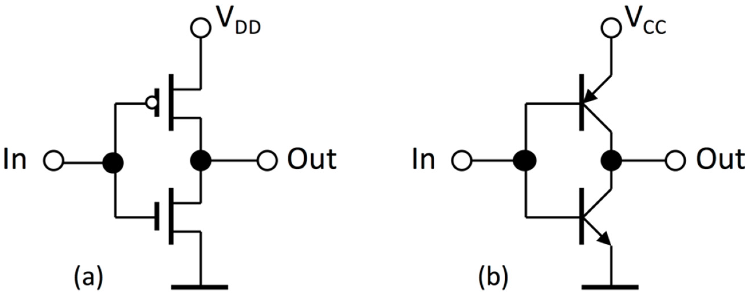
Bipolar technologies such as TTL, TTL-S and ECL, once the technologies of choice for digital systems, were totally abandoned and superseded by CMOS. The reasons are well known: large area of vertical bipolar transistors in comparison with MOS devices, larger device count in bipolar logic gates and larger power consumption. These properties made the bipolar technologies mentioned above unsuitable for VLSI circuits. CMOS-like complementary bipolar logic gates similar to CMOS logic gates (Figure 1) were proposed long ago (1976, [1]) but never used. They will be called CBip in this paper. In traditional bipolar technologies, in which TTL or ECL gates were made, good NPN vertical bipolar transistors were available but PNP transistors had different physical structures and much worse parameters. They were not complementary to their NPN counterparts. Moreover, vertical transistors were strongly asymmetric, with heavily doped emitters, much lower doping in the collector and different areas of emitter-base and collector-base junctions. Such transistors have a relatively high voltage drop between the emitter and collector when switched “on” in a digital gate. As a result, both “0” and “1” voltage levels would be degraded (“0” voltage level higher than “0” and “1” voltage level lower than the supply voltage) if asymmetric transistors were used in a CMOS-like digital gate.
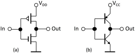
Figure 1.
Simplest logic gates: (a) inverter CMOS; (b) bipolar inverter CBip.
In 2011 a new structure of a lateral bipolar transistor on SOI, technologically compatible with PD-SOI (Partially Depleted Silicon on Insulator) CMOS circuits, has been demonstrated [2]. Such transistors are small and symmetric, complementary pairs of NPN and PNP devices can be made. Later in a series of papers [3,4,5,6,7] these transistors were investigated both theoretically and experimentally, including experimental characterization of inverters, SRAM cell flip-flops and ring oscillators. It was suggested that CMOS-like bipolar logic, i.e., logic gates made of complementary pairs of NPN and PNP transistors, could be useful both for very fast circuits and very low power circuits. Later another SOI-based technology, in which complementary pairs of symmetric NPN and PNP transistors as well as MOS devices can be made, has been demonstrated [8,9,10]. One more bipolar device concept-symmetric lateral doping-free bipolar transistor-has been proposed [11] and investigated [12,13]. In spite of these very promising works CMOS-like bipolar logic is still not used in digital integrated circuits.
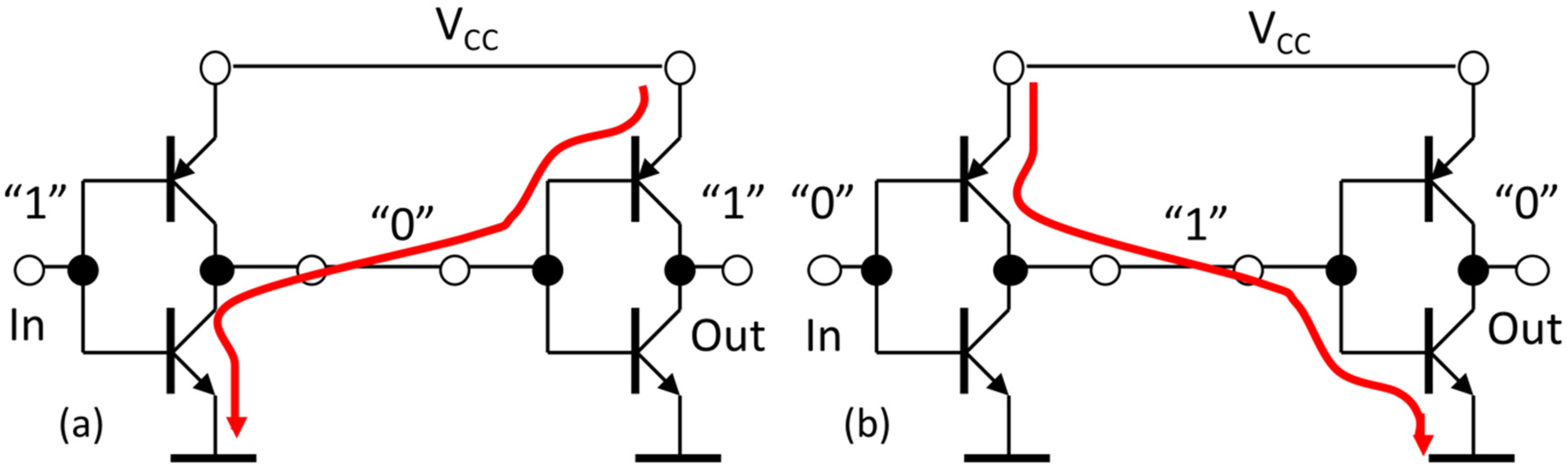
There is a fundamental difference between CMOS logic gates and similar CBip logic gates: the input current. In MOS transistors the input (gate) current is equal to zero (except gate leakage that is negligible in state-of-the-art very small devices) while in bipolar transistors the input (base) current in the “on” state is not negligible. When the output of a CBip gate is connected to the input of another CBip gate, the current drawn by this input from the output of the previous gate (as shown in Figure 2) distorts the voltage transfer curve of the previous gate.
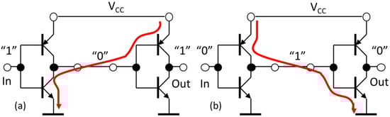
Figure 2.
Currents in a pair of CBip inverters: (a) with “1” at input; (b) with “0” at input.
The input (base) currents in CBip gates depend exponentially on the input (base-emitter) voltages and rise exponentially with temperature. This thermal effect is highly undesirable and makes CBip-based logic circuits practically useless at elevated temperatures. In this paper a simple solution mitigating this effect is proposed in Section 2, and Appendix A gives its mathematical analysis. In Section 3 CBip gates performing NOT, NOR and NAND logic functions are simulated and their properties discussed in the context of the solution proposed in Section 2. Examples of CBip-based logic circuits are also shown. Section 4 discusses the results shown in previous sections and suggests possible applications of CBip circuits. Transistor models used in simulations are given in Appendix B. These models roughly correspond to the experimental characteristics of lateral symmetric NPN devices discussed in [2] (see Figure 9 in [2]). To simplify interpretation of the simulation results, in most cases it is assumed that the models of NPN and PNP devices are identical.
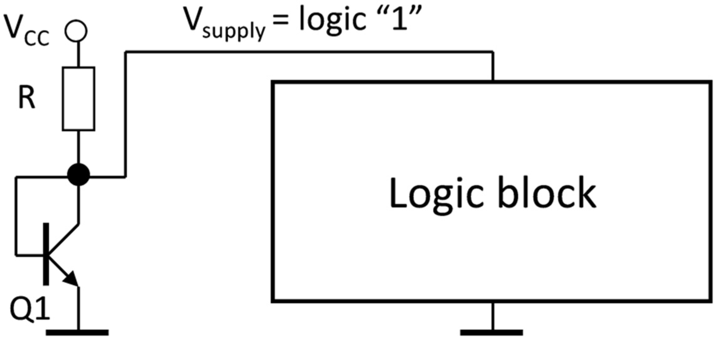
2. Thermal Stability of CBip Gates
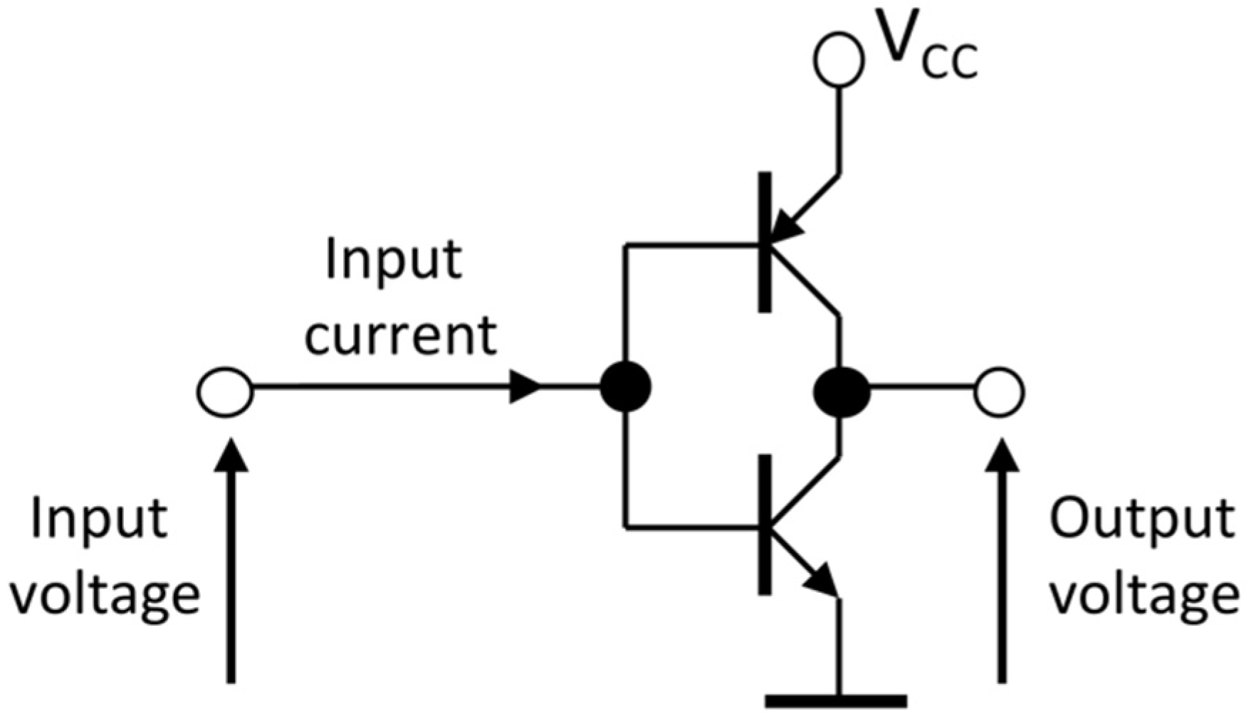
Let us consider a CBip inverter biased, as in Figure 3. It is assumed that the voltage level of logic “1” equals the supply voltage VCC.
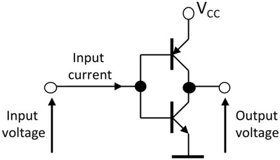
Figure 3.
Simulated CBip inverter.
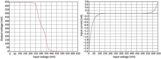
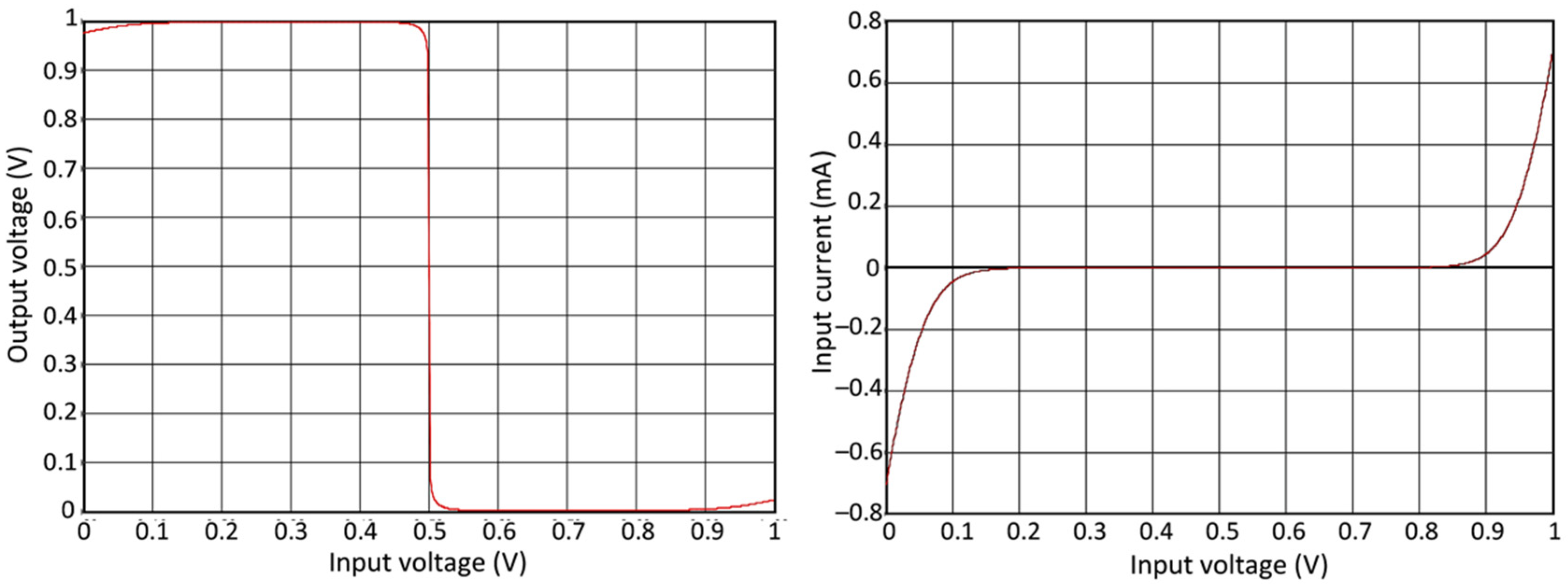
Figure 4 shows a simulated DC transfer characteristic and input current vs. input voltage for VCC = 1 V at 300 K. The transfer characteristic is excellent, but the input current is unacceptable—up to 0.7 mA.
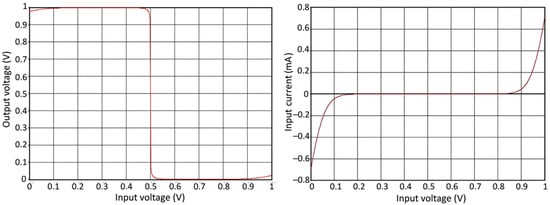
Figure 4.
Transfer characteristic and input current of a CBip inverter. VCC = 1 V, temperature 300 K.
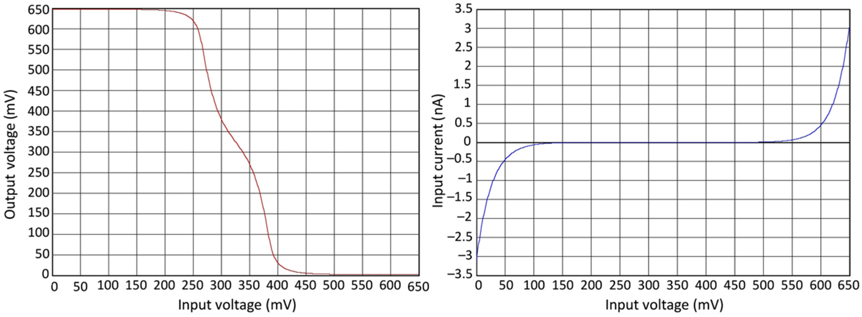
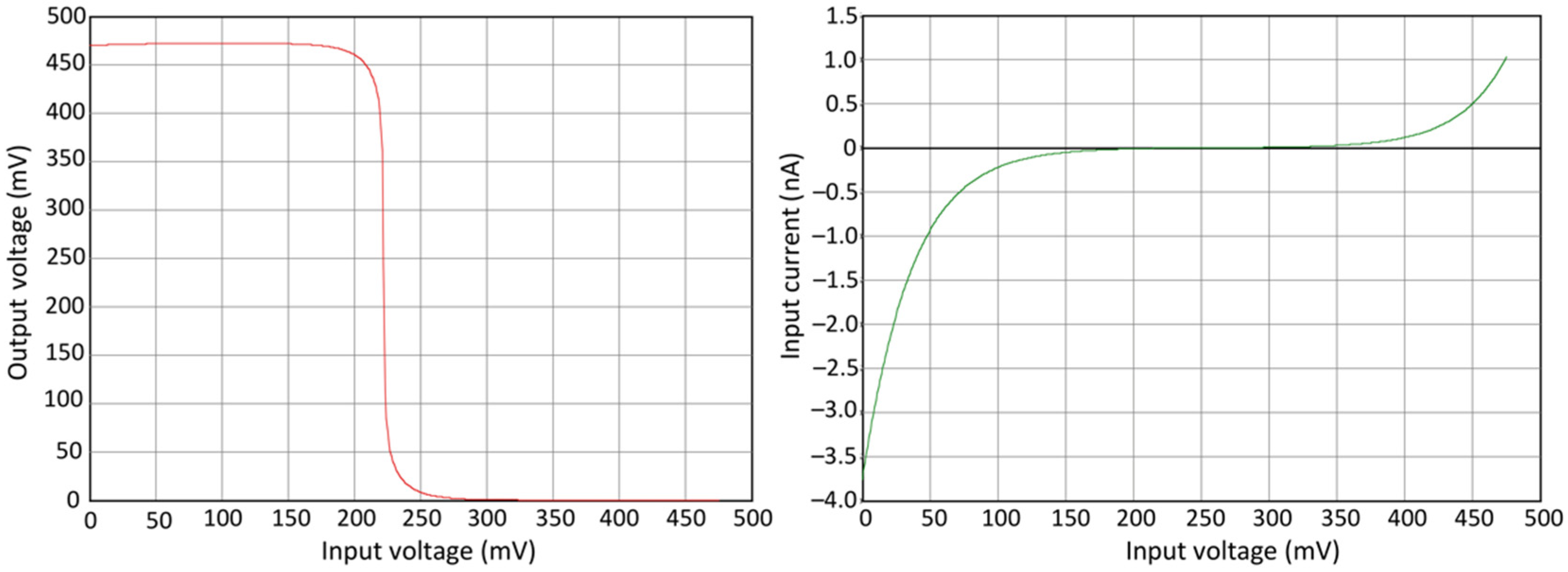
If the supply voltage is reduced to 0.65 V, the transfer characteristic is still acceptable, and the input current is reduced to nanoamperes—see Figure 5.
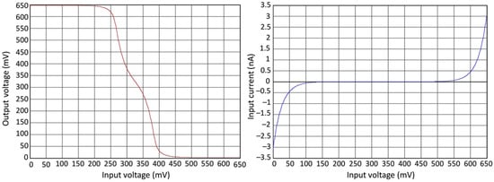
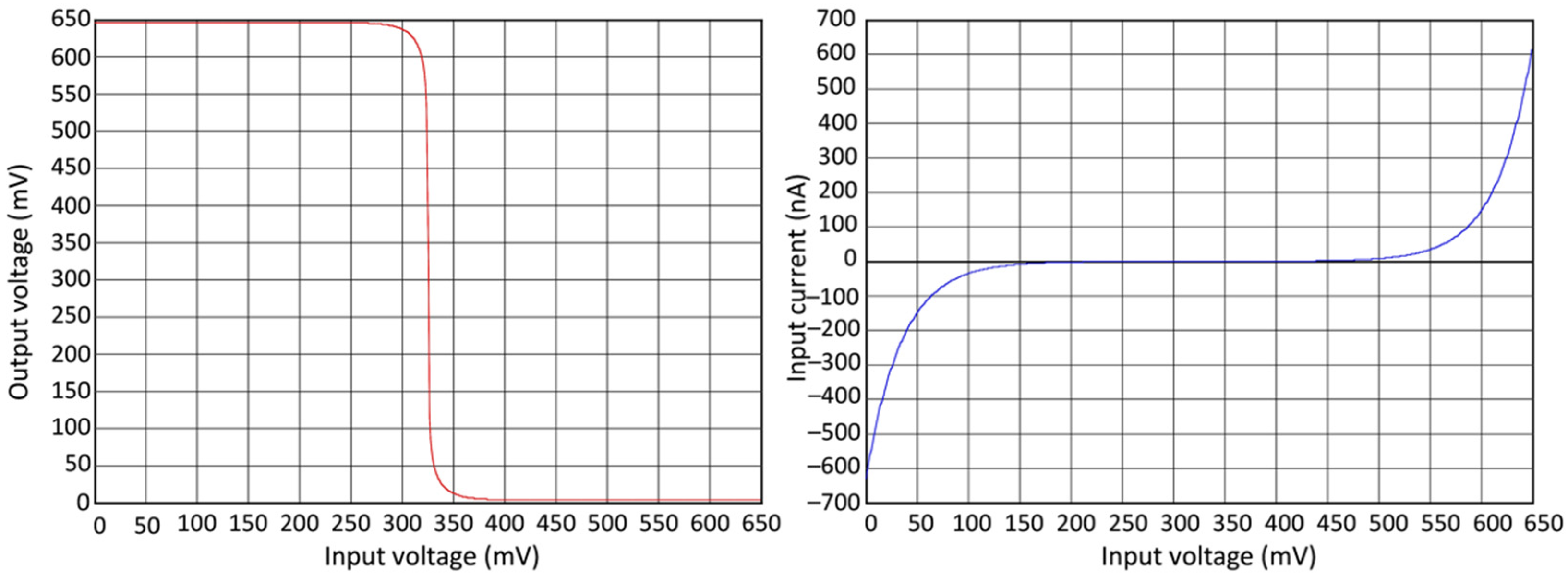
Figure 5.
Transfer characteristic and input current of a CBip inverter. VCC = 0.65 V, temperature 300 K.
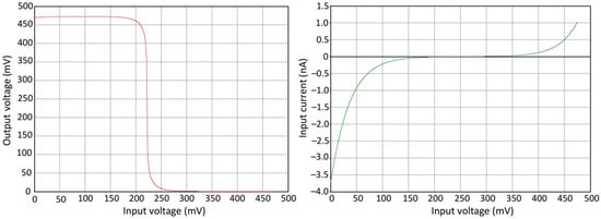
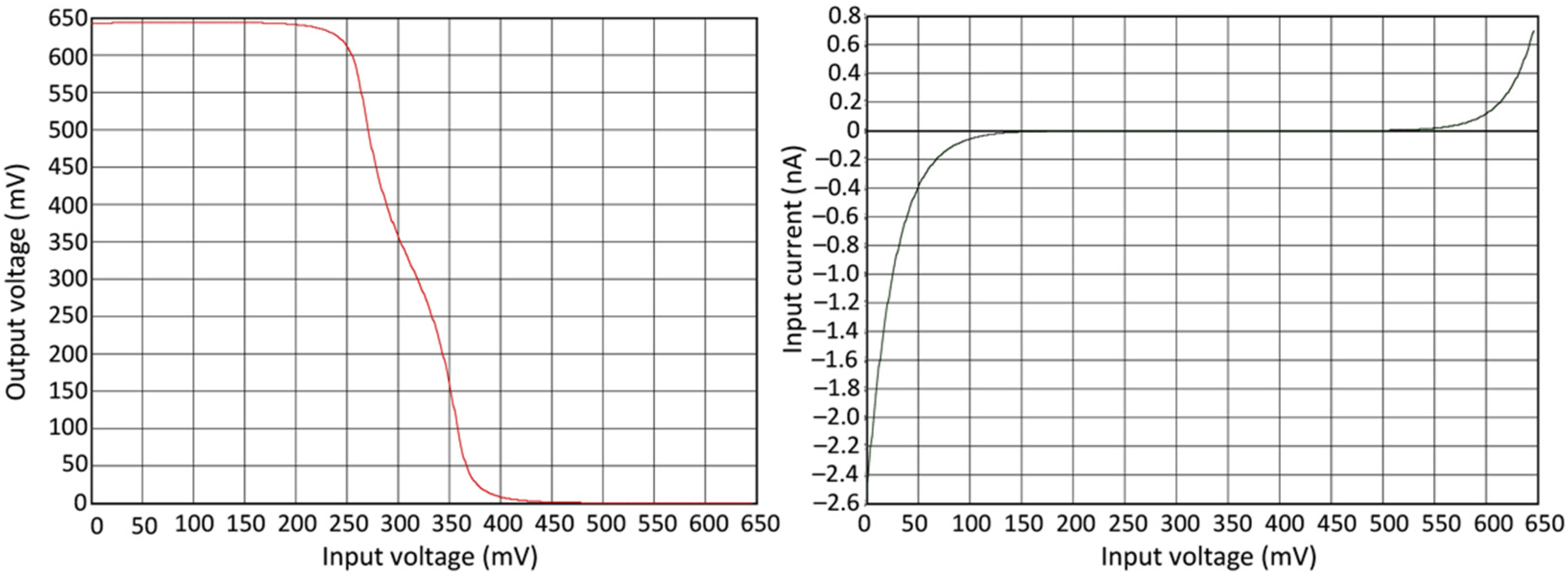
However, reduction of the supply voltage does not solve the problem of the input current because this current strongly increases with temperature. Figure 6 shows the transfer characteristic and input current at 400 K. The input current increases from 3 to 600 nA.
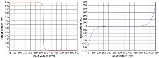
Figure 6.
Transfer characteristic and input current of a CBip inverter. VCC = 0.65 V, temperature 400 K.
To mitigate this thermal effect, a solution borrowed from an analog domain can be used. It is based on the observation that the collector current of a bipolar transistor operating in forward active mode (i.e., with VCB ≤ 0 and VBE > 0, where VCB is the collector-base voltage and VBE is the base-emitter voltage; positive voltage means forward bias and negative voltage—reverse bias of the respective transistor pn junctions) does not depend on the collector-base bias voltage (neglecting secondary effects). Therefore, if the same base-emitter voltage VBE is applied to two identical transistors operating in the same temperature, their collector currents will be identical. This directly follows from the Ebers–Moll bipolar transistor model [14]. The expression for the collector current can be written as [14] (see Equation (17) in [14]).
where IES and ICS are constants, and is the thermal voltage (approx. 26 mV at room temperature). If VCB ≤ 0, the second term can be neglected, and if VBE >> (in practice if VBE is larger than 100~150 mV), (1) can be reduced to
Expression (2) is widely used in analog bipolar circuit design.
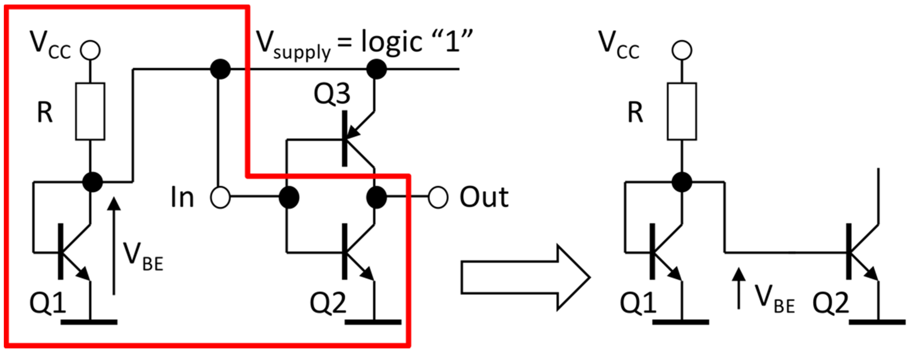
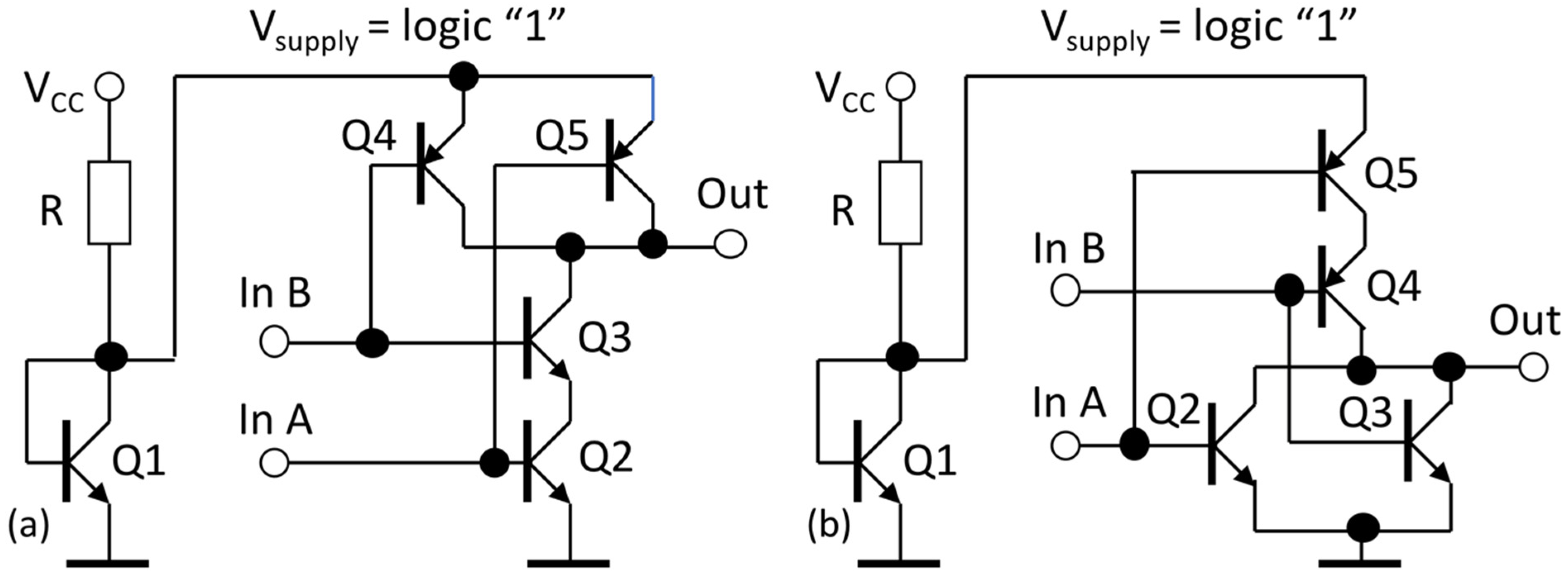
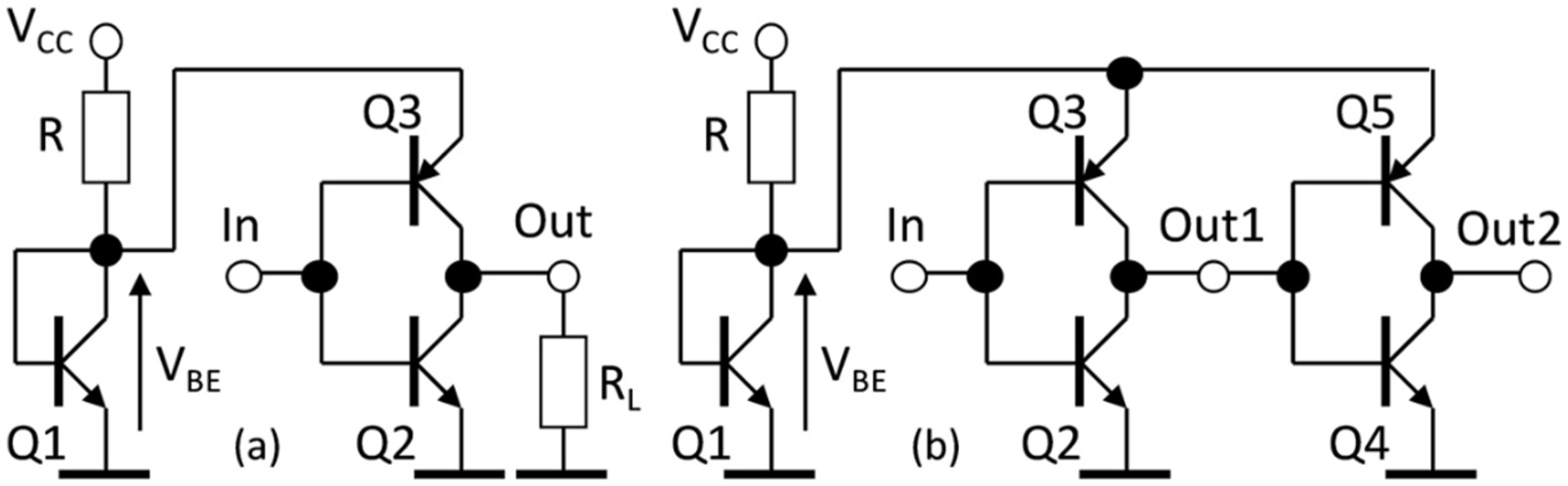
Figure 7 shows the proposed solution. The supply voltage for the CBip inverter Q2–Q3 equals the base-emitter voltage of transistor Q1. This voltage also defines the logic level “1”. With “1” (i.e., Vsupply) at the input of the inverter transistors, Q1 and Q2 make the current mirror. If both are identical and their temperatures are identical, both collector currents are the same (neglecting base currents). If the collector current of Q1 (determined by the VCC voltage and resistance R) will not depend on temperature, the collector current of Q2 also will not depend on temperature. The input current of the inverter will be hFE—times lower, where hFE is the DC current gain factor, i.e., the ratio of the collector DC current to the base DC current. The input current of the inverter will depend somewhat on temperature because hFE is temperature dependent, but this dependence is weak, not exponential. Moreover, in the configuration shown in Figure 7 the collector current of Q1 will not be absolutely constant. The current flowing across the resistor R will be equal to , and, since VBE will decrease with temperature, the current flowing across the resistor R and the collector current of Q1 will increase. In practical integrated circuits thermal dependence of the collector current of Q1 can be minimized because resistance of resistors in integrated circuits increases with temperature. Appendix A discusses this issue quantitatively. However, in this paper resistance R is constant in all simulations.
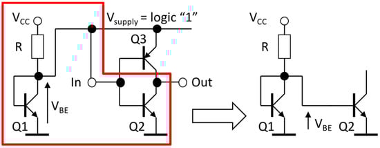
Figure 7.
The concept of thermal stabilization of CBip gates: with “1” at the input of the inverter Q1 and Q2 make the current mirror.
It is worth noting that Q1 and Q2 need not be identical. If they are not, the collector current of Q2 will be proportional to the collector current of Q1. If the collector current of Q1 does not depend on temperature, the collector current of Q2 will not depend on it either.
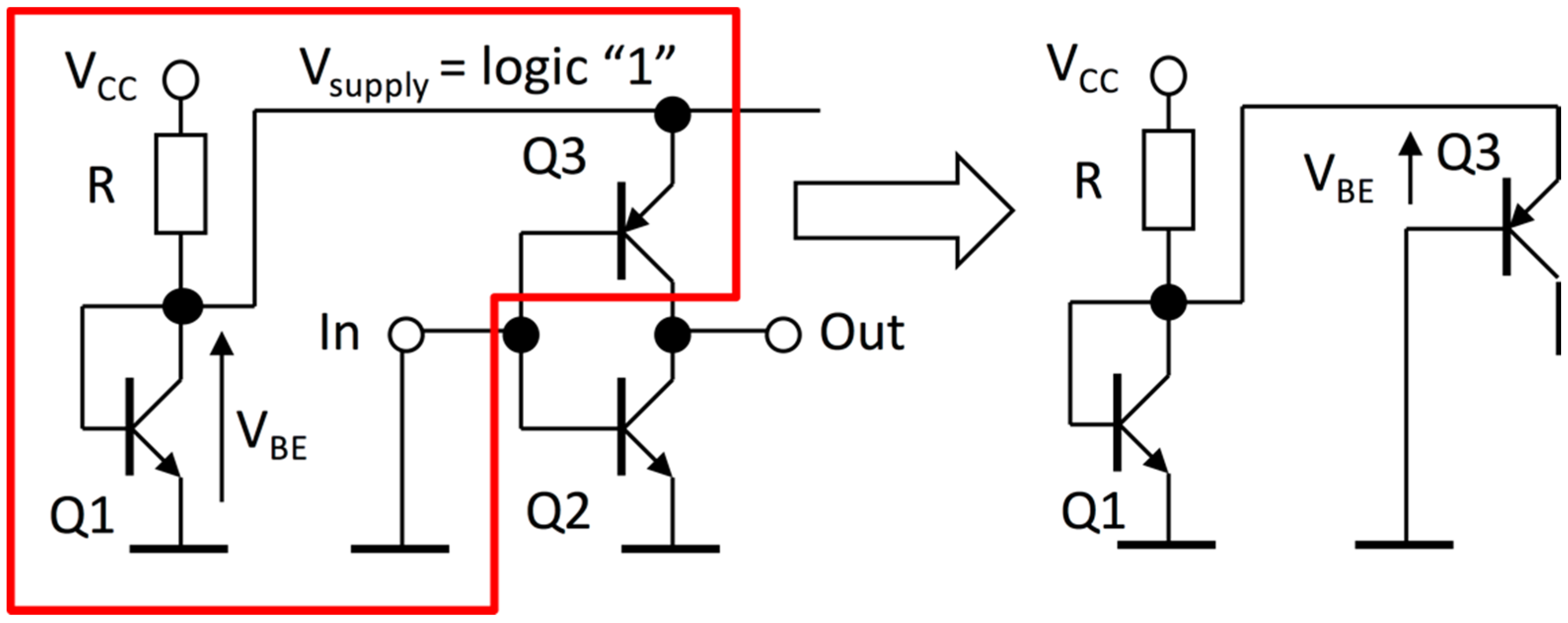
If the logic level at the input of the inverter is “0”, the current mirror is composed of transistors Q1 and Q3—see Figure 8. The base-emitter voltages of Q1 and Q3 are identical. In the general case Q1 (an NPN device) and Q3 (a PNP device) will not be identical, but since the collector current of Q1 is temperature-independent, thermal stability of the inverter will be maintained. To demonstrate this, the simulations shown in Figure 9 and Figure 10 were carried out with an NPN model different from the PNP model—see Appendix B. The input current characteristics are no longer symmetric but the input current at 400 K is almost the same as at 300 K.
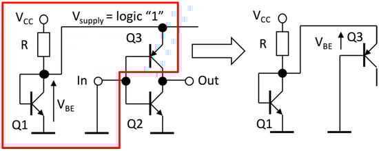
Figure 8.
The concept of thermal stabilization of CBip gates: with “0” at the input of the inverter Q1 and Q3 make the current mirror.
The thermal stabilization idea shown in Figure 7 and Figure 8 can be extended to logic blocks with any number of CBip inverters and other gates, as shown in Figure 11. By varying R, one can vary the sum of all currents consumed by the logic gates in this block, i.e., the overall current consumption. Of course, thermal stabilization of the whole block requires the same temperature of Q1 and all the transistors in the logic block.
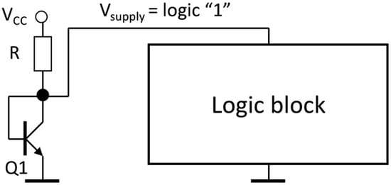
Figure 11.
Thermally stabilized logic block.
Note that an increase in the temperature from 300 to 400 K results in reduction of the supply voltage, which is also the “1” voltage level, from 650 to 465 mV (Figure 9 and Figure 10). This is not a problem in a digital circuit if the supply voltage and the “1” voltage level are the same for all CBip gates in the circuit, as in Figure 11. Examples are shown in the next section.
3. CBip Gates and Circuits
3.1. NAND and NOR Gates
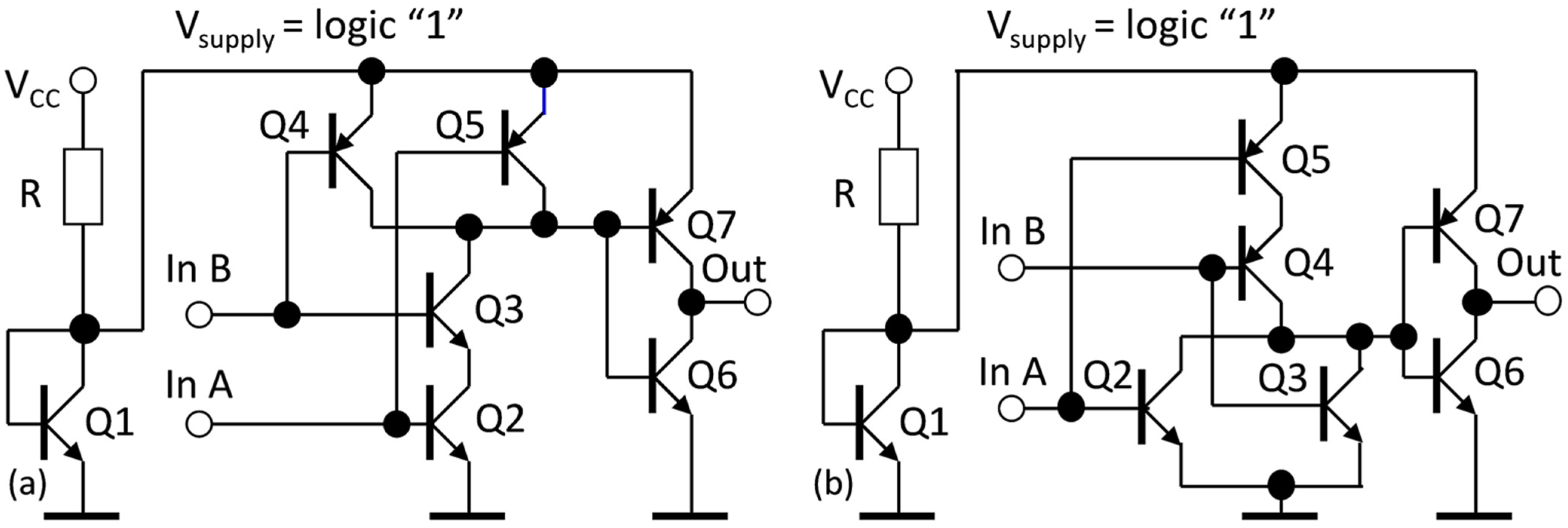
The schematic diagrams of NAND and NOR gates are shown in Figure 12.
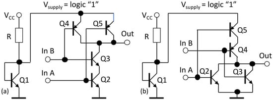
Figure 12.
Thermally stabilized CBip gates. (a) NAND gate, (b) NOR gate.
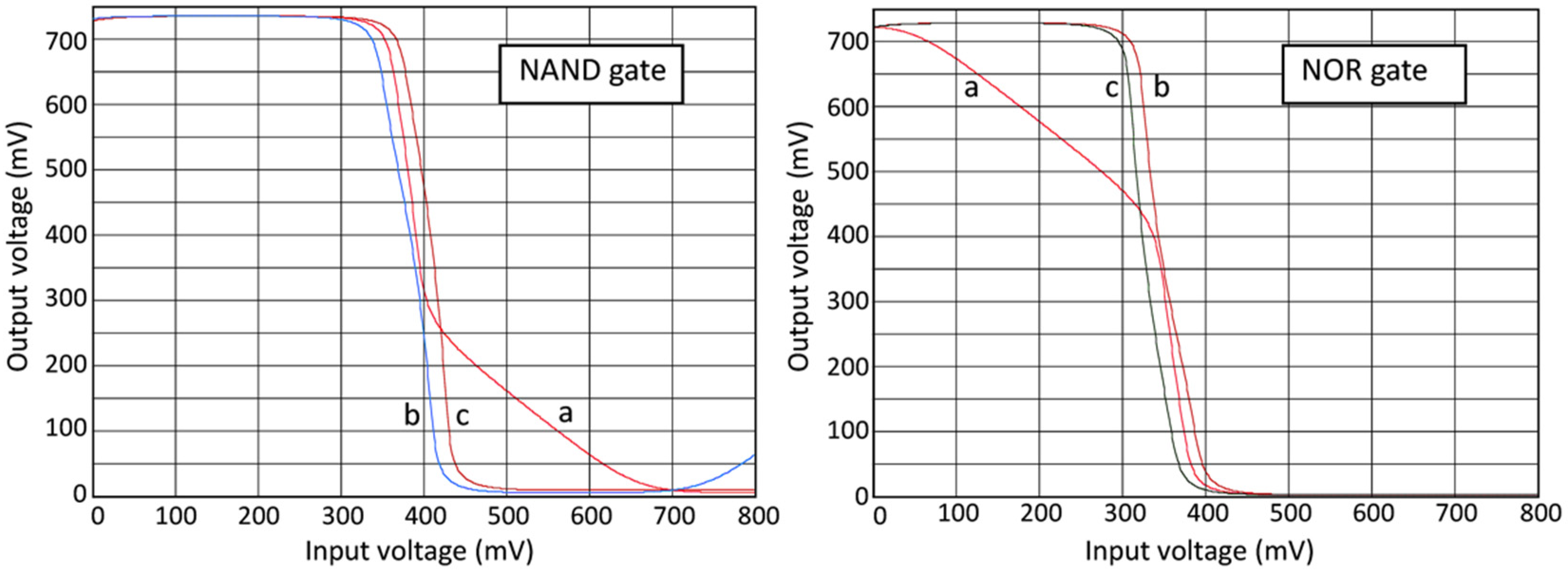
Figure 13 shows the simulated transfer characteristics of the NAND and NOR gates. Characteristics (b) and (c) are similar to the characteristics of CMOS gates. Characteristic (a) is different, somewhat similar to the transfer characteristics of the logic gates in the old NMOS technology with NMOS enhancement mode transistors as active devices and an NMOS depletion mode transistor as pull-up device. Although the (a) characteristics are not as good as (b) and (c) characteristics, the NAND and NOR gates work correctly in logic circuits, as will be demonstrated in Section 3.
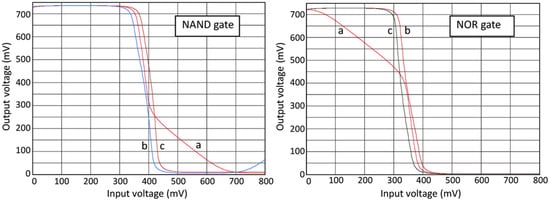
Figure 13.
Transfer characteristics of NAND and NOR gates. VCC = 1 V, R = 500 kΩ, temperature 300 K. NAND: (a) IN A: 0~800 mV, IN B: 700 mV; (b) IN A: 700 mV, IN B: 0~800 mV; (c) IN A = IN B: 0~800 mV. NOR: (a) IN A: 0~800 mV, IN B: 0; (b) IN A: 0, IN B: 0~800 mV; (c) IN A = IN B: 0~800 mV.
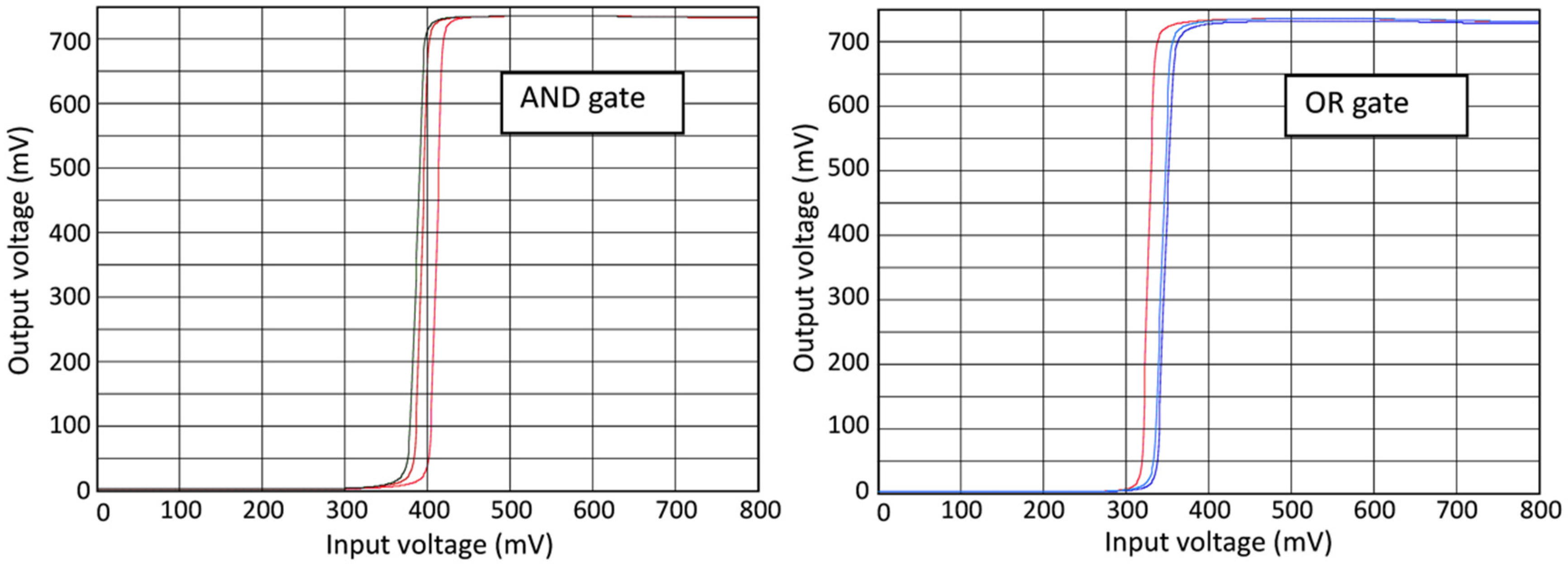
3.2. AND and OR Gates
By adding inverters at outputs of NAND and NOR gates we obtain AND and OR gates (Figure 14).

Figure 14.
Thermally stabilized CBip gates. (a) AND gate; (b) OR gate.
Figure 15 shows simulated transfer characteristics of these gates.
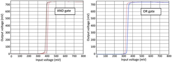
Figure 15.
Transfer characteristics of AND and OR gates. VCC = 1 V, R = 500 kΩ, temperature 300 K. AND: All three characteristics are almost the same. OR: All three characteristics are almost the same.
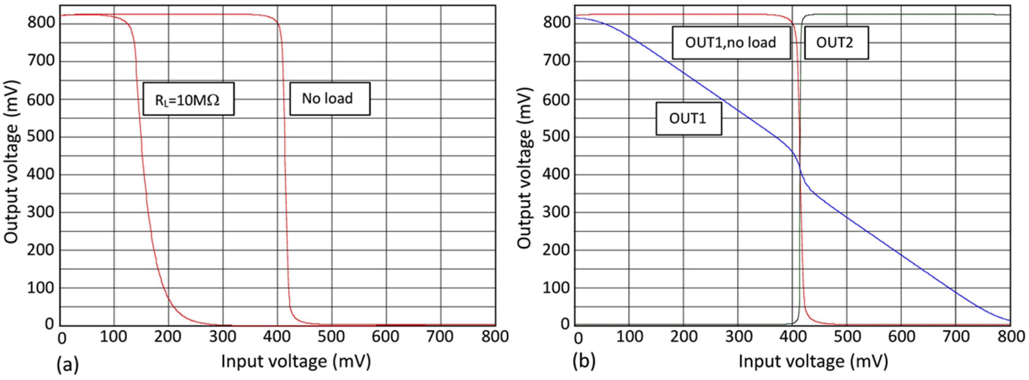
3.3. The Effects of Load
All transfer characteristics shown above (Figure 4, Figure 5, Figure 6, Figure 9, Figure 10, Figure 13 and Figure 15) were obtained for gates without any load connected to their outputs. Figure 16 shows inverters with resistive load (a) and load in the form of input of another inverter (b).

Figure 16.
Inverters with resistive load (a) and nonlinear load—input of another inverter (b).
The maximum current that can be drawn from output of any gate will never exceed the current supplied from VCC: . In practice, this means that the load resistance RL must be much larger than R. However, even resistive load that meets this requirement will shift the transfer characteristics of the gate. This is shown in Figure 17a.
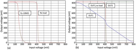
Figure 17.
Simulated transfer characteristics of inverter with resistive load (a) and inverter with nonlinear load (input of another inverter—(b)). VCC = 1 V, R = 10 kΩ, temperature 300 K.
If the output of a CBip gate is connected to the input of another CBip gate, as in Figure 16b, the transfer characteristic of the first gate is strongly distorted, as shown in Figure 17b. However, the transfer characteristic from the input to the output of the second gate is correct. In the next subsection it is demonstrated that logic blocks with CBip gates work correctly despite distortion shown in Figure 17b.
3.4. Two Examples
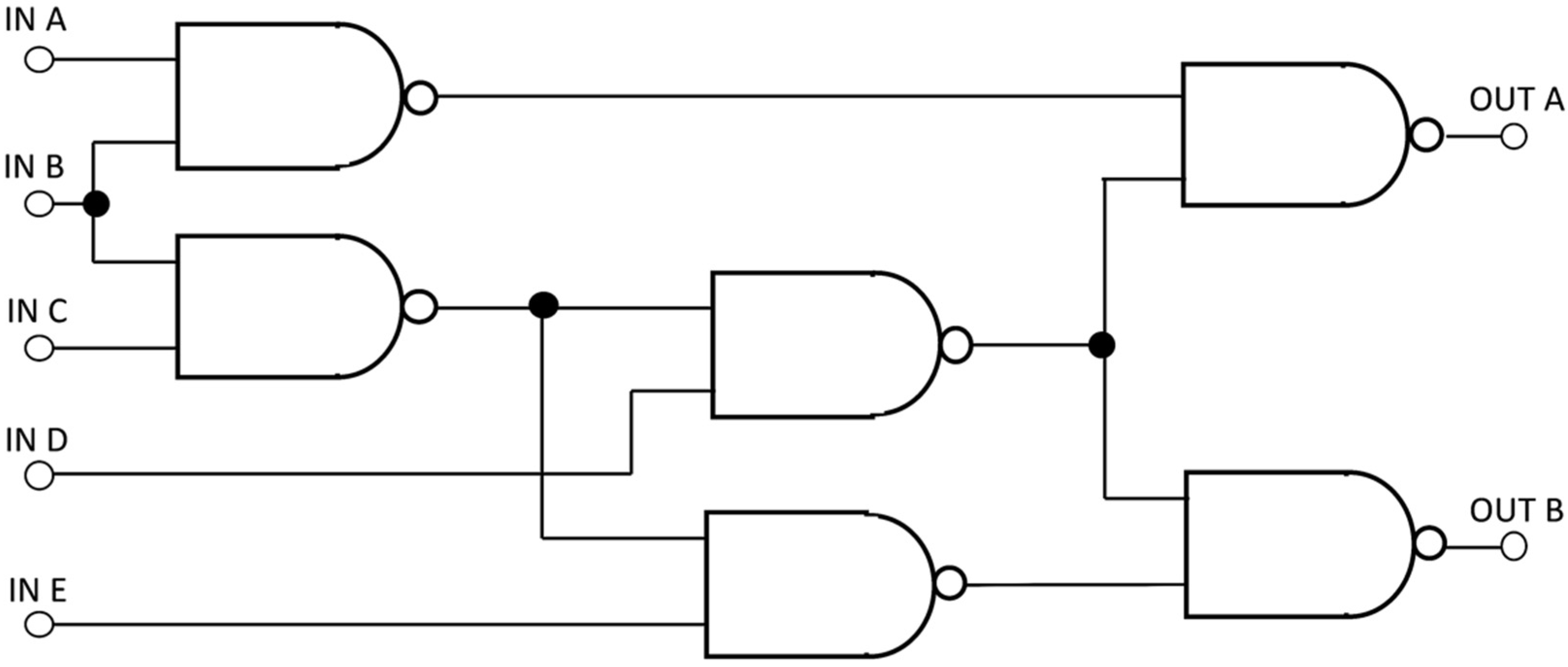
The first example demonstrates the operation of a simple logic block (C17 ISCAS benchmark) implemented with CBip gates. The logic diagram of C17 benchmark is shown in Figure 18. The block is thermally stabilized in the way shown in Figure 11.
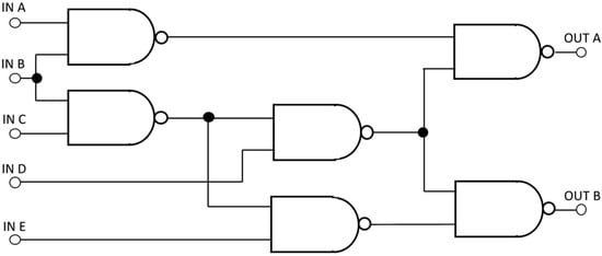
Figure 18.
The logic diagram of the C17 ISCAS benchmark.
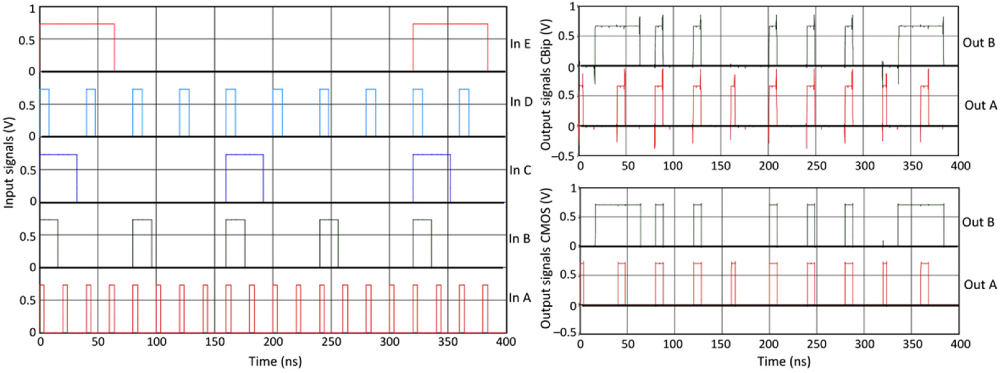
The input and output signals are shown in Figure 19. For comparison, operation of the same block implemented with 22 nm CMOS gates is shown. The logical response of the CBip-based block does not differ from response of the CMOS-based block
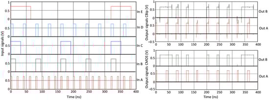
Figure 19.
Simulated operation of the ISCAS C17 benchmark: CBip and 22 nm CMOS implementation. CBip: VCC = 1 V, R = 3 MΩ. CMOS: VDD = 0.7 V. Temperature 300 K in both cases.
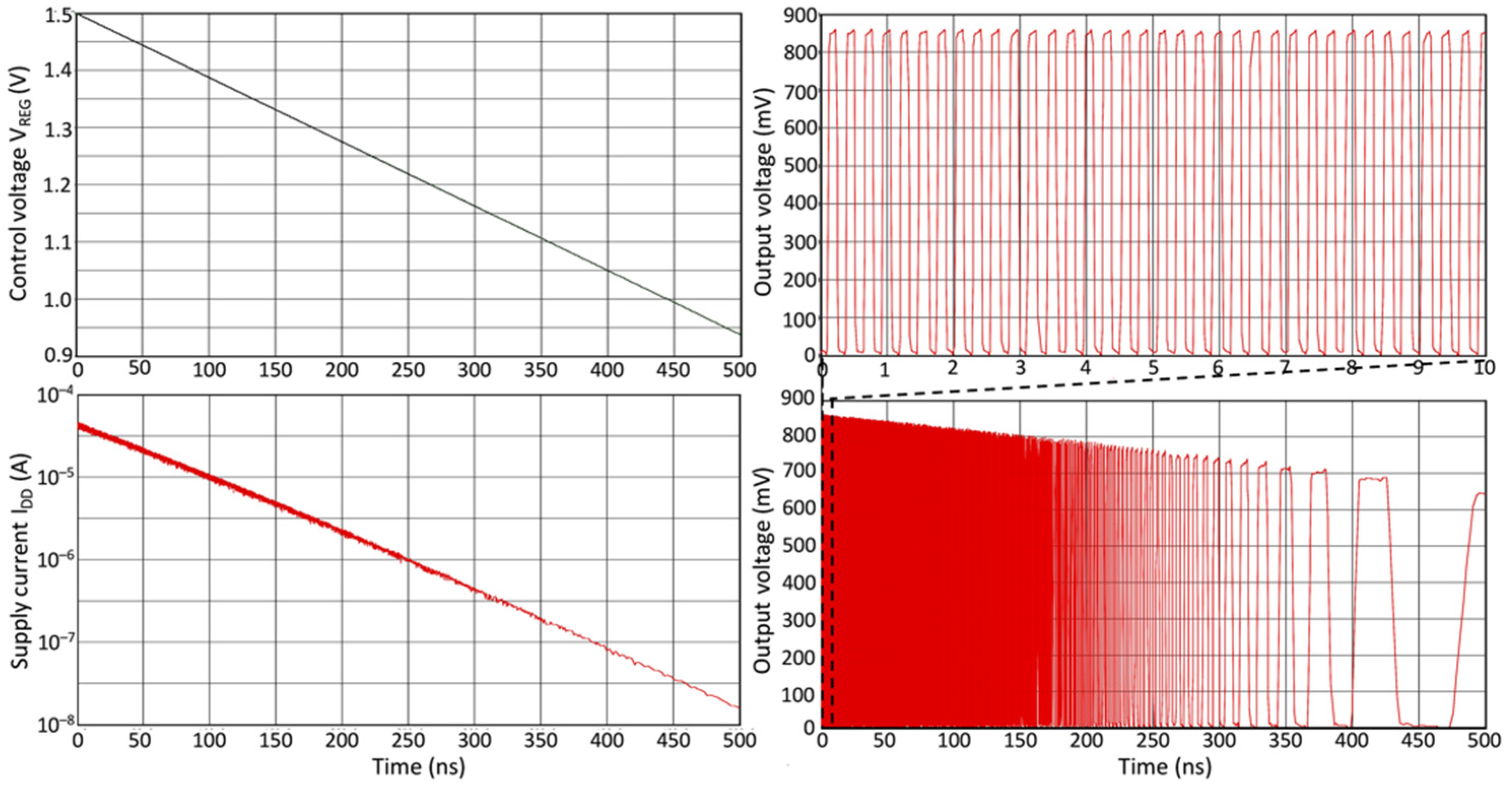
It has been demonstrated [4,6] that the delay of a CBip inverter can be varied by many orders of magnitude by varying its supply voltage. The performance of CBip-based thermally stabilized digital circuits can be adjusted by the voltage VCC and/or resistance R. The second example demonstrates this feature by replacing resistor R with a NMOS transistor, whose gate voltage is controlled by a voltage source VREG (Figure 20). By varying this voltage, the supply voltage and the frequency of oscillation of the ring oscillator are varied.
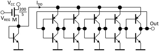
Figure 20.
Five-stage CBip ring oscillator with supply voltage controlled by a NMOS transistor M.
Figure 21 shows that the CBip ring oscillator can be used as a voltage-controlled oscillator. The shortest oscillation period at VREG = 1.5 V equals 0.28 ns; the longest period at VREG = 0.95 V is approximately 125 ns. This simulation demonstrates the flexibility of CBip-based logic circuits: the same circuit can be used either as a high-performance circuit or as a low-power circuit by changing the VCC voltage and/or the resistance R (Figure 7 and Figure 8). If the resistance R is replaced by an active voltage-controlled device, as in Figure 20, the performance and power consumption can be easily controlled in a working circuit and adjusted as needed for a given task.

Figure 21.
Simulated operation of five-stage CBip ring oscillator with supply voltage controlled by a NMOS transistor: control voltage, supply current (log scale) and output voltage as a function of time; VCC = 1.2 V, temperature 300 K.
For comparison, Figure 22 shows the same CBip ring oscillator simulated at temperature 400 K. The IDD current is larger and oscillator periods are shorter. The shortest oscillation period at VREG = 1.5 V equals 0.19 ns; the longest period at VREG = 0.95 V is approximately 5 ns only. This simulation result is also affected by temperature dependence of the parameters of the MOS transistor M and capacitances of bipolar devices.
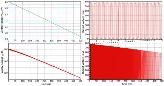
Figure 22.
Simulated operation of five-stage CBip ring oscillator with supply voltage controlled by a NMOS transistor: control voltage, supply current (log scale) and output voltage as a function of time; VCC = 1.2 V, temperature 400 K.
4. Discussion and Conclusions
The purpose of this paper is to show that CBip gates thermally stabilized as shown in Figure 7 and Figure 8 can be used to build fully functional digital circuits working well in a broad range of temperatures. A unique feature of CBip-based digital circuits is that the same circuit can be used either as an ultra-low power circuit or as a high-performance circuit, and power vs. performance tradeoff can be easily controlled in a working circuit.
But the question is: who needs CBip gates?
It is rather obvious that CBip-based digital circuits will not replace the most advanced FinFet or Nanosheet-based CMOS circuits. However, they can become a valuable addition to more traditional CMOS circuits. The symmetric lateral bipolar transistors on PD-SOI substrates [2,3,4,5,6,7] and CBip gates using them could be used as additional components of PD-SOI CMOS circuits, for example in I/O buffers, or even as either high-performance or ultra-low power digital blocks, as suggested in [5,6,7]. The doping-free symmetric lateral bipolar transistors [11,12,13] could be added to FD-SOI (Fully Depleted Silicon on Insulator) CMOS circuits, where the channel area of MOS devices is not intentionally doped. Unfortunately, manufacturers do not offer symmetrical lateral bipolar transistors in their PD-SOI or FD-SOI technologies yet. Therefore, the simulations described in the paper cannot be directly compared with experiments. However, the transistor models used in the simulations roughly correspond to the experimental characteristics of NPN devices discussed in [2] (Figure 9).
It is worth noting that bipolar transistors are very useful in analog circuits. In mixed-signal circuits the symmetric lateral bipolar transistors could be used, e.g., in low-noise amplifiers as well as in RF amplifiers. This topic is, however, beyond the scope of this paper.
Funding
This research was funded by Narodowe Centrum Badań i Rozwoju, grant number PBS1/A3/4/2012.
Conflicts of Interest
The author declares no conflict of interest.
Acronyms
For convenience of the readers acronyms used in the paper are listed below.
| NPN | denotes bipolar transistor with emitter and collector made of n-type semiconductor and base of p-type semiconductor. |
| PNP | denotes bipolar transistor with emitter and collector made of p-type semiconductor and base of n-type semiconductor. |
| CMOS | Complementary Metal-Oxide-Semiconductor—logic gates that use complementary pairs of p-type and n-type MOS transistors. |
| TTL | Transistor–Transistor Logic—logic gates that use NPN bipolar transistors. |
| TTL-S | Transistor—Transistor Logic with Schottky diodes—logic gates that use NPN bipolar transistors with Schottky diodes in order to reduce the switching time of bipolar transistors. |
| ECL | Emitter-Coupled Logic: another kind of logic gates that uses bipolar transistors. |
| VLSI | Very Large-Scale Integration—technology enabling fabrication of complex integrated circuits, which combine millions of MOS transistors in a single semiconductor chip. |
| SOI | Silicon on Insulator—silicon layer located on top of silicon dioxide insulating layer. |
| SRAM | Static Random-Access Memory—semiconductor memory that preserves the content of memory cells as long as they are powered, no refreshing of the content necessary. |
| PD-SOI | Partially Depleted Silicon on Insulator—CMOS technology in which MOS devices are made in a relatively thick silicon layer located on top of silicon dioxide insulating layer. |
| FD-SOI | Fully Depleted Silicon on Insulator—CMOS technology in which MOS devices are made in a very thin silicon layer located on top of silicon dioxide insulating layer. |
| CBip | Logic gates discussed in this paper that use complementary pairs of bipolar NPN and PNP transistors, different from TTL, TTL-S or ECL gates. |
| NAND, NOR, AND, OR | Names of logic gates performing the respective logic functions. |
| RF | Radio Frequency—name often used for electronic circuits working in the microwave range of frequencies. |
Appendix A. Analysis of Thermal Stability of a CBip Inverter
Let us consider quantitatively the thermal stability of the collector current IC of the transistor Q1 (Figure 7). At a temperature T0 this current can be calculated as follows:
The goal is to obtain constant IC, independent on temperature. The base-emitter voltage at constant collector current decreases with temperature almost linearly, typical change δVBE = 2 mV/°C. Resistance of resistors made of doped silicon increases with temperature, thermal coefficient of this resistance TCR is typically much less than 1%/°C. The collector current at a temperature T1 is
The condition for thermal stability of the collector current is
From (5) we obtain the condition for TCR:
Example: let VCC = 1.2 V, VBE (300 K) = 0.7 V (typical value), δVBE = 2 mV/°C (typical value). This gives TCR = 0.4%/°C. This estimated value corresponds to relatively low doping; doped regions in silicon ICs usually exhibit lower TCR, somewhere between 0.1%/°C and 0.3%/°C. However, this estimate shows that thermal dependence of the collector current can be minimized, even if not completely eliminated.
It is worth noting that, if the collector currents of Q1 and Q2 (Figure 7) are constant, the input current of the inverter (i.e., base current) will decrease with temperature because current gain factor hFE increases with temperature.
Appendix B. Device Models
Below device models in Berkeley Spice format, used in the simulations reported above, are listed.
- Bipolar transistor models identical for NPN and PNP devices:MODEL QMODN NPN(is = 2e-19 bf = 10 br = 10 re = 20 rb = 20 var = 25 vaf = 25 ikf = 5.15e-4
- +ikr = 5.15e-4 cje = 6e-17 cjc = 6e-17 vjc = 1 vje = 1 tf = 4.2e-12 tr = 4.2e-12)
MODEL QMODP PNP(is = 2e-19 bf = 10 br = 10 re = 20 rb = 20 var = 25 vaf = 25 ikf = 5.15e-4- +ikr = 5.15e-4 cje = 6e-17 cjc = 6e-17 vjc = 1 vje = 1 tf = 4.2e-12 tr = 4.2e-12)
- Bipolar transistor models—NPN device with higher hFE than PNP device, used in simulations shown in Figure 9, Figure 10, Figure 19 and Figure 21:MODEL QMODN NPN(is = 5e-19 bf = 100 br = 100 re = 20 rb = 20 var = 25 vaf = 25 ikf = 5.15e-4
- +ikr = 5.15e-4 cje = 2e-18 cjc = 2e-18 vjc = 1 vje = 1 tf = 4.2e-12 tr = 4.2e-12)
MODEL QMODP PNP(is = 2e-19 bf = 10 br = 10 re = 20 rb = 20 var = 25 vaf = 25 ikf = 5.15e-4- +ikr = 5.15e-4 cje = 2e-18 cjc = 2e-18 vjc = 1 vje = 1 tf = 4.2e-12 tr = 4.2e-12)
- +version = 4.6.5 binunit = 1 paramchk = 1 mobmod = 0
- +capmod = 2 igcmod = 1 igbmod = 1 geomod = 1
- +diomod = 1 rdsmod = 0 rbodymod = 1 rgatemod = 1
- +permod = 1 acnqsmod = 0 trnqsmod = 0
- +tnom = 27 toxe = 1.05e-009 toxp = 8e-010 toxm = 1.05e-009
- +dtox = 2.5e-010 epsrox = 3.9 wint = 5e-009 lint = 2e-009
- +ll = 0 wl = 0 lln = 1 wln = 1
- +lw = 0 ww = 0 lwn = 1 wwn = 1
- +lwl = 0 wwl = 0 xpart = 0 toxref = 1.05e-009
- +xl = -9e-9
- +vth0 = 0.50308 k1 = 0.4 k2 = 0 k3 = 0
- +k3b = 0 w0 = 2.5e-006 dvt0 = 1 dvt1 = 2
- +dvt2 = 0 dvt0w = 0 dvt1w = 0 dvt2w = 0
- +dsub = 0.1 minv = 0.05 voffl = 0 dvtp0 = 1e-011
- +dvtp1 = 0.1 lpe0 = 0 lpeb = 0 xj = 7.2e-009
- +ngate = 1e+023 ndep = 5.5e+018 nsd = 2e+020 phin = 0
- +cdsc = 0 cdscb = 0 cdscd = 0 cit = 0
- +voff = −0.13 nfactor = 2.3 eta0 = 0.004 etab = 0
- +vfb = -0.55 u0 = 0.04 ua = 6e-010 ub = 1.2e-018
- +uc = 0 vsat = 250000 a0 = 1 ags = 0
- +a1 = 0 a2 = 1 b0 = 0 b1 = 0
- +keta = 0.04 dwg = 0 dwb = 0 pclm = 0.02
- +pdiblc1 = 0.001 pdiblc2 = 0.001 pdiblcb = −0.005 drout = 0.5
- +pvag = 1e-020 delta = 0.01 pscbe1 = 8.14e+008 pscbe2 = 1e-007
- +fprout = 0.2 pdits = 0.01 pditsd = 0.23 pditsl = 2,300,000
- +rsh = 5 rdsw = 145 rsw = 75 rdw = 75
- +rdswmin = 0 rdwmin = 0 rswmin = 0 prwg = 0
- +prwb = 0 wr = 1 alpha0 = 0.074 alpha1 = 0.005
- +beta0 = 30 agidl = 0.0002 bgidl = 2.1e+009 cgidl = 0.0002
- +egidl = 0.8 aigbacc = 0.012 bigbacc = 0.0028 cigbacc = 0.002
- +nigbacc = 1 aigbinv = 0.014 bigbinv = 0.004 cigbinv = 0.004
- +eigbinv = 1.1 nigbinv = 3 aigc = 0.0213 bigc = 0.0025889
- +cigc = 0.002 aigsd = 0.0213 bigsd = 0.0025889 cigsd = 0.002
- +nigc = 1 poxedge = 1 pigcd = 1 ntox = 1
- +xrcrg1 = 12 xrcrg2 = 5
- +cgso = 6.5e-011 cgdo = 6.5e-011 cgbo = 2.56e-011 cgdl = 2.653e-010
- +cgsl = 2.653e-010 ckappas = 0.03 ckappad = 0.03 acde = 1
- +moin = 15 noff = 0.9 voffcv = 0.02
- +kt1 = -0.11 kt1l = 0 kt2 = 0.022 ute = −1.5
- +ua1 = 4.31e-009 ub1 = 7.61e-018 uc1 = −5.6e−011 prt = 0
- +at = 33,000
- +fnoimod = 1 tnoimod = 0
- +jss = 0.0001 jsws = 1e-011 jswgs = 1e-010 njs = 1
- +ijthsfwd = 0.01 ijthsrev = 0.001 bvs = 10 xjbvs = 1
- +jsd = 0.0001 jswd = 1e-011 jswgd = 1e-010 njd = 1
- +ijthdfwd = 0.01 ijthdrev = 0.001 bvd = 10 xjbvd = 1
- +pbs = 1 cjs = 0.0005 mjs = 0.5 pbsws = 1
- +cjsws = 5e-010 mjsws = 0.33 pbswgs = 1 cjswgs = 3e-010
- +mjswgs = 0.33 pbd = 1 cjd = 0.0005 mjd = 0.5
- +pbswd = 1 cjswd = 5e-010 mjswd = 0.33 pbswgd = 1
- +cjswgd = 5e-010 mjswgd = 0.33 tpb = 0.005 tcj = 0.001
- +tpbsw = 0.005 tcjsw = 0.001 tpbswg = 0.005 tcjswg = 0.001
- +xtis = 3 xtid = 3
- +dmcg = 0 dmci = 0 dmdg = 0 dmcgt = 0
- +dwj = 0 xgw = 0 xgl = 0
- +rshg = 0.4 gbmin = 1e-010 rbpb = 5 rbpd = 15
- +rbps = 15 rbdb = 15 rbsb = 15 ngcon = 1
References
- Berger, H.H.; Wiedmann, S.K. Complementary Transistor Circuit for Carrying out Boolean Functions. U.S. Patent 3,956,641, 11 May 1976. [Google Scholar]
- Cai, J.; Ning, T.H.; D’Emic, C.; Chan, K.K.; Haensch, W.E.; Yau, J.-B.; Park, D.-G. Complementary thin-base symmetric lateral bipolar transistor on SOI. In Proceedings of the International Electron Device Meeting, Washington, DC, USA, 5–7 December 2011; pp. 386–389. [Google Scholar] [CrossRef]
- Ning, T.H.; Cai, J. On the performance and scaling of symmetric lateral bipolar transistors on SOI. IEEE J. Electron Device Soc. 2013, 1, 21–27. [Google Scholar] [CrossRef] [Green Version]
- Cai, J.; Ning, T.H.; D’Emic, C.; Yau, J.-B.; Chan, K.K.; Yoon, J.; Jenkins, K.A.; Muralidhar, R.; Park, D.-G. SOI lateral bipolar transistor with drive current > 3 mA/µm. In Proceedings of the 2013 IEEE SOI-3D-Subthreshold Microelectronics Technology Unified Conference, Monterey, CA, USA, 7–10 October 2013; pp. 386–389. [Google Scholar] [CrossRef]
- Cai, J.; Ning, T.H.; D’Emic, C.; Yau, J.-B.; Chan, K.K.; Yoon, J.; Muralidhar, R.; Park, D.-G. On the device design and drive-current capability of SOI lateral bipolar transistors. IEEE J. Electron Device Soc. 2014, 2, 105–113. [Google Scholar] [CrossRef]
- Ning, T.H. A perspective on SOI symmetric lateral bipolar transistors for ultra-low-power systems. IEEE J. Electron Device Soc. 2016, 5, 227–235. [Google Scholar] [CrossRef]
- Ning, T.H.; Cai, J. A perspective on symmetric lateral bipolar transistors on SOI as a complementary bipolar logic technology. IEEE J. Electron Devices Soc. 2015, 1, 24–36. [Google Scholar] [CrossRef]
- Maly, W.; Singh, N.; Chen, Z.; Li, X.; Pfitzner, A.; Kasprowicz, D.; Kuzmicz, W.; Lin, Y.-W.; Marek-Sadowska, M. Twin gate, vertical slit FET (VeSFET) for highly periodic layout and 3D integration. In Proceedings of the 18th International Conference MIXDES, Gliwice, Poland, 16–18 June 2011; pp. 145–150. [Google Scholar]
- Kuzmicz, W.; Mierzwinski, P. A compact model of VES-BJT device. In Proceedings of the 20th International Conference MIXDES, Gdynia, Poland, 20–22 June 2013; pp. 96–100. [Google Scholar]
- Mierzwiński, P.; Kuzmicz, W.; Domański, K.; Tomaszewski, D.; Głuszko, G. Bipolar transistor in VESTIC technology: Prototype. Proc. SPIE 2016, 10175, 101750E-1–101750E-9. [Google Scholar] [CrossRef]
- Sahu, A.; Bramhane, L.K.; Singh, J. Symmetric lateral doping-free BJT: A novel design for mixed signal applications. IEEE Trans. Electron Dev. 2016, 7, 2684–2690. [Google Scholar] [CrossRef]
- Sahu, A.; Kumar, A.; Tiwari, S.P. Performance investigation of universal gates and ring oscillator using doping- free bipolar junction transistor. In Proceedings of the 2020 IEEE Silicon Nanoelectronics Workshop, Honolulu, HI, USA, 13–14 June 2020; pp. 125–126. [Google Scholar] [CrossRef]
- Beloni Devi, L.; Singh, K.; Srivastava, A. Study of substrate bias effect in symmetric lateral bipolar nano scale transistor on SOI for mixed signal applications. In Proceedings of the 12th IEEE International Conference on Nano/Micro Engineered and Molecular Systems, Los Angeles, CA, USA, 9–12 April 2017; pp. 673–676. [Google Scholar] [CrossRef]
- Ebers, J.; Moll, J. Large-signal behavior of junction transistors. Proc. IRE 1954, 12, 1761–1772. [Google Scholar] [CrossRef]
- Predictive Technology Models. Available online: http://ptm.asu.edu/ (accessed on 23 November 2021).


Publisher’s Note: MDPI stays neutral with regard to jurisdictional claims in published maps and institutional affiliations. |
© 2021 by the author. Licensee MDPI, Basel, Switzerland. This article is an open access article distributed under the terms and conditions of the Creative Commons Attribution (CC BY) license (https://creativecommons.org/licenses/by/4.0/).