Review

Chemical Wave Computing from Labware to Electrical Systems

by
Theodoros Panagiotis Chatzinikolaou
1,
Iosif-Angelos Fyrigos
1,
Vasileios Ntinas
1,2,
Stavros Kitsios
3,
Michail-Antisthenis Tsompanas
1,4,
Panagiotis Bousoulas
3,
Dimitris Tsoukalas
3,
Andrew Adamatzky
4 and
Georgios Ch. Sirakoulis
1,*
1
Department of Electrical and Computer Engineering, Democritus University of Thrace, 67100 Xanthi, Greece
2
Department of Electronics Engineering, Universitat Politecnica de Calatunya, 08034 Barcelona, Spain
3
School of Applied Mathematical and Physical Sciences, National Technical University of Athens, 15780 Athens, Greece
4
Unconventional Computing Laboratory, University of the West of England, Bristol BS16 1QY, UK
*
Author to whom correspondence should be addressed.
Electronics 2022, 11(11), 1683; https://doi.org/10.3390/electronics11111683
Submission received: 25 March 2022 / Revised: 4 May 2022 / Accepted: 10 May 2022 / Published: 25 May 2022
(This article belongs to the Section Circuit and Signal Processing)

Abstract

:
Unconventional and, specifically, wave computing has been repeatedly studied in laboratory based experiments by utilizing chemical systems like a thin film of Belousov–Zhabotinsky (BZ) reactions. Nonetheless, the principles demonstrated by this chemical computer were mimicked by mathematical models to enhance the understanding of these systems and enable a more detailed investigation of their capacity. As expected, the computerized counterparts of the laboratory based experiments are faster and less expensive. A further step of acceleration in wave-based computing is the development of electrical circuits that imitate the dynamics of chemical computers. A key component of the electrical circuits is the memristor which facilitates the non-linear behavior of the chemical systems. As part of this concept, the road-map of the inspiration from wave-based computing on chemical media towards the implementation of equivalent systems on oscillating memristive circuits was studied here. For illustration reasons, the most straightforward example was demonstrated, namely the approximation of Boolean gates.

1. Introduction

Chemical substrates have been successfully used to implement computations [1,2,3,4,5,6,7,8,9], thus, rendering chemical computers a significant category of unconventional computers. Although some of the examples of these unconventional computers refer to emulating basic and conventional computing procedures [10,11] (i.e., Boolean gates), recently, there has been a drive towards more interesting approaches and higher-complexity computations, like for example pattern recognition [12,13]. One of the best-established non-equilibrium systems utilized for computations is the Belousov–Zhabotinsky (BZ) reaction [14,15,16,17,18,19,20], that is mainly used as a thin layer placed on appropriate architectures (i.e., channels and reservoirs purposely designed). This reaction is characterized by colorful patterns emerging as a result of the oscillations in time and space of the concentrations of different ingredients that diffuse and react with each other. Through the aforementioned architecture of channels, the manipulation of the diffusing wave-fronts that appear in the compound is achieved, whereas their collision and annihilation are employed to perform collision-based computations [21].
The applicability of these chemical computers have been proved on a range of problems, from simple to complex. Some characteristic examples of conventional approaches are the development of a behavior similar to an electrical diode [22], gates performing Boolean logic [23,24,25], counters [26], arithmetic calculators [27,28,29,30] and associative memory [31,32]. Moreover, some more complicated implementations were tested, such as neuromorphic architectures [13,33,34,35,36,37,38], whereas the use of light as a BZ inhibitor enabled some applications of image processing [12,39,40,41,42]. Moreover, a great advantage of the chemical computers based on BZ reaction is the emerging parallelization that can be achieved by the medium. This can be confirmed by considering an elementary area of the medium as a very basic processing unit. These elementary units combine processing and memory functionality, given that they can assume one of the following three states: resting, excited and refractory. Then, the computation can be encoded as the evolution of the sum of these three states in a specific area of the system. The specific functionality of a chemical computer is achieved by the generation, diffusion, inhibition and collision of wave-fronts formulated by the oscillations of the medium through these states [43].
As the state of a chemical computer is defined by the spatial distribution of its components, resetting it can be achieved by simply stirring the compound within the reservoir. Furthermore, the diffusing wave-fronts of the components’ concentrations can be inhibited by the use of light [44,45,46] or temperature difference [47,48], whereas the initiation of these wave-fronts have been previously achieved by the immersing of silver wires within the mixture or using colloid silver [49]. For applications like Boolean logic, the diffusing wave-fronts are considered as the input and output data, when they are initiated or detected in pre-designated areas, respectively.
However, the laboratory based configurations for the chemical computers contain the disadvantage of requiring expertise on using chemistry equipment. Further disadvantages are the long time periods required for the reactants to produce output data and the sensitivity of the system to environmental conditions (i.e., temperature and vibrations). In order to alleviate these issues, the spatiotemporal simulation of the chemical reactions was proposed with mathematical tools, like the Oregonator model [47,50,51,52,53,54], Monte Carlo [55] and Cellular Automata [46,56,57,58,59,60,61,62]. Given that the approximation of results in laboratory based experiments by their simulated analogues has been proved [63,64], the simulations were extensively used as tools for better understanding of these systems and almost effortless design of more complex computing architectures.
Moreover, given that these chemical computers are expected to be better candidates for complex problems than conventional computers, they were utilized as inspiration for the development of unconventional computing circuits that would imitate their behavior and, thus, their functionality. Nonetheless, their electrical counterparts, i.e., hardware reaction-diffusion systems, will be able to accommodate more efficiently the computing capabilities described previously, as their control would be easier and the speed of executions would be higher. Nonetheless, the design of an appropriate nanoelectronic circuit that would be based on memristors would provide a tool for faster and easier conceiving of novel computing architectures. Memristors are included in the circuitry suggested along with other passive elements in order to yield the required oscillation capacity that is also observed in the chemical medium.
In detail, the proposed circuit is divided in identical building blocks, each one containing an individual and independent oscillating element. These blocks are placed in a grid-like architecture and locally interconnected with the neighboring building blocks. Each memristive building block represents a bulk area of the chemical medium, imitates the behavior of the chemical reaction-diffusion principles, and given the appropriate local interactions and spatial configuration of input voltages, the emerging functionality of the circuit can approximate the chemical computer, i.e., implementing Boolean gates. However, instead of employing diffusion of BZ compounds concentrations to encode information and execute computations, their digital counterparts are voltage waves traversing the two-dimensional grid of memristive circuitry.
Furthermore, an additional advantage of the translation of chemical computers into memristive circuits is the ability to trivially reprogram the circuit to perform multiple diverse computing operations on the same fabric. Therefore, the Turing completeness of the system may be established by the implementation of multiple Boolean gates on the same system, but, also, a further step towards implementing neuromorphic computations can be achieved.

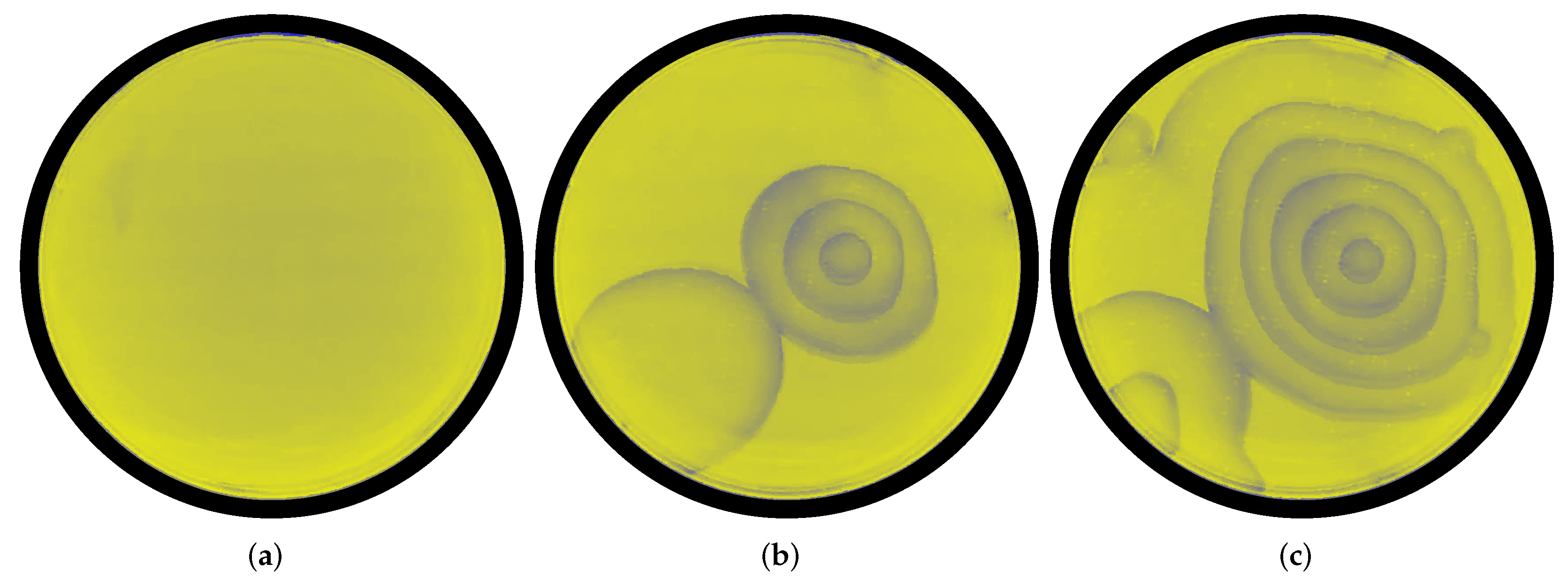
2. Chemical Wave Computing

A detailed procedure of producing BZ solution was described in [65]. Briefly, a mixture of sulfuric acid, sodium bromate, malonic acid, sodium bromide and ferroin indicator with appropriate concentrations and volumes is resulting in the final BZ solution. Then, the outcome solution was placed in a relevant container (i.e., a Petri dish or an assembly of channels that builds a Boolean gate). The mixture may become momentarily blue before reaching its equilibrium, namely yellow color (as depicted in Figure 1a). Then spontaneous excitation of chemical activity may be observed, indicated by blue waves forming (Figure 1b) and propagating throughout the container (Figure 1c). If there is no spontaneous excitation, it can be manually triggered with the use of a hot needle [65], silver wire or silver colloid [49].
One of the most straightforward applications of chemical wave computing is the implementation of Boolean gates. More specifically, one of the first paradigms of translating the wave-fronts into logic was proposed in [23]. In that study, logic gates were developed as an appropriate architecture of channels and interconnected reservoirs, for instance the proposed OR gate is depicted in Figure 2. The input channels were positioned in the left side of the architecture, while the output channels on the right. Thus, the propagation of the waves was from left to right (as illustrated in Figure 2a). The inputs of the gate were considered as True when there was an excitation of the medium in the corresponding channel (and vice versa), whereas the output of the gate was considered as True if the wave-fronts reaching the designated channels were synchronized. On the other hand, the output was considered as False, in case the wave-fronts were out of phase. Three examples of the functionality of the gate were presented in Figure 2b–d. As expected the output of an OR gate is False when all the inputs are False (except the activation input indicated as ‘1’) as illustrated in Figure 2b, where the snapshots of the wave-front from one input channel are superpositioned, and finally the output channels exhibit waves that are not synchronized. For the other two examples (all inputs set to True in Figure 2c and only one input set to True in Figure 2d), the outputs are synchronized. Thus, the resultant signal of the gate is True, as expected.
Nonetheless, more complicated gates were designed with the same “synchronization” logic principles. For instance, the combinatorial gate providing the output of AND[OR( a , b ), OR( c , d )] was proposed as depicted in Figure 3. More specifically, the input channels were located in the bottom of the gate, while the output channels on the top. Thus, the direction of the wave propagation was from bottom to top, as shown in Figure 3a. However, note that despite the different orientations of the gates, their functionality is based on the same principles. Figure 3b–d provide three examples of the combinatorial gate. As anticipated, in the example depicted in Figure 3c the gate provides a False output (waves out of phase at the output channels), as only the activation signal (‘1’) and input c are True. Moreover, in Figure 3b the activation signal (‘1’) and inputs b and d are True, resulting in True output (synchronized waves in output channels). Finally, in Figure 3d the activation signal (‘1’) and all inputs (a, b, c and d) are True, resulting in True output (synchronized waves in output channels).
Note that as previously described, the inputs were characterized by an “existence” logic, whereas the outputs by a “synchronization” logic principle. Consequently and in order to permit the cascading of multiple logic gates, the outputs should be transformed into “existence” logic. This was achieved by a special configuration of channels and a reservoir that was designed by the authors of the same study [23]. The mathematical simulation of the reaction-diffusion medium [66], whose rules govern the chemical computers, enabled a simpler and faster investigation into possible logic architectures. Thus, the design of logic gates based on the “existence” logic was proposed. Namely, the Margolus, Fredkin and Toffoli gates were designed based on simulations of the BZ with the Oregonator model [67] and later simulated with the Cellular Automata Oregonator model [62].
The equations of the Oregonator model [50], constitute a system with two variables, which can be altered to represent the photo-sensitivity of the medium [51]. The equations are as follows:
u t = 1 ϵ ( u u 2 ( f v s . + ϕ ) u q u + q ) + D u 2 u v t = u v s .
where u and v stand for the activating and the inhibiting components of the medium, respectively. Parameter q represents the speed of production for both components. Parameter f is the stoichiometry coefficient for the reactions and D u is the activating component’s diffusion coefficient. Parameter ϵ represents a time constant needed for the transmittance of one component state to the other. Parameter ϕ depicts the effects of photo-sensitivity to the medium. Namely, ϕ alters the rate of inhibitor production which is associated with the light intensity.

3. Memristive Hardware Implementation of Chemical Wave Computing

The acceleration of the computations from lab experiments to mathematical models is significant, however, further acceleration can be achieved by imitating the behavior of wave-based computers on electrical circuitry. In this work, four different circuitry configurations will be presented along with their respective applications implementing memristive circuits capable of wave propagation. Each circuit is comprised of two parts: one in charge of the wave generation and the other of propagation triggering based on the neighboring activity.

3.1. Implementing Reaction-Diffusion Dynamics on Memristor-Based LSI

Large-scale integrated circuits (LSIs) that perform semiconductor based reaction-diffusion (RD) dynamics have been proposed [2]. These LSIs, also known as RD chips, were generally influenced by Cellular Neural Networks (CNNs) or Cellular Automata (CA) rules, whereas using digital, analog, or mixed-signal complementary-metal-oxide-semiconductor (CMOS) circuits. Several CA and CNN models of RD systems [68,69,70,71,72], as well as fundamental RD Equations [73,74,75,76] were implemented using electrical cell circuits that emulate chemical reactions. In this design, each cell is placed on a two-dimensional (2-D) rectangular or hexagonal grid and coupled with nearby cells via appropriate devices that imitate 2-D spatial dissipation of chemical species and, like traditional CAs, propagate the state of the central cell to its neighbors. For example, an analog-digital hybrid RD chip [68] was developed to mirror a traditional CA simulator of BZ functionality [56].
The hardware implementation of an RD-based excitable medium [77] is discussed in the following, that includes the integration of the memristor device into the circuit. In that work memristors were utilized to model diffusion coupling in a RD-based excitable substrate. More specifically, propagating excitable waves cause a change in the conductance of the memristors, depending on their polarity. This change in conductance can control the velocity of the propagating excitable wave, with the strength of the modulation increasing as the time constant of the memristor’s model is decreasing. Patterns in the available space that are not uniform are observed and are subject to the memristor polarity, simulation and the original state of the Oregonator element. The term Oregonator element in that work is associated with an abstract circuit element that can be in one of three classes of reaction states (inactive, active and refractory) and its oscillatory cycle and excitation performance are described by a similar set of equations as the Oregonator model that was described previously.
An excitable RD model with memristors is described within the next subsections, and the spatiotemporal behaviors of 1-D and 2-D RD models are demonstrated by comprehensive numerical simulations.

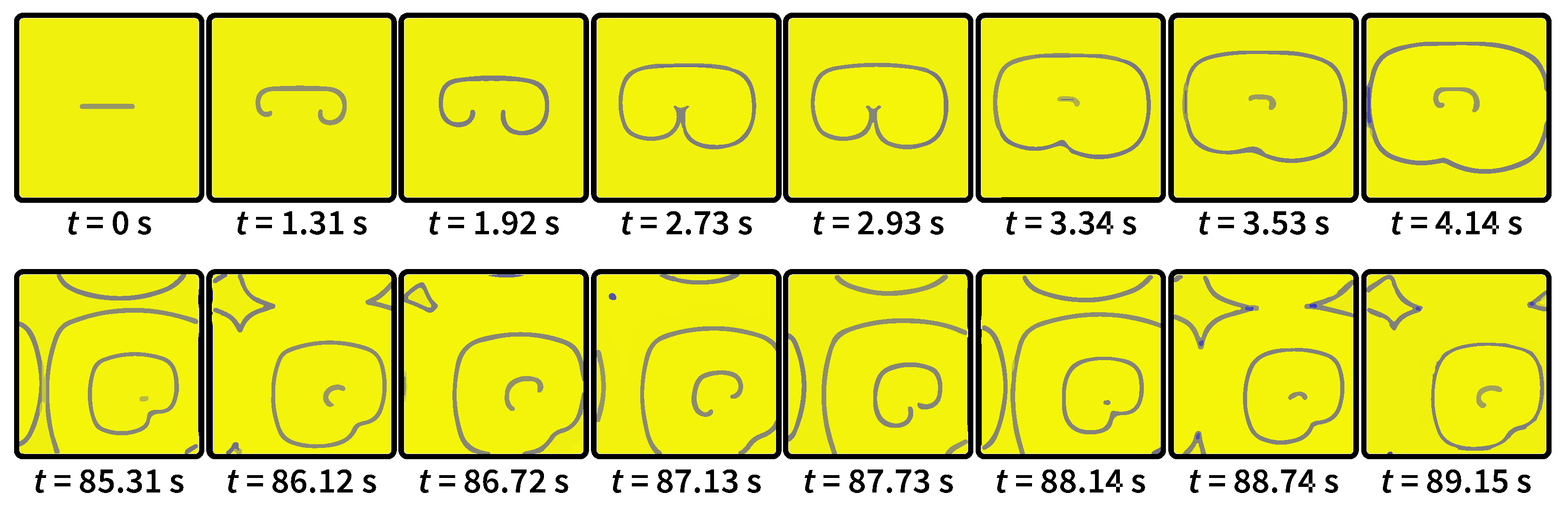
3.1.1. 1-D Reaction-Diffusion Medium with Memristors

Initially, the behavior of a memristor-based Oregonator model shown in Figure 4a is presented. The following equations summarize the dynamics of the presented model:
d u i d t = g u w i l u i 1 u i + g u w i r u i + 1 u i Δ x 2 + f u ( · ) d v i d t = f v ( · )
where g u ( · ) is the monotonically increasing function of (3) that corresponds to the conductance of the memristor device.
g u w i l , r = g m i n + g m a x g m i n · 1 1 + e β w i l , r
where β is the gain, g m i n and g m a x are the minimum and maximum coupling strengths, respectively, and w i l , r are the variables for determining the coupling strength of the ith Oregonator (l: left, r: right). Finally, the following equation is describing the variation of the coupling strength through the derivative of w i l , r as shown in (4):
τ d w i l , r d t = g u w i l , r · η 1 · u i 1 , i + 1 u i
where the right-hand side of (4) represents the current of the memristors and η 1 correspond to the polarity coefficient ( η 1 = +1: w i l , η 1 = −1: w i r ).
A periodic pulse sequence was applied to stimulate one side of the boundary, with the conductance of the memristor being measured. The memristor’s initial conductance was set to zero and the simulated results are shown in Figure 4c. During the activation of the input pulse, the conductance was significantly increased, resulting in a slight rise in conductance. The difference in conductance ( Δ g ) per one pulse can be estimated to be 0.17 mS/pulse. Figure 4b depicts the simulation setup where the polarity of the memristor is inverted and consequently, the input pulses should cause the conductance to drop. The initial conductance was set so that stimulations to u 0 might generate chain excitation on u 1 through the memristor. The temporal responses of u 1 are shown in Figure 4d. As it can be observed the stimulus was initially applied to u 1 , but its oscillation was terminated because of the decrease in the conductance. It is noteworthy that the Neumann boundary condition is used in both of Figure 4a,b models.
The simulation results of a 1-D medium with 100 Oregonator elements without evoking a change in the conductance of the memristors are shown in Figure 5a. Both Oregonator circuit elements placed at the boundaries of the medium were stimulated at the same time, with the propagating waves colliding in the middle while neglecting each other. When memristive effects were applied, the findings were different from those illustrated in Figure 5a because the coupling strength g u ( w i l , r ) is affected by the direction of wave traversal. The results of simulating a 1-D architecture containing 100 Oregonator elements where the resistance of the memristor is changing based on the propagating waves are shown in Figure 5b. Because of the polarity of memristors, excitable waves going rightward raised w i l , r of the memristors to constitute the wave, whereas waves traveling leftward decreased w i l , r memristors. Consequently, the velocity of each excitable wave varied based on the direction of wave propagation, resulting in wave collision at a location other than the middle of the substrate, as it can be observed at t = 124 s of Figure 5b.
On the 1-D memristive media, a significant nonlinear feature, i.e., the formation of stationary spiral patterns has been observed. A total of 100 Oregonator elements were linked by memristors with a cyclic boundary condition in the simulations. The polarity of all the memristors was the same. An excitable wave propagated across the medium in a cyclic-looping way after stimulating one node (the 58th node as depicted in the simulation results shown in Figure 6). Wave propagation was adjusted to be unidirectional during the initial stimulation by setting proper refractory states of the Oregonator elements. The memristors’ initial conductance was set at g m i n . The time evolution of the conductance of each node ( u i ) is shown in Figure 6, with the magnitudes indicated by yellow-blue scale tones. Over time, spatial (nonuniform) patterns emerged. The produced patterns were periodic, similar to Turing patterns, and achieved equilibrium in roughly 2 × 10 4 s.

3.1.2. 2-D Reaction-Diffusion Medium with Memristors

In this section, the dynamic behavior of a 2-D memristive medium has been investigated. A grid of 100 × 100 Oregonator elements was simulated with a cyclic boundary condition. Additional memristive dynamics for w i u p , d for upward and downward connections are introduced for the 2-D RD medium, constituting a non Neumann neighborhood:
τ d w i u p , d d t = g u w i u p , d · η 2 · u i 1 , i + 1 u i
where w i u p , d denotes the variables for determining the coupling strength of the ith Oregonator element (up: upward, d: downward) and η 2 , the polarity coefficient ( η 2 = + 1 : w i u p , η 2 = 1 : w i d ). In the following simulations, one may assume both the polarity coefficients η 1 in Equation (5) and η 2 to be −1.
Initially all the Oregonator elements was set to inactive state. The excitable waves spread outwards when the node in the middle of the grid was stimulated, leading in the formation of patterns of ocean surface waves. The time evolution of each node ( u i , j ) ( u i , j = 0 : yellow, u i , j = 1 : blue) is depicted in Figure 7. The wave propagation velocity was delayed based on the wave propagation direction. According to the polarity of the memristors ( η 1 , η 2 = 1 ), the conductance of those on the right-hand side and below would rise, while those on the left-hand side and above would decrease. Consequently, the waves would collide on the left-hand side and upward. The conductance of all nodes is shown in Figure 8, with the conductance values indicated by yellow-blue color tones. Given that the conductance changes significantly as the wave propagates, these results were displayed while the conductance condition was stable. The change in conductance was still minimal after the waves propagated 10 times, but after the waves propagated 20 times at the location where the waves formed at the start and collided, the memristor conductance changed dramatically (Figure 8a). Figure 8b depicts the conductance of all nodes over a sufficient time period.
The initial stimulation was then adjusted by manipulating the states of the Oregonator elements, rather than using external stimuli. Inactive Oregonator elements were initially set in a refractory condition ( u i , j = 0 : yellow, u i , j = 1 : blue) as shown in Figure 9. The nearby Oregonator elements in the refractory condition suppressed the inactive Oregonator elements. Consequently, when the inactive Oregonator elements were in an active or inactive state, the wave rotated inwards, which resulted in the generation of clockwise and counterclockwise spiral patterns. Depending on the direction of wave propagation, the velocity of the rightward and downward waves was faster than that of the leftward and upward waves, given that η 1 in Equation (4) and η 2 = 1 in Equation (5) are both −1. Over time, the initial position of the generated waves, is moved to the lower right.

3.2. M-RLC Circuit Equivalent of a Chemical Medium

In this implementation [78], the R L C circuits are utilised as a transmission line equivalent to satisfy the essential conditions for the wave propagation application of a BZ membrane. The R L C units are designed in combination with the nonlinear dynamics of the memristors to expand the local non-linearity of BZ medium.
The utilized memristor model is a behavioral model of a voltage-controlled, threshold-type switching bipolar memristive device implemented in circuit-level [79]. The versatility of this generalized memristor model provides to circuit designers a powerful tool able to qualitatively reproduce the behavior of filamentary-based resistance switching, accurately fitting the response of the model to experimental data [80]. The following equations describe the aforementioned memristor’s dynamics:
r ˙ = a R s t · V M e m + V R s t c + | V M e m + V R s t | , V M e m < V R s t β · V M e m , V R s t V M e m V S e t a S e t · V M e m V S e t c + | V M e m V S e t | , V M e m > V S e t
x = x 0 · 1 m r
R ( x ) = 1 G ( x ) = f 0 · e 2 x x
Further details regarding the model and their parameter selection can be examined in [79].
For the proper wave propagation, each end of the M- R L C module (Figure 10) is connected to an adjacent one to form a 2-D transmission line. The wave propagation is occurring through a voltage stimuli, which is applied in an edge of the grid and is transmitted through the medium. To visualize this propagation, the voltage across each capacitor is displayed.

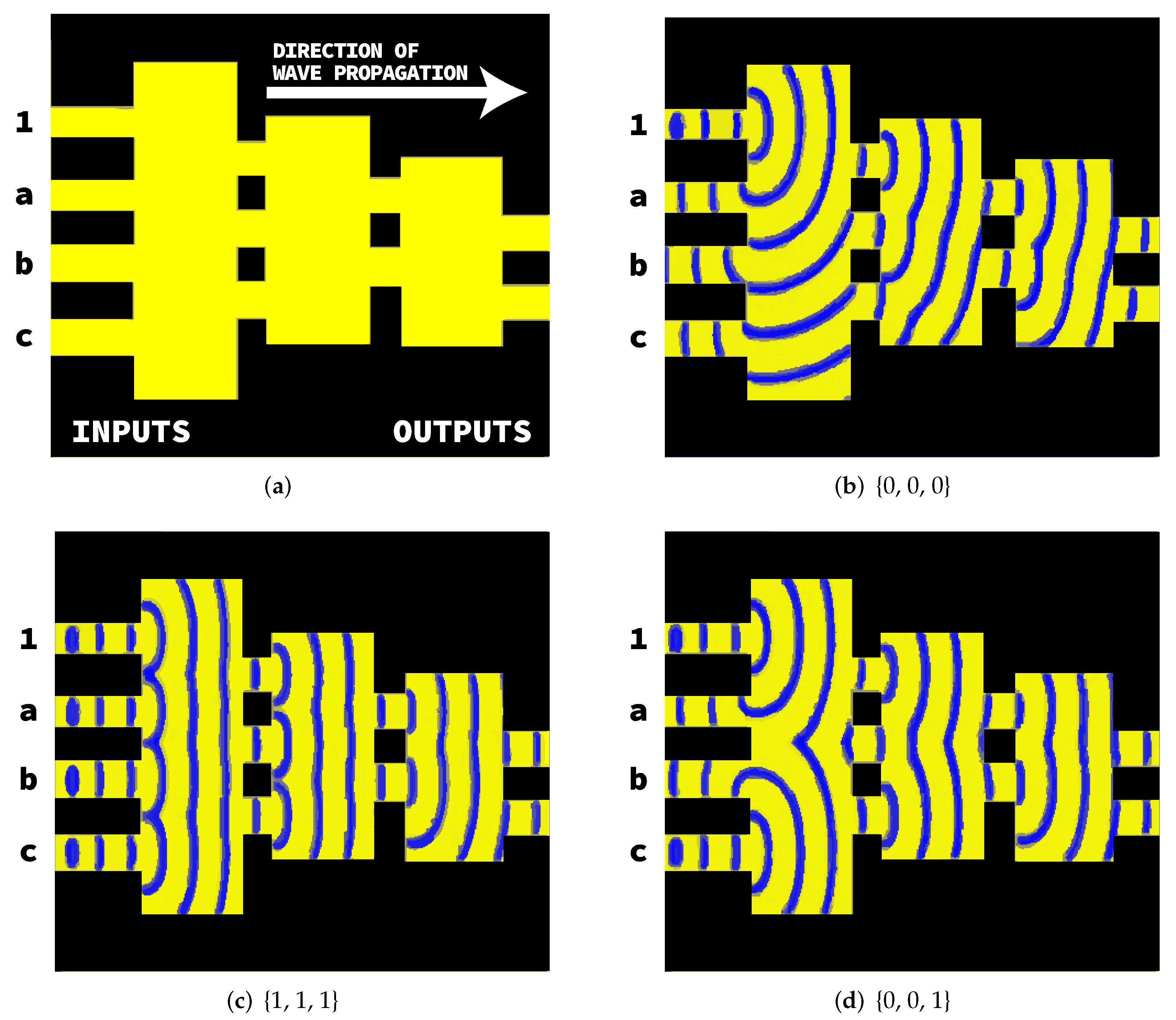
3.2.1. Wave Gates Implementation

The chemical-based 2-input NOR and XNOR logic gates [23] have been implemented to verify the operation of the suggested M- R L C circuit. The logical gates were designed on a 111 × 50 M- R L C grid with two output channels of 5 × 50 M- R L C units each, as it can be observed in Figure 11. The time difference between the incoming waves in the output channels is remaining constant and defines the logical output of the gate, in correspondence to the chemical gates’ output mechanism. The output is True or False depending on whether the propagating waves exit synchronously or asynchronously from the two output channels located on the right of the grid.
While the grid architecture of both gates remains unchanged, the positions of the input signals { x , y } are differentiated to implement each gate. In case of the NOR gate, the location of the two-input signals can be found on two neighboring M- R L C modules, and regarding the XNOR gate both input signals M- R L C modules are located in equal distance from signal ‘1’. In both cases, there is an always-triggered signal ‘1’ on the same distance from the output channels in case of both input signals absence to produce the required synchronized output. For all input combinations, the excitation of the M- R L C grid and the propagation time difference of the output channels, as well as the accurate location of the inputs, are illustrated in Figure 11.

3.2.2. An Alternative Approach

A different approach is proposed to overpass the complicated double channel output mechanism of the aforementioned examples, in which the logical result was determined by the timing difference of the two output waves. A new approach is therefore being presented to introduce wave-based logical gates on the same medium as previously with the ability their output to be defined as the existence (logical ‘1’) or lack (logical ‘0’) of a voltage amplitude at a certain time in the output’s side ( Z R , 1 : m ). An example of a 2-input NAND logic gate as an M- R L C implementation is provided requiring two steps to function, one for writing and one for reading, which take place in different areas of the grid. The write event includes the stimuli of the input signals { x , y } applied on the center of the M- R L C grid, while the read event includes the output read and grid reset procedures.
The input signals { x , y } are negative half-period sinusoidal and are applied in a limited area of V U and V D , respectively, to modify the memristance values of some M- R L C modules. When none or just one is applied, the propagating waves are not strong enough to alter the high memristance. On the other hand, when both input signals are applied simultaneously the two propagating waves collide and their cumulative amplitude succeed on switching the memristors to low memristance. At the same time, a full-period sinusoidal signal delayed by 180 degrees is applied on V L , 1 : m for the read event. This signal propagates across the medium and is low enough in amplitude in order to ensure that it will not arouse a change in the memristors’ resistance. If a part of the medium is in low memristance state due to the input signals, the first half of the read signal cannot reach the output loads (logical ‘0’). The second half of the read signal then propagates through the medium resets the grid to high memristance and prepares it for the next logic operation.
Figure 12 presents the function of the NAND gate when both inputs are applied ( { x , y } = ( 1 , 1 ) ). According to Figure 12a the input signals are applied (top) with the effect on memristors resistance (bottom), while a read/refresh signal is spread via the medium. Figure 12c shows the low amplitude negative read signal reaching the output, followed by the refresh signal that resets the memristors of the grid to high resistance state. All input combinations are illustrated in Figure 13 for the corresponding t 1 (top) and t 3 (bottom) frames proving that the negative half of the reading signal is reaching the output channel in all other cases except { x , y } = ( 1 , 1 ) , showcasing the correct operation of an NAND gate.

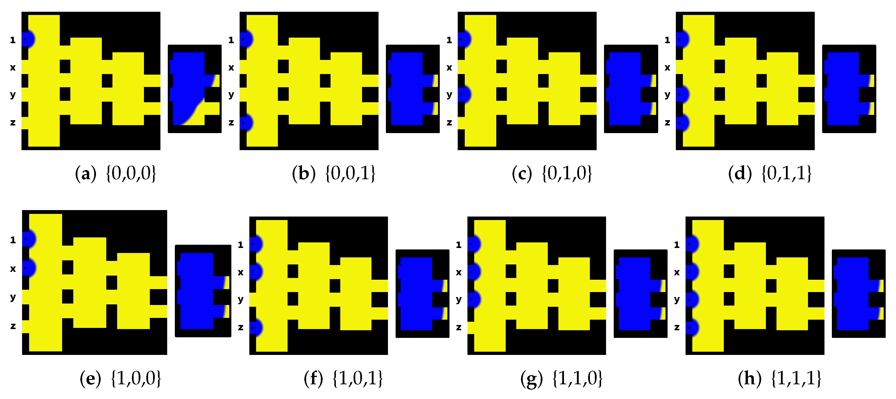
3.3. Memristive CA Cell for a Chemical Medium Representation

In order to address the shortest path problem, an electronic circuit based on memristors has been developed inspired by Physarum Polycephalum [81,82] simulating the spreading and shrinking of the latest during the vegetation phase while carrying out biochemical oscillations. Inspired by such a system, a memristive CA is proposed [83] to mimic the function of chemical logic gates while it manages to find the quickest propagation path to optimize gate’s area. The CA consists of a normal 2-D grid of N × M M e m C A modules interacting with the 8 nearest adjacent or diagonal neighbors (Figure 14) as specified by the well-known Moore neighborhood. More specifically, each M e m C A cell is described by a set of variables that constitute the CA cell state and is defined as follows:
C i , j t = { C e l l _ S t a t e , V O U T , F N , S t a t u s }
where the variable C e l l _ S t a t e defines if a cell is A c t i v e or I d l e , F N indicates the first neighbor that can provoke the activation of the current cell. The flag S t a t u s denotes the cells with specific role, like sources, and can be one of the following { N o r m a l , S o u r c e , D e s t i n a t i o n } , whilst V o u t is the output voltage of the cell’s M- R L C circuit. The combination of these variables governs the interaction of the current cell with its neighboring cells. Furthermore, the time evolution of the CA is discrete also in time and is described by a set of rules R.
In order to simulate the behavior of chemical logic gates, a M e m C A grid is used to map the topology of the respective gate. The inputs of the gate are designated as S o u r c e cells and the outputs as D e s t i n a t i o n cells, while the propagation medium as N o r m a l cells and the peripheral non-medium are constantly disabled cells. The S o u r c e cells are activated according to the required input during the spreading phase and the activation is spread until all output channels are active. The output of the gate is considered as ‘1’ or ‘0’ according to whether or not the excitation waves reach the two output channels synchronized or asynchronized. During the reduction phase of the proposed M e m C A , the activated area is being reduced in order to optimize the respective gate according to the shortest paths necessary that will remain.

3.3.1. MemCA Chemical Gates

Two M e m C A topologies have been designed for different chemical logic gates—a 2-input NOR, which is a functionally complete Boolean gate, and a 3-input OR—with their respective proof of concept. Figure 15 illustrates the suggested NOR gate design in a 100 × 50 M e m C A grid. Excitable M e m C A cells are colored as yellow defining the gate’s geometry, while the signal propagation is colored as blue and calculated by measuring the memristance of each cell. There are three input channels to the left of the gate including the two input signals { x , y } plus an always-triggered signal which is at an equal distance from both output channel to give the necessary synchronized output when both input signals be absent. The propagation evolution for each combination of the inputs is shown in Figure 15a–d, verifying the correct operation of the NOR gate by the synchronous output to be noticed only during the { 0 , 0 } inputs.
Regarding the more complex case of the 3-input OR gate, it is presented in a 100 × 100 M e m C A grid. On the left of the gate, four input channels can be observed, the first one is the always-triggered like an enable signal, while the rest are the input signals { x , y , z } . The propagation evolution for every input combination is presented in Figure 16, in which it is evident that only during { 0 , 0 , 0 } input, asynchronous output can be observed, matching the proper operation of a 3-input OR logic gate. The latest is more evident through the time difference of the propagating signal to reach the two output channels which can be examined in Figure 17.

3.3.2. Area Optimization

While the signal propagates from cell to cell at a constant pace as presented previously, the spread will reach the output channels initially through the shortest path. Therefore, without compromising the gate’s functionality, the area of the medium that does not fit the shortest way may be deleted. Because of the memristive circuit ability to calculate the shortest path, only cells that form the shortest routes from each input to each output can constitute the reduced area of the respective gate. To design such optimal gate, each input is initialized successively, and the shortest path is generated from the appropriate input to both output channels as seen in Figure 18a. Figure 18b was derived by overlaying the resulting paths for the respective input activations. Finally, the area of the optimized gate is conceived in Figure 18c with keeping only the region surrounding the overlaying shortest paths. Figure 19 illustrates the function of the improved OR logic gate in which its function has remained as intended despite the area reduction and the geometry change.

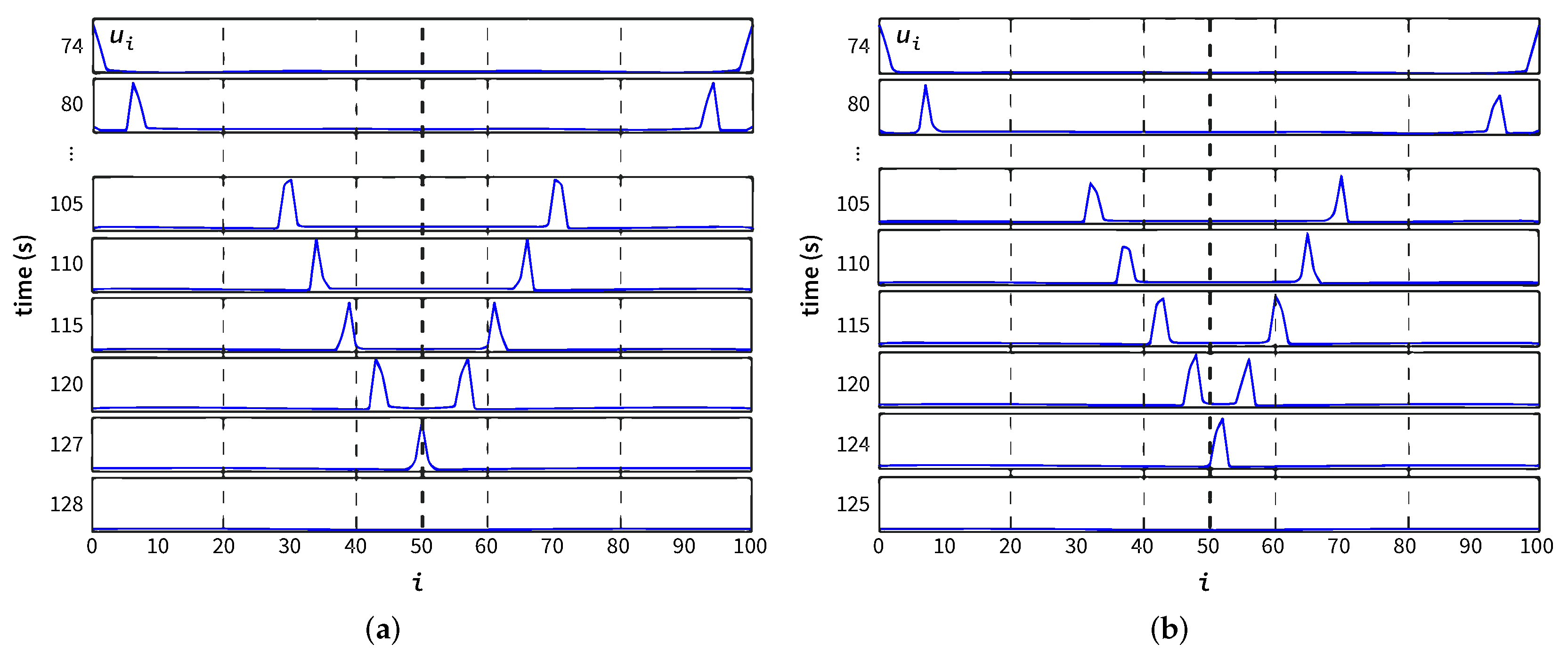
3.4. MemRC Oscillator for Chemical Wave Propagation Modeling

The oscillation of a memristor-resistor-capacitor ( M e m R C ) circuit under the constant power supply can be accomplished by combining the unipolar switching dynamics of the memristive device threshold switching regime with the charging-discharging behavior of a resistor-capacitor circuit module [84]. In order to integrate the threshold switching behavior of the fabricated CBRAM device of [85] in the circuit simulation, a modified version of the VTEAM model [86] has been implemented as described in [84].
Regarding the operation of the M e m R C oscillator under power supply, the memristor in the M e m R C oscillator forms the following voltage divider along with the resistor R O S C :
V E Q , h i g h = V P S C · M O F F ( R O S C + M O F F )
and capacitor voltage increases slowly from zero to V E Q , h i g h . However, having V O N < V E Q , h i g h , memristor’s SET process is triggered before the oscillator reaches the equilibrium and a new equilibrium point is defined as follows:
V E Q , l o w = V P S C · M O N ( R O S C + M O N )
resulting to capacitor voltage slowly decrease towards it. Afterwards, having V O F F > V E Q , l o w , memristor’s RESET process is triggered before capacitor voltage reaches V E Q , l o w and then oscillator’s equilibrium point becomes V E Q , h i g h . Thus, M e m R C is continuously oscillating between V O N and V O F F , as it is shown in the end of the plot of Figure 20b.
Beyond the oscillating part, the M e m R C features are extended by the power supply control circuitry. More specifically, the power supply control module consists of a set of parallel switches ( S i | i = [ 1 , N ] N N ) that allow the external activation of M e m R C power supply ( V H I G H ), along with a constantly connected branch ( V L O W R L O W ) that maintains oscillator voltage-level near the activation. The control of M e m R C activation is illustrated at the beginning of the plot of Figure 20b, where the signal V E X T activates M e m R C only in certain time.

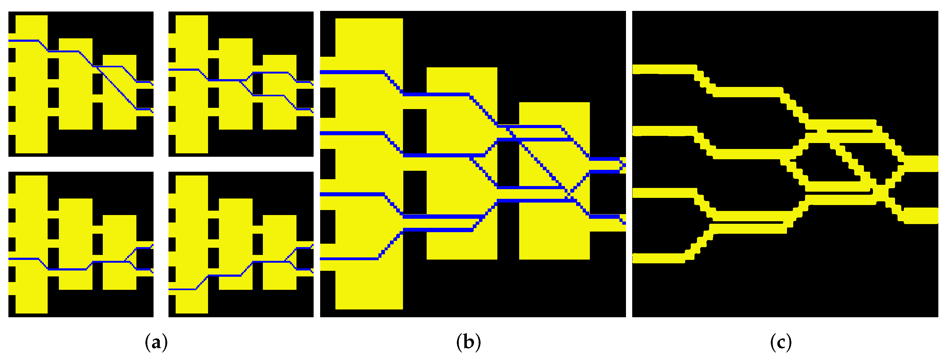
3.4.1. Topological Boolean Gates

Three possible logic gates topologies were created, namely OR, AND and NOT, using the M e m R C oscillator network inspired by the function of chemical logic gates. These gates comprise a universal set capable of replicating any Boolean operation. The output of the gate is interpreted as ‘1’ or ‘0’ if the oscillation spreading reaches the two output nodes at the same time or not following the respective chemical logic applications.
Figure 21 illustrates the suggested topology for the various gates in the M e m R C oscillator network. For OR and AND gates, which are 2-input gates, the input oscillators are noted with blue color and a respective variable. An a l w a y s 1 input oscillator noted in blue color can be spotted in Figure 21a–c, which is an always-activated input signal placed at a certain distance from either output node in order to provide the expected result in case of absence of both input signals. The computation results of ‘1’ or ‘0’ are determined by the synchronous or asynchronous propagation of the output node oscillation.
Each combination for the mentioned topologies inputs is shown in the Figure 21d–f. For OR gate, the asynchronized outputs can only be spotted during the { 0 , 0 } input combination, clearly matching the proper 2-input OR logic gate function. Synchronized outputs can be observed for AND gate only during { 1 , 1 } input combination. Lastly and for the case of NOT gate, only for { 0 } input synchronized outputs are noticed.

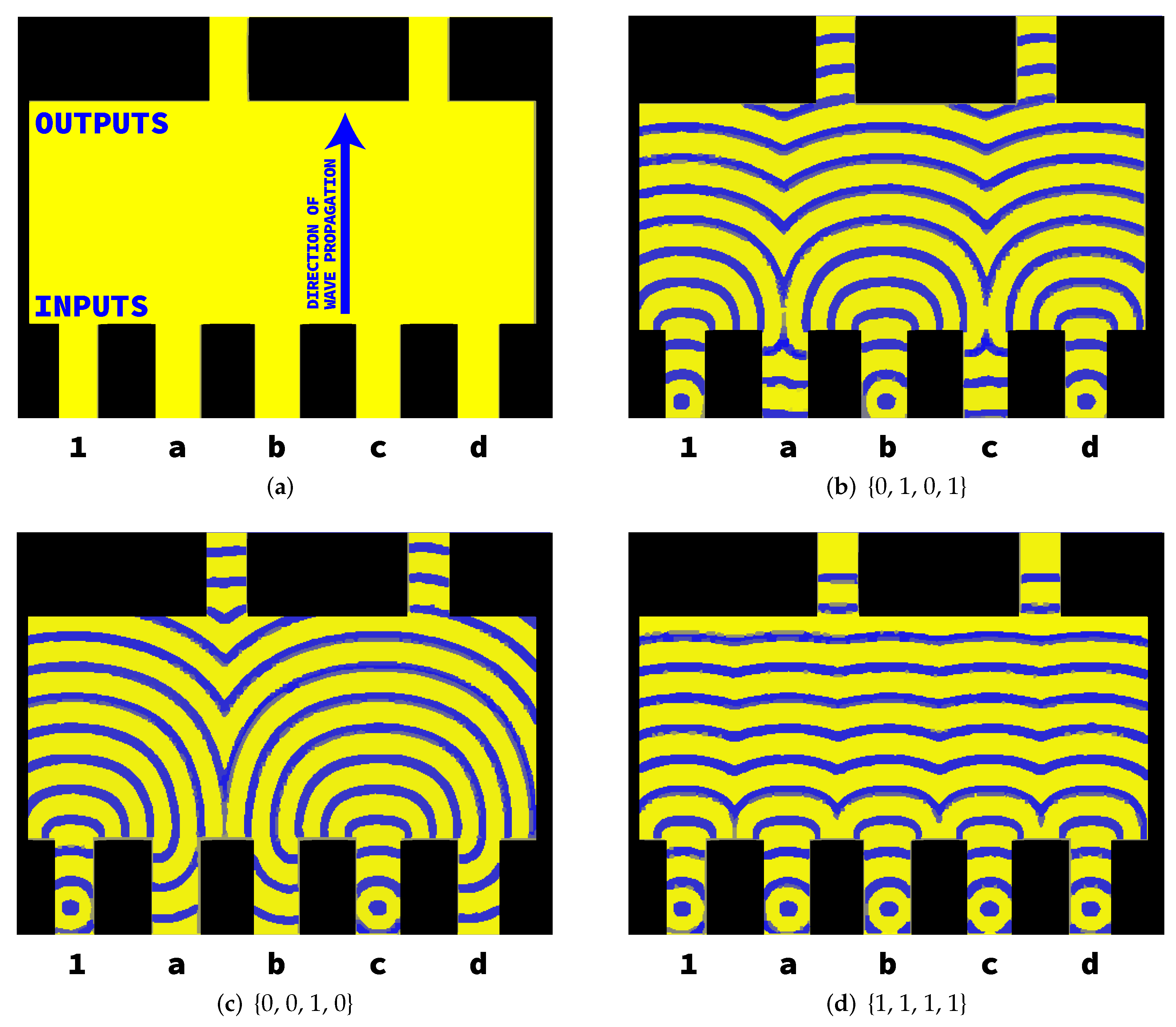
3.4.2. Multifunctional Gate

A multi-functional grid can be designed to concurrently implement a variety of logic gates using a series of properly connected M e m R C oscillators [87]. A multifunctional gate with 5 input oscillators (INPUT 1-5 ) and 2 output ones (OUTPUT 1-2) is presented in Figure 22a illustrating an appropriate spatial configuration inspired by chemical computing. For the proposed topology, each M e m R C oscillator is linked with the V o s c of its neighboring ones through the switches. Thus, if an oscillator is triggered and an oscillation is activated, it propagates to its adjacent and a wave front is spatially transmitted through the stimulating oscillations. To interpret the logic gate output, it is essential to monitor the signals in the two output nodes. In case of synchronization, it is a logical ‘1’, and in case of non-synchronization, it is a logical ‘0’.
The multifunctional M e m R C gate can be configured as one of the logic gates in Table 1 by selecting the proper input combination. Either one or two logic inputs, according to the needed inputs of each logic gate, are utilized as input signals, while a third is considered as a logical ‘1’ selector for the respective chemical gate, and the rest are considered as a logical ‘0’. Regarding the inputs, logical ‘0’ is equivalent to lack of signal, whereas ‘1’ is an excitation voltage pulse.
Figure 22b illustrates the activation time of the output nodes for the available gates of Table 1, which conform to the time when the oscillation reaches the highest voltage. Regarding the AND case, only for { 1 , 1 } input, outputs activation is simultaneous. Regarding the OR gate, every combination but { 0 , 0 } leads to the synchronous activation of the output nodes, exactly opposite of the NOR gate. For the XNOR gate, in case of { 0 , 0 } and { 1 , 1 } the outputs are synchronized. Based on the respective truth tables of each gate, the synchronization of the output nodes is the predicted one, thus the successful propagation of oscillations is verified, along with the proper operation of the multifunctional M e m R C gate.

4. Discussion & Conclusions

This review paper sums-up the research efforts for the design and simulation of wave propagating computing circuits that are based on the chemical equivalents, which can perform various computations exploiting the BZ reaction. The key component of these circuits is the integration of the memristor which enables the oscillatory behavior of the cell and consequently the wave propagation in a cell grid. By utilizing the memristor in the circuit, it was demonstrated that storing data as well as processing them can be combined in the same unit, while the circuit is properly mimicking the behavior of the chemical medium.
More specifically, the mathematical simulation of the reaction-diffusion rules that govern the chemical computers has been presented, utilizing the Oregonator model and Cellular Automata Oregonator model. Based on these simulations, which enabled a simpler and faster investigation into possible logic architectures, memristor-based wave propagating circuits have been designed that mimic the dynamics of the chemical computers. Memristive Oregonator elements as well as M e m R C oscillators have been developed and their suitability to perform Boolean computations was validated.
A valuable utilization of the examined circuits, following the implementation of Boolean logic, is to perform neuromorphic computations. By combining the signal propagation through wave-fronts with the memory capabilities of memristors it will be possible to develop a neuromorphic circuit capable of being trained and performing complex computations. The potential of chemical systems to perform computations was observed in nature a priori. Even human brains communicate through the diffusion of mediators and neuromodulators. Since the brain’s computing capability is exerted by chemical agents, it can be considered as an electrochemical computing system rather than an electrical one. Combining the high speed of electronic chips with the inherent processing power of chemical computing can result in a novel approach to artificial intelligence. Consequently, future research of the wave propagating and oscillating circuits revolves around performing neuromorphic calculations, in order to take advantage of the principles of distributed, parallel, and event-driven operations found in such computational systems. Through the wave propagating behavior of memristive oscillators, the design of a hardware equivalent to biological nervous system will be thoroughly investigated.
Following the present research results, the fabrication of the suggested M- R L C and M e m R C systems is seen as critical for the next step in electronic-based chemical computing circuits. The challenges foreseen towards this path include the effect of memristors’ variability to the system’s performance and functionality along with the sizes of the capacitors and inductors, which need further optimizations in order for the proposed systems to be able to compete in terms of speed with current state of the art classical computing systems. Nevertheless these drawbacks are offsetted by the distributed and simultaneous operations of these systems which provide fault tolerance and speedup through parallel processing of information. Further modifications to the proposed systems may be needed in order to deal with and overcome the mentioned demands.

Author Contributions

Conceptualization, T.P.C., I.-A.F., V.N., S.K., M.-A.T., P.B., D.T., A.A. and G.C.S.; methodology, T.P.C., I.-A.F., V.N., S.K., M.-A.T., P.B., D.T., A.A. and G.C.S.; software, T.P.C., I.-A.F., V.N., S.K., M.-A.T., P.B., D.T., A.A. and G.C.S.; validation, T.P.C., I.-A.F., V.N., S.K., M.-A.T., P.B., D.T., A.A. and G.C.S.; formal analysis, T.P.C., I.-A.F., V.N., S.K., M.-A.T., P.B., D.T., A.A. and G.C.S.; investigation, T.P.C., I.-A.F., V.N., S.K., M.-A.T., P.B., D.T., A.A. and G.C.S.; resources, T.P.C., I.-A.F., V.N., S.K., M.-A.T., P.B., D.T., A.A. and G.C.S.; data curation, T.P.C., I.-A.F., V.N., S.K., M.-A.T., P.B., D.T., A.A. and G.C.S.; writing—original draft preparation, T.P.C., I.-A.F., V.N., S.K., M.-A.T., P.B., D.T., A.A. and G.C.S.; writing—review and editing, T.P.C., I.-A.F., V.N., S.K., M.-A.T., P.B., D.T., A.A. and G.C.S.; visualization, T.P.C., I.-A.F., V.N., S.K., M.-A.T., P.B., D.T., A.A. and G.C.S.; supervision, T.P.C., I.-A.F., V.N., S.K., M.-A.T., P.B., D.T., A.A. and G.C.S.; project administration, T.P.C., I.-A.F., V.N., S.K., M.-A.T., P.B., D.T., A.A. and G.C.S.; funding acquisition, T.P.C., I.-A.F., V.N., S.K., M.-A.T., P.B., D.T., A.A. and G.C.S. All authors have read and agreed to the published version of the manuscript.

Funding

This work has been supported by the Hellenic Foundation for Research and Innovation (H.F.R.I.) under the “First Call for H.F.R.I. Research Projects to support Faculty members and Researchers and the procurement of high-cost research equipment grant” (Project Number: 3830).

Conflicts of Interest

The authors declare no conflict of interest.

References

  1. Banzhaf, W.; Dittrich, P.; Rauhe, H. Emergent computation by catalytic reactions. Nanotechnology 1996, 7, 307–314. [Google Scholar] [CrossRef] [Green Version]
  2. Adamatzky, A.; Costello, B.D.L.; Asai, T. Reaction-Diffusion Computers; Elsevier: Amsterdam, The Netherlands, 2005. [Google Scholar]
  3. Mikhailov, A.S.; Showalter, K. Control of waves, patterns and turbulence in chemical systems. Phys. Rep. 2006, 425, 79–194. [Google Scholar] [CrossRef]
  4. Gorecki, J.; Gizynski, K.; Guzowski, J.; Gorecka, J.N.; Garstecki, P.; Gruenert, G.; Dittrich, P. Chemical computing with reaction—Diffusion processes. Philos. Trans. R. Soc. A Math. Phys. Eng. Sci. 2015, 373, 20140219. [Google Scholar] [CrossRef] [PubMed] [Green Version]
  5. Gentili, P.L.; Giubila, M.S.; Germani, R.; Heron, B.M. Photochromic and luminescent compounds as artificial neuron models. Dyes Pigment. 2018, 156, 149–159. [Google Scholar] [CrossRef] [Green Version]
  6. Dueñas-Díez, M.; Pérez-Mercader, J. How chemistry computes: Language recognition by non-biochemical chemical automata. From finite automata to turing machines. Iscience 2019, 19, 514–526. [Google Scholar] [CrossRef] [Green Version]
  7. Foulon, B.L.; Liu, Y.; Rosenstein, J.K.; Rubenstein, B.M. A Language for Molecular Computation. Chem 2019, 5, 3017–3019. [Google Scholar] [CrossRef]
  8. Dueñas-Díez, M.; Pérez-Mercader, J. In-vitro reconfigurability of native chemical automata, the inclusiveness of their hierarchy and their thermodynamics. Sci. Rep. 2020, 10, 6814. [Google Scholar] [CrossRef] [Green Version]
  9. Bose, A.; Gorecki, J. Computing With Networks of Chemical Oscillators and its Application for Schizophrenia Diagnosis. Front. Chem. 2022, 10, 848685. [Google Scholar] [CrossRef]
  10. Egbert, M.D.; Gruenert, G.; Ibrahim, B.; Dittrich, P. Combining evolution and self-organization to find natural Boolean representations in unconventional computational media. Biosystems 2019, 184, 104011. [Google Scholar] [CrossRef]
  11. Dueñas-Díez, M.; Pérez-Mercader, J. Native Chemical Computation. A Generic Application of Oscillating Chemistry Illustrated With the Belousov-Zhabotinsky Reaction. A Review. Front. Chem. 2021, 9, 611120. [Google Scholar] [CrossRef]
  12. Parrilla-Gutierrez, J.M.; Sharma, A.; Tsuda, S.; Cooper, G.J.; Aragon-Camarasa, G.; Donkers, K.; Cronin, L. A programmable chemical computer with memory and pattern recognition. Nat. Commun. 2020, 11, 1442. [Google Scholar] [CrossRef] [PubMed]
  13. Przyczyna, D.; Zawal, P.; Mazur, T.; Strzelecki, M.; Gentili, P.L.; Szaciłowski, K. In-materio neuromimetic devices: Dynamics, information processing and pattern recognition. Jpn. J. Appl. Phys. 2020, 59, 050504. [Google Scholar] [CrossRef] [Green Version]
  14. Zaikin, A.; Zhabotinsky, A. Concentration wave propagation in two-dimensional liquid-phase self-oscillating system. Nature 1970, 225, 535–537. [Google Scholar] [CrossRef] [PubMed]
  15. Zhabotinsky, A.; Zaikin, A. Autowave processes in a distributed chemical system. J. Theor. Biol. 1973, 40, 45–61. [Google Scholar] [CrossRef]
  16. Winfree, A.T. The prehistory of the Belousov-Zhabotinsky oscillator. J. Chem. Educ. 1984, 61, 661–663. [Google Scholar] [CrossRef]
  17. Pechenkin, A. On the Origin of the Belousov-Zhabotinsky Reaction. Biol. Theory 2006, 4, 196–206. [Google Scholar] [CrossRef]
  18. Kiprijanov, K.S. Chaos and beauty in a beaker: The early history of the Belousov-Zhabotinsky reaction. Ann. Der Phys. 2016, 528, 233–237. [Google Scholar] [CrossRef] [Green Version]
  19. Mikhailov, A.S.; Ertl, G. The Belousov–Zhabotinsky Reaction. In Chemical Complexity: Self-Organization Processes in Molecular Systems; Springer International Publishing: Cham, Switzerland, 2017; pp. 89–103. [Google Scholar]
  20. Bartolomei, B.; Heron, B.M.; Gentili, P.L. A contribution to neuromorphic engineering: Neuromodulation implemented through photochromic compounds maintained out of equilibrium by UV–visible radiation. Rend. Lincei Sci. Fis. Nat. 2020, 31, 39–52. [Google Scholar] [CrossRef] [Green Version]
  21. Adamatzky, A. Collision-based computing in Belousov–Zhabotinsky medium. Chaos Solitons Fractals 2004, 21, 1259–1264. [Google Scholar] [CrossRef]
  22. Igarashi, Y.; Gorecki, J. Chemical Diodes Built with Controlled Excitable Media. Int. J. Unconv. Comput. 2011, 7, 141–158. [Google Scholar]
  23. Steinbock, O.; Kettunen, P.; Showalter, K. Chemical wave logic gates. J. Phys. Chem. 1996, 100, 18970–18975. [Google Scholar] [CrossRef]
  24. Sielewiesiuk, J.; Górecki, J. Logical functions of a cross junction of excitable chemical media. J. Phys. Chem. A 2001, 105, 8189–8195. [Google Scholar] [CrossRef]
  25. Egbert, M.; Gagnon, J.S.; Pérez-Mercader, J. From chemical soup to computing circuit: Transforming a contiguous chemical medium into a logic gate network by modulating its external conditions. J. R. Soc. Interface 2019, 16, 20190190. [Google Scholar] [CrossRef] [Green Version]
  26. Gorecki, J.; Yoshikawa, K.; Igarashi, Y. On chemical reactors that can count. J. Phys. Chem. A 2003, 107, 1664–1669. [Google Scholar] [CrossRef]
  27. Sun, M.Z.; Zhao, X. Multi-bit binary decoder based on Belousov-Zhabotinsky reaction. J. Chem. Phys. 2013, 138, 114106. [Google Scholar] [CrossRef]
  28. Zhang, G.M.; Wong, I.; Chou, M.T.; Zhao, X. Towards constructing multi-bit binary adder based on Belousov-Zhabotinsky reaction. J. Chem. Phys. 2012, 136, 164108. [Google Scholar] [CrossRef]
  29. Sun, M.Z.; Zhao, X. Crossover Structures for Logical Computations in Excitable Chemical Medium. Int. J. Unconv. Comput. 2015, 11, 165–184. [Google Scholar]
  30. Guo, S.; Sun, M.Z.; Han, J.D.; Zhao, X. Digital Comparator in Excitable Chemical Media. Int. J. Unconv. Comput. 2015, 11, 131–145. [Google Scholar]
  31. Stovold, J.; O’Keefe, S. Reaction–diffusion chemistry implementation of associative memory neural network. Int. J. Parallel Emergent Distrib. Syst. 2017, 32, 74–94. [Google Scholar] [CrossRef]
  32. Stovold, J.; O’Keefe, S. Associative Memory in Reaction-Diffusion Chemistry. In Advances in Unconventional Computing; Springer: Berlin/Heidelberg, Germany, 2017; pp. 141–166. [Google Scholar]
  33. Gorecki, J.; Gorecka, J.N. Information Processing with Chemical Excitations–from Instant Machines to an Artificial Chemical Brain. Int. J. Unconv. Comput. 2006, 2, 321–336. [Google Scholar]
  34. Gentili, P.L.; Horvath, V.; Vanag, V.K.; Epstein, I.R. Belousov-Zhabotinsky “Chemical Neuron” as a Binary and Fuzzy Logic Processor. Int. J. Unconv. Comput. 2012, 8, 177–192. [Google Scholar]
  35. Takigawa-Imamura, H.; Motoike, I.N. Dendritic gates for signal integration with excitability-dependent responsiveness. Neural Netw. 2011, 24, 1143–1152. [Google Scholar] [CrossRef] [PubMed] [Green Version]
  36. Stovold, J.; O’Keefe, S. Simulating neurons in reaction-diffusion chemistry. In International Conference on Information Processing in Cells and Tissues; Springer: Berlin/Heidelberg, Germany, 2012; pp. 143–149. [Google Scholar]
  37. Gruenert, G.; Gizynski, K.; Escuela, G.; Ibrahim, B.; Gorecki, J.; Dittrich, P. Understanding networks of computing chemical droplet neurons based on information flow. Int. J. Neural Syst. 2015, 25, 1450032. [Google Scholar] [CrossRef] [PubMed] [Green Version]
  38. Mallphanov, I.L.; Vanag, V.K. Chemical micro-oscillators based on the Belousov–Zhabotinsky reaction. Russ. Chem. Rev. 2021, 90, 1263. [Google Scholar] [CrossRef]
  39. Kuhnert, L.; Agladze, K.; Krinsky, V. Image processing using light-sensitive chemical waves. Nature 1989, 337, 244. [Google Scholar] [CrossRef]
  40. Rambidi, N.; Kuular, T.O.; Makhaeva, E. Information-processing capabilities of chemical reaction–diffusion systems. 1. Belousov–Zhabotinsky media in hydrogel matrices and on solid supports. Adv. Mater. Opt. Electron. 1998, 8, 163–171. [Google Scholar] [CrossRef]
  41. Rambidi, N.; Shamayaev, K.; Peshkov, G.Y. Image processing using light-sensitive chemical waves. Phys. Lett. A 2002, 298, 375–382. [Google Scholar] [CrossRef]
  42. Wang, Y.; Xie, Y.; Yuan, C.; Wang, H.; Fu, D. Intelligent image sensor based on probing the evolution of redox potentials distributed in reaction–diffusion medium. Sens. Actuators B Chem. 2010, 145, 285–292. [Google Scholar] [CrossRef]
  43. Adamatzky, A. Computing in Nonlinear Media and Automata Collectives; CRC Press: Boca Raton, FL, USA, 2001. [Google Scholar]
  44. Kuhnert, L. A new optical photochemical memory device in a light-sensitive chemical active medium. Nature 1986, 319, 393. [Google Scholar] [CrossRef]
  45. Adamatzky, A.; Tsompanas, M.A.; Draper, T.C.; Fullarton, C.; Mayne, R. Liquid Marble Photosensor. ChemPhysChem 2020, 21, 90–98. [Google Scholar] [CrossRef]
  46. Tsompanas, M.A.; Fyrigos, I.A.; Ntinas, V.; Adamatzky, A.; Sirakoulis, G.C. Light sensitive Belousov-Zhabotinsky medium accommodates multiple logic gates. BioSystems 2021, 206, 104447. [Google Scholar] [CrossRef] [PubMed]
  47. Pullela, S.R.; Cristancho, D.; He, P.; Luo, D.; Hall, K.R.; Cheng, Z. Temperature dependence of the Oregonator model for the Belousov-Zhabotinsky reaction. Phys. Chem. Chem. Phys. 2009, 11, 4236–4243. [Google Scholar] [CrossRef] [PubMed]
  48. Adamatzky, A.; Fullarton, C.; Phillips, N.; De Lacy Costello, B.; Draper, T.C. Thermal switch of oscillation frequency in Belousov–Zhabotinsky liquid marbles. R. Soc. Open Sci. 2019, 6, 190078. [Google Scholar] [CrossRef] [PubMed] [Green Version]
  49. Yokoi, H.; Adamatzky, A.; de Lacy Costello, B.; Melhuish, C. Excitable chemical medium controller for a robotic hand: Closed-loop experiments. Int. J. Bifurc. Chaos 2004, 14, 3347–3354. [Google Scholar] [CrossRef]
  50. Field, R.J.; Noyes, R.M. Oscillations in chemical systems. IV. Limit cycle behavior in a model of a real chemical reaction. J. Chem. Phys. 1974, 60, 1877–1884. [Google Scholar] [CrossRef] [Green Version]
  51. Beato, V.; Engel, H. Pulse propagation in a model for the photosensitive Belousov-Zhabotinsky reaction with external noise. In Proceedings of the SPIE’s First International Symposium on Fluctuations and Noise, Santa Fe, NM, USA, 1 June 2003; pp. 353–362. [Google Scholar]
  52. Gong, X.; Asai, T.; Motomura, M. Reaction-diffusion media with excitable oregonators coupled by memristors. In Proceedings of the 2012 13th International Workshop on Cellular Nanoscale Networks and Their Applications, Turin, Italy, 29–31 August 2012; pp. 1–6. [Google Scholar] [CrossRef]
  53. Berenstein, I.; Beta, C. Cross-diffusion in the two-variable Oregonator model. Chaos 2013, 23, 033119. [Google Scholar] [CrossRef]
  54. Pellitero, M.A.; Álvarez Lamsfus, C.; Borge, J. The Belousov–Zhabotinskii Reaction: Improving the Oregonator Model with the Arrhenius Equation. J. Chem. Educ. 2013, 90, 82–89. [Google Scholar] [CrossRef]
  55. Sherman, A.S.; Peskin, C.S. A Monte Carlo Method for Scalar Reaction Diffusion Equations. SIAM J. Sci. Stat. Comput. 1986, 7, 1360–1372. [Google Scholar] [CrossRef]
  56. Gerhardt, M.; Schuster, H.; Tyson, J.J. A Cellular Automaton Model of Excitable Media Including Curvature and Dispersion. Science 1990, 247, 1563–1566. [Google Scholar] [CrossRef]
  57. Weimar, J.R. Cellular automata for reaction-diffusion systems. Parallel Comput. 1997, 23, 1699–1715. [Google Scholar] [CrossRef]
  58. Masahiko, H.; Aoki, T.; Morimitsu, H.; Higuchi, T. Implementation of reaction-diffusion cellular automata. IEEE Trans. Circuits Syst. I Fundam. Theory Appl. 2002, 49, 10–16. [Google Scholar] [CrossRef]
  59. Ishimura, K.; Komuro, K.; Schmid, A.; Asai, T.; Motomura, M. FPGA implementation of hardware-oriented reaction-diffusion cellular automata models. Nonlinear Theory Its Appl. IEICE 2015, 6, 252–262. [Google Scholar] [CrossRef] [Green Version]
  60. Ushida, M.; Schmid, A.; Asai, T.; Ishimura, K.; Motomura, M. Motion Vector Estimation of Textureless Objects Exploiting Reaction-Diffusion Cellular Automata. Int. J. Unconv. Comput. 2016, 12, 169–187. [Google Scholar]
  61. Dourvas, N.I.; Sirakoulis, G.C.; Adamatzky, A. Cellular automaton Belousov–Zhabotinsky model for binary full adder. Int. J. Bifurc. Chaos 2017, 27, 1750089. [Google Scholar] [CrossRef] [Green Version]
  62. Tsompanas, M.A.; Fyrigos, I.A.; Ntinas, V.; Adamatzky, A.; Sirakoulis, G.C. Cellular automata implementation of Oregonator simulating light-sensitive Belousov–Zhabotinsky medium. Nonlinear Dyn. 2021, 104, 4103–4115. [Google Scholar] [CrossRef]
  63. Toth, R.; Stone, C.; de Lacy Costello, B.; Adamatzky, A.; Bull, L. Simple collision-based chemical logic gates with adaptive computing. Int. J. Nanotechnol. Mol. Comput. 2010, 1, 1–6. [Google Scholar] [CrossRef] [Green Version]
  64. Adamatzky, A.; De Lacy Costello, B.; Bull, L.; Holley, J. Towards Arithmetic Circuits in Sub-Excitable Chemical Media. Isr. J. Chem. 2011, 51, 56–66. [Google Scholar] [CrossRef]
  65. Field, R.J.; Winfree, A.T. Travelling Waves of Chemical Activity in the Zaikin-Zhabotinskii-Winfree Reagent. J. Chem. Educ. 1979, 56, 754. [Google Scholar] [CrossRef]
  66. Cassani, A.; Monteverde, A.; Piumetti, M. Belousov-Zhabotinsky type reactions: The non-linear behavior of chemical systems. J. Math. Chem. 2021, 59, 792–826. [Google Scholar] [CrossRef]
  67. Adamatzky, A. Fredkin and Toffoli gates implemented in Oregonator model of Belousov–Zhabotinsky medium. Int. J. Bifurc. Chaos 2017, 27, 1750041. [Google Scholar] [CrossRef] [Green Version]
  68. Asai, T.; Nishimiya, Y.; Amemiya, Y. A CMOS reaction-diffusion circuit based on cellular-automaton processing emulating the Belousov-Zhabotinsky reaction. IEICE Trans. Fundam. Electron. Commun. Comput. Sci. 2002, 85, 2093–2096. [Google Scholar]
  69. Matsubara, H.; Asai, T.; Hirose, T.; Amemiya, Y. Reaction-diffusion chip implementing excitable lattices with multiple-valued cellular automata. IEICE Electron. Express 2004, 1, 248–252. [Google Scholar] [CrossRef] [Green Version]
  70. Adamatzky, A.; Arena, P.; Basile, A.; Carmona-Galán, R.; Costello, B.D.L.; Fortuna, L.; Frasca, M.; Rodríguez-Vázquez, A. Reaction-diffusion navigation robot control: From chemical to VLSI analogic processors. IEEE Trans. Circuits Syst. I Regul. Pap. 2004, 51, 926–938. [Google Scholar] [CrossRef]
  71. Petrás, I.; Rekeczky, C.; Roska, T.; Carmona, R.; Jiménez-Garrido, F.; Rodríguez-Vázquez, A. Exploration of spatial-temporal dynamic phenomena in a 32 × 32-cell stored program two-layer CNN universal machine chip prototype. J. Circuits Syst. Comput. 2003, 12, 691–710. [Google Scholar] [CrossRef]
  72. Shi, B.E.; Luo, T. Spatial pattern formation via reaction-diffusion dynamics in 32/spl times/32/spl times/4 CNN chip. IEEE Trans. Circuits Syst. I Regul. Pap. 2004, 51, 939–947. [Google Scholar] [CrossRef]
  73. Asai, T.; Kanazawa, Y.; Hirose, T.; Amemiya, Y. Analog reaction-diffusion chip imitating Belousov-Zhabotinsky reaction with hardware oregonator model. Int. J. Unconv. Comput. 2005, 1, 123–147. [Google Scholar]
  74. Daikoku, T.; Asai, T.; Amemiya, Y. An analog CMOS circuit implementing Turing’s reaction-diffusion model. Signal 2002, 4, 14. [Google Scholar]
  75. Karahaliloglu, K.; Balkir, S. Bio-inspired compact cell circuit for reaction-diffusion systems. IEEE Trans. Circuits Syst. II Express Briefs 2005, 52, 558–562. [Google Scholar] [CrossRef]
  76. Serrano-Gotarredona, T.; Linares-Barranco, B. Log-domain implementation of complex dynamics reaction-diffusion neural networks. IEEE Trans. Neural Netw. 2003, 14, 1337–1355. [Google Scholar] [CrossRef]
  77. Asai, T. Reaction-Diffusion Media with Excitable Oregonators Coupled by Memristors. In Memristor Networks; Springer: Berlin/Heidelberg, Germany, 2014; pp. 625–635. [Google Scholar]
  78. Fyrigos, I.A.; Ntinas, V.; Sirakoulis, G.C.; Adamatzky, A.; Erokhin, V.; Rubio, A. Wave computing with passive memristive networks. In Proceedings of the 2019 IEEE International Symposium on Circuits and Systems (ISCAS), Sapporo, Japan, 26–29 May 2019; pp. 1–5. [Google Scholar]
  79. Vourkas, I.; Batsos, A.; Sirakoulis, G.C. SPICE modeling of nonlinear memristive behavior. Int. J. Circuit Theory Appl. 2015, 43, 553–565. [Google Scholar] [CrossRef]
  80. Sassine, G.; La Barbera, S.; Najjari, N.; Minvielle, M.; Dubourdieu, C.; Alibart, F. Interfacial versus filamentary resistive switching in TiO2 and HfO2 devices. J. Vac. Sci. Technol. B 2016, 34, 012202. [Google Scholar] [CrossRef]
  81. Ntinas, V.; Vourkas, I.; Sirakoulis, G.C.; Adamatzky, A. Modeling Physarum space exploration using memristors. J. Phys. D Appl. Phys. 2017, 50, 174004. [Google Scholar] [CrossRef]
  82. Ntinas, V.; Vourkas, I.; Sirakoulis, G.C.; Adamatzky, A.I. Oscillation-Based Slime Mould Electronic Circuit Model for Maze-Solving Computations. IEEE Trans. Circuits Syst. I Regul. Pap. 2017, 64, 1552–1563. [Google Scholar] [CrossRef]
  83. Fyrigos, I.A.; Ntinas, V.; Tsompanas, M.A.; Kitsios, S.; Sirakoulis, G.C.; Tsoukalas, D.; Adamatzky, A. Implementation and Optimization of Chemical Logic Gates Using Memristive Cellular Automata. In Proceedings of the 2020 European Conference on Circuit Theory and Design (ECCTD), Sofia, Bulgaria, 7–10 September 2020; pp. 1–6. [Google Scholar]
  84. Chatzinikolaou, T.P.; Fyrigos, I.A.; Ntinas, V.; Kitsios, S.; Bousoulas, P.; Tsompanas, M.A.; Tsoukalas, D.; Sirakoulis, G.C. Unconventional Logic on Memristor-Based Oscillatory Medium. In Proceedings of the 2021 10th International Conference on Modern Circuits and Systems Technologies (MOCAST), Thessaloniki, Greece, 5–7 July 2021; pp. 1–4. [Google Scholar]
  85. Bousoulas, P.; Sakellaropoulos, D.; Papakonstantinopoulos, C.; Kitsios, S.; Arvanitis, C.; Bagakis, E.; Tsoukalas, D. Investigating the origins of ultra-short relaxation times of silver filaments in forming-free SiO2-based conductive bridge memristors. Nanotechnology 2020, 31, 454002. [Google Scholar] [CrossRef] [PubMed]
  86. Kvatinsky, S.; Ramadan, M.; Friedman, E.G.; Kolodny, A. VTEAM: A general model for voltage-controlled memristors. IEEE Trans. Circuits Syst. II Express Briefs 2015, 62, 786–790. [Google Scholar] [CrossRef]
  87. Chatzinikolaou, T.P.; Fyrigos, I.A.; Ntinas, V.; Kitsios, S.; Bousoulas, P.; Tsompanas, M.A.; Tsoukalas, D.; Sirakoulis, G.C. Multifunctional Spatially-Expanded Logic Gate for Unconventional Computations with Memristor-Based Oscillators. In Proceedings of the 17th International Workshop on Cellular Nanoscale Networks and Their Applications, Catania, Italy, 29 September–1 October 2021; pp. 1–4. [Google Scholar]
Figure 1. (a) Petri dish with initial state of BZ. (b) First waves-fronts being formed. (c) Diffusion of waves throughout the Petri dish.
Electronics 11 01683 g001
Figure 2. (a) Chemical OR gate topology as proposed in [23]. (bd) Chemical waves propagation for different input combinations { a , b , c } .
Electronics 11 01683 g002
Figure 3. (a) Combinatorial logic gate [(a OR b) AND (c OR d)] topology as proposed in [23]. (bd) Chemical waves propagation for different input combinations { a , b , c , d } .
Electronics 11 01683 g003
Figure 4. (a,b) Two Oregonator elements connected via a memristor with different polarities. (c) The increase of the conductance with time for the circuit in (a). (d) Development of u 1 in (b), for u 1 originally activated by u 0 , and given that the conductance decreases with time, u 1 reaches the inactive state.
Electronics 11 01683 g004
Figure 5. Space and time evolution of the waves on the 1-d RD circuit comprised of 100 Oregonator elements and the connectivity achieved with (a) resistors or (b) memristors. (a) In the absence of the memristive characteristics of the circuit, the waves travel at the same speed and collide at the middle of the architecture. (b) Whereas, in the case of the memristive behavior being present the collision of the waves happens at the right side and close to the middle of the configuration.
Electronics 11 01683 g005
Figure 6. Space and time evolution of the conductance g of a 1-D excitable substrate with memristors, given a cyclic condition for the boundaries.
Electronics 11 01683 g006
Figure 7. Ocean-surface-wave patterns on 2-D media with memristors. Although the center was stimulated, wave propagated asymmetrically due to memristive effect with same polarity over the medium.
Electronics 11 01683 g007
Figure 8. Conductance map of memristors for 2-D media for ocean-surface-wave patterns; (a) early and (b) late maps.
Electronics 11 01683 g008
Figure 9. Clockwise and counterclockwise spiral patterns on 2-D media with memristors.
Electronics 11 01683 g009
Figure 10. (a) RLC circuit which corresponds to a transmission line and (b) the modified circuit including a memristor (R = 0.01 Ω , L = 1 mH, C = 10 μ F). (c) A 2D topology of the respective M- R L C circuits.
Electronics 11 01683 g010
Figure 11. Examples for NOR (ad) and XNOR (eh) gates geometries for the input (top) and result (bottom) frames of the wave propagation for each possible input { x , y } .
Electronics 11 01683 g011
Figure 12. Example of the NAND gate topology for { x , y } = {1,1}. Voltage (V) across capacitors C of each M- R L C circuit (top) and the respective memristances ( Ω ) (bottom) on 3 different time frames.
Electronics 11 01683 g012
Figure 13. Example of the NAND gate topology for each possible input { x , y } . Voltage (V) across capacitors C of each M- R L C circuit on the input ( t 1 ) frame (top) and the result ( t 3 ) frame (bottom).
Electronics 11 01683 g013
Figure 14. M e m C A cell circuit schematic.
Electronics 11 01683 g014
Figure 15. Example of a 2-input NOR gate chemical topology. Input (left) and result (right) time frames for each possible input { x , y } .
Electronics 11 01683 g015
Figure 16. Example of a 3-input OR gate chemical topology. Input (left) and result (right) time frames for each possible input { x , y , z } .
Electronics 11 01683 g016
Figure 17. Activation time of the output channels for the (a) 2-input NOR chemical logic gate and the (b) 3-input OR chemical logic gate examples.
Electronics 11 01683 g017
Figure 18. (a) Input to output shortest paths. (b) Compound of the resulted shortest paths. (c) Final proposed gate topology after the area optimization.
Electronics 11 01683 g018
Figure 19. Example of the 3-input OR gate optimized topology. Input (left) and result (right) time frames for each possible input { x , y , z } .
Electronics 11 01683 g019
Figure 20. (a) M e m R C cell circuit schematic composed of the power supply control (left) and the oscillator (right). (b) I-V characteristic of the memristor model. (c) M e m R C cell operation.
Electronics 11 01683 g020
Figure 21. Schematics for the examples of (a) OR, (b) AND and (c) NOT logic gates. Activation time of the output channels for the (d) OR, (e) AND and (f) NOT logic gates for each possible input.
Electronics 11 01683 g021
Figure 22. (a) Schematic of the multifunctional gate. (b) Activation time of the output channels for each possible logic operation and input combination.
Electronics 11 01683 g022
Table 1. Logic Gate Input Combinations for each Logic Operation.
LogicLogic Gate Inputs
OperationINPUT 1INPUT 2INPUT 3INPUT 4INPUT 5
NOTx‘1’‘0’‘0’‘0’
AND‘0’‘0’xy‘1’
ORx‘0’‘1’y‘0’
XNORx‘1’y‘0’‘0’
NOR‘0’‘1’‘0’xy
Publisher’s Note: MDPI stays neutral with regard to jurisdictional claims in published maps and institutional affiliations.

