Article

A Low-Power ADPLL with Calibration-Free RO-Based Injection-Locking TDC for BLE Applications

1
Research and Development Center of Healthcare Electronics, Institute of Microelectronics of Chinese Academy of Sciences, Beijing 100029, China
2
Beijing Key Laboratory of RFIC Technology for Next Generation Communications, Institute of Microelectronics of Chinese Academy of Sciences, Beijing 100029, China
3
University of Chinese Academy of Sciences, Beijing 100049, China
*
Authors to whom correspondence should be addressed.
Electronics 2022, 11(13), 1953; https://doi.org/10.3390/electronics11131953
Submission received: 9 June 2022 / Revised: 17 June 2022 / Accepted: 20 June 2022 / Published: 22 June 2022

Abstract

:
This paper proposes a low-power all-digital phase-locked loop (ADPLL) with calibration-free ring oscillator (RO)-based injection-locking time to digital converter (TDC) for BLE applications. The RO is reused as the delay cell of TDC, and the quantization step of TDC is always tracked with the RO period; hence no calibration is needed in this architecture. We adopt RO tuning to lower the injection-locking bandwidth so as to decrease the power consumption of the injection current. Moreover, the fractional part of phase error detection is turned down in the coarse tuning of ADPLL to save power. An LC-based digital-controlled oscillator (LCDCO) with a 6.4 nH inductor and a resistive bias is used to have a low power and better phase noise performance. The ADPLL is fabricated in 40 nm CMOS with a 1 V supply and consumes 1.4 mW when it is locked. The measured phase noise is −114 dBc/Hz at 1 MHz offset. The test results show significant power saving. Thus, it can be a promising candidate for BLE applications.

1. Introduction

With the increasing demand for the Internet-of-Things (IoT), Bluetooth Low-Energy (BLE) has become a popular solution for short-range communication of wireless applications, such as wearable devices, sensor monitoring platforms, and smart cities [1,2,3,4,5]. However, due to the limitations of application scenarios, BLE devices often have the characteristics of small volume and are easy to carry. Some even need to be implanted into the human body, which puts forward strict requirements for the battery life of these devices. The wireless communication module dominates the power consumption budget of the whole system [6]. Therefore, with a limited energy supply, the low-power wireless communication system design has become the most critical requirement of BLE devices. Thanks to the relatively simple FSK modulation, the architecture of the BLE transceiver is simplified. In a BLE transmitter, frequency modulation can be achieved by direct frequency synthesis through a phase-locked loop (PLL). Therefore, the frequency synthesizer and PA occupy most of the power consumption of the whole BLE transmitter. Among them, how to reduce the power consumption of the frequency synthesizer on the premise of meeting the requirements of phase noise has become the most challenging design.
An all-digital phase-locked loop (ADPLL) was used as a wireless communication module roughly a decade ago [7,8]. In recent years, the advantages of frequency synthesizers based on ADPLL have gradually emerged due to the development of CMOS technology, and it has become popular instead of the analog-based charge-pump phase-locked loop (CPPLL). Figure 1 shows four different architectures of ADPLL. The divider-based ADPLL [9,10,11] in Figure 1a will cause additional quantization noise due to the sigma-delta modulator (SDM) for fractional operation. Moreover, this structure also has the problem of noise up-conversion caused by the time to digital converter (TDC) and divider. The counter-based ADPLL [12,13,14,15,16] shown in Figure 1b uses TDC to generate the fractional phase error directly. Thus, the additional divider noise will be removed, and only reference noise will be up-converted by the frequency multiplication ratio N. However, in this structure, TDC consumes much more power because of the extra normalization circuit caused by PVT variations. Figure 1c shows the counter-based ADPLL with embedded TDC [17]. Using the polyphase output characteristics of the RO, RO is reused as the delay unit of TDC. In this way, the quantization step of TDC always follows the cycle of RO output. Therefore, no additional normalization operation is required, and the power consumption is reduced. Based on this architecture, an ultra-low-power BLE transmitter is designed in [15]. It uses an RO-based wide bandwidth ADPLL working at 600 MHz and multiplies the frequency to 2.4 G through the edge combiner (EC). However, the design has poor phase noise performance, which limits the application of this structure. Moreover, to shorten the detection range of high-speed TDC, some architectures adopt a DTC-assisted TDC structure [14], which successfully reduces the complexity of the TDC circuit and uses TDC snapshotting to reduce the sampling rate to the reference frequency. However, the mismatch and nonlinearity between DTC and TDC will introduce spurs. At the same time, both DTC and TDC need calibration, resulting in additional power consumption.
Based on the embedded TDC, this paper proposes a low-power ADPLL architecture, as shown in Figure 1d, which uses LC digital-controlled oscillators (LCDCO) to inject the RO, and RO acts as the delay unit of TDC for fractional error operation. At the same time, type-I ADPLL is used to reduce the power consumption in the locking process, and the fractional error detection is turned down in the coarse tune process of the system. We use frequency tuning of RO, which has a 10 MHz tuning step to reduce the power consumption of injection locking and hence the DNL of injection-locked TDC.
This paper is organized as follows: Section 2 gives the analysis of the injection-locked RO and the calibration-free TDC. Then the overall architecture and system-level design considerations of the proposed ADPLL are presented. Section 3 talks about the detailed circuit implementation of the key building blocks. Section 4 demonstrates the measurement results and the comparison to the state-of-the-art. Finally, Section 5 draws the conclusion of the entire work.

2. Analysis and Design

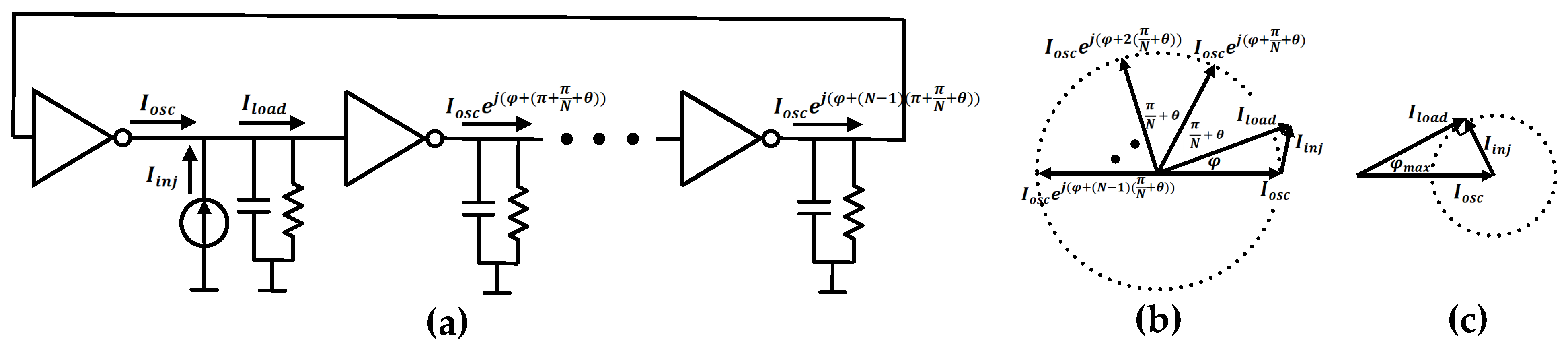
2.1. Analysis of Injection-Locked RO

The injection-locking technique is widely used in the design of frequency synthesizers, dividers, and voltage-controlled oscillators (VCO) [18,19,20,21]. Figure 2 shows a typical N-stage single-end RO and its current vector diagram; N must be an odd number to avoid circuit latch-up. I O S C is the RO current of each stage. To satisfy the Barkhausen criteria for oscillation, the overall phase shift of the oscillator loop must be an integer multiple of 2 π . Therefore, the RC-loading phase shift of each stage will be π / N . Its open-loop transfer function can be expressed as:
H ( j ω ) = A 0 N 1 + j ω R O ω B W N .
where A 0 is the low-frequency gain of each stage, ω R O is the free-running frequency of the RO, and ω B W is the 3-dB bandwidth of every signal stage. The relationship between oscillation frequency and the phase shift can be given by:
tan π N = ω R O ω B W .
As for the N-stage single-end RO under injection locking, the injection current I i n j is directly added to the first stage. The RO and its current vector diagram are shown in Figure 3. The phase condition of oscillation can be expressed as:
φ + N π N + θ + π = 2 k π .
where k = 1 , 2 , 3 , φ and θ are the additional phase shifts in the first stage and the remaining stages. After injection locking, the phase shift caused by RC-loading of every stage is ( π φ ) / N , so θ is equal to φ / N . With a constant strength of injection current I i n j , the maximum phase shift φ max will be satisfied when I i n j is orthogonal to the output current of the first stage ( I l o a d ). The current vector diagram is shown in Figure 3c.
We can infer from this diagram that:
I i n j sin φ max = I o s c sin ( π / 2 ) .
Similarly, combined with (2), the open-loop transfer function of RO under injection locking is given by:
H ( j ω ) = A 0 N 1 + j ω i n j ω B W N = A 0 N 1 + j ω i n j ω R O / tan π N N .
Therefore the phase shift caused by RC-loading of every stage can be expressed as:
tan 1 ω i n j ω R O / tan π N = π N + θ .
By applying Taylor’s formula, (6) can be approximated by:
θ Δ ω ω R O sin π N cos π N .
where Δ ω = ω i n j ω R O . Since | θ | is equal to | φ | / N , combining (7) and (4) we can infer that the injection locking bandwidth ω B W I L can be expressed as:
Δ ω ω R O 1 N 1 sin π N cos π N φ max = 1 N 1 sin π N cos π N sin 1 I i n j I o s c = ω B W I L ω R O .
From this expression, we can see that the injection locking bandwidth is related to the stages of RO and the injection current I i n j . Therefore, if a higher stage of RO is used, one can maintain the same ω B W by increasing I i n j .

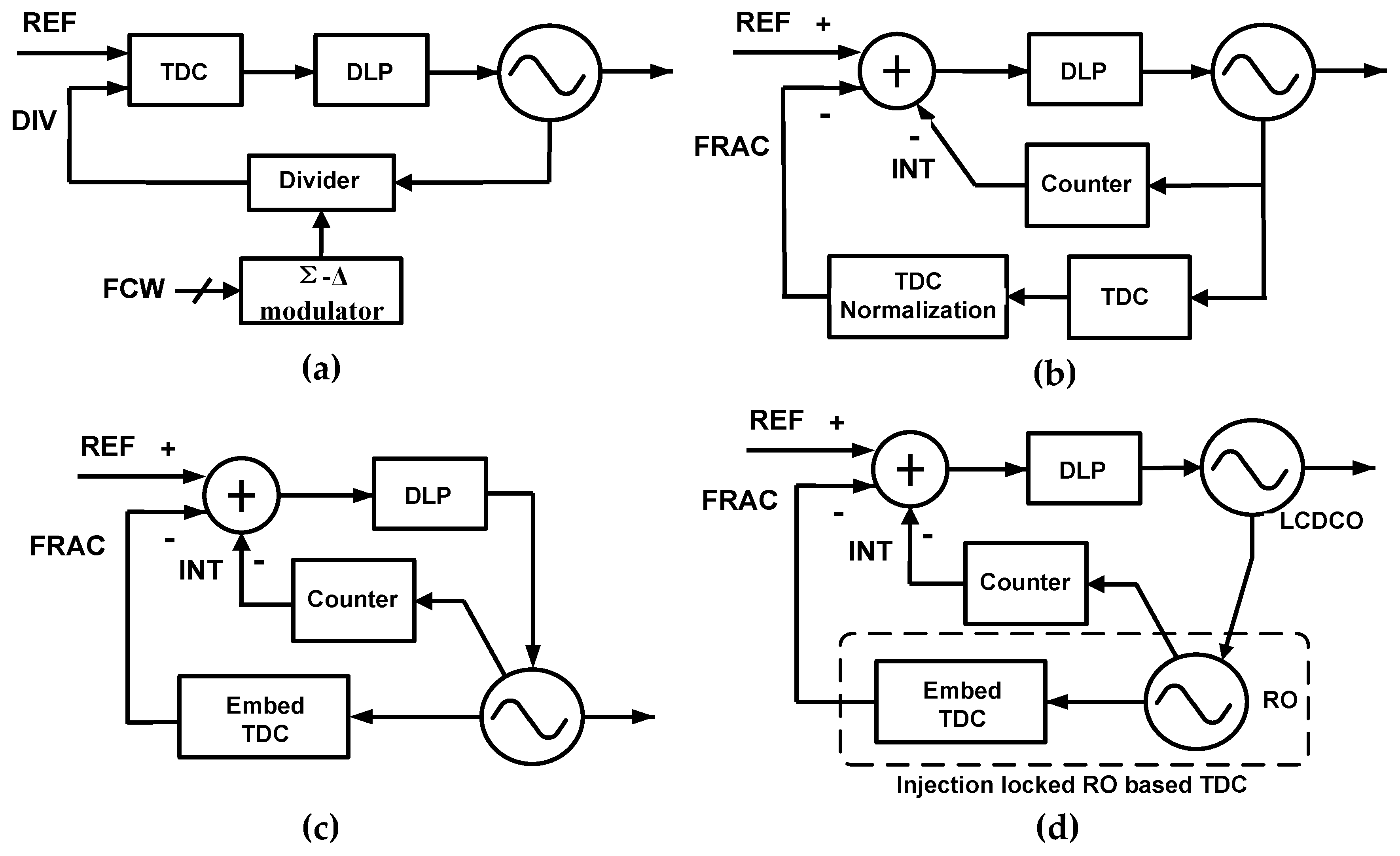
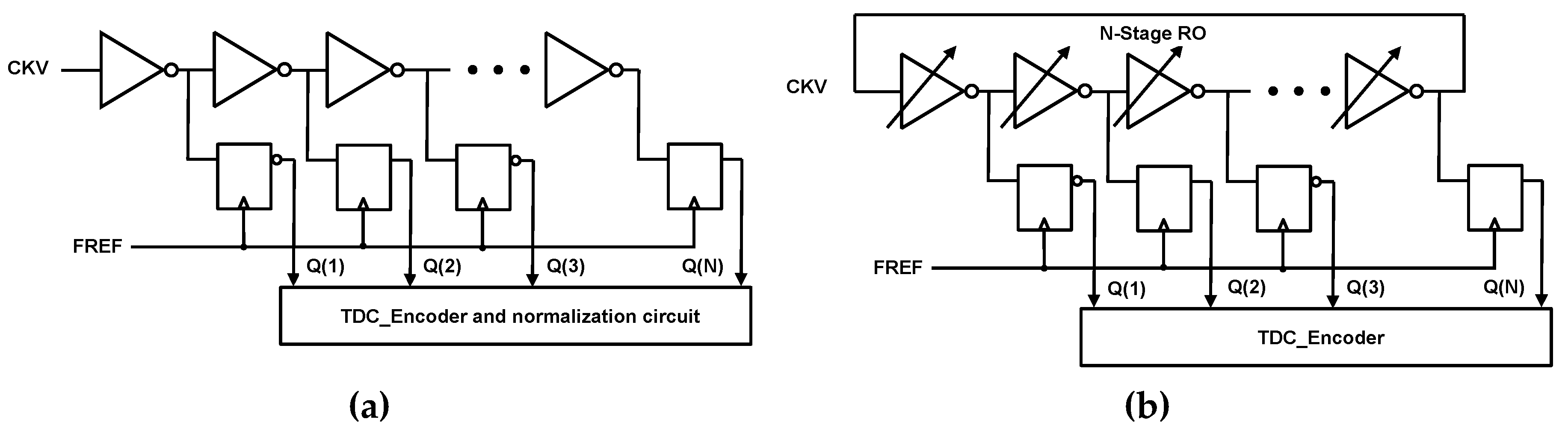
2.2. Calibration-Free RO-Based TDC

In counter-based ADPLL, TDC is used to quantize the time difference between the reference clock (FREF) and the DCO output clock (CKV). Figure 4a shows the structure of classical flash TDC. CKV passes through an inverter delay chain, and every output of the delay will be sampled by the same FREF. The output is then encoded and normalized to the range ( 1 , 1 ) since one cycle of CKV is normalized to 1. Nevertheless, because of the PVT variation, the TDC quantization step must be calibrated so as to catch the CKV period [8]. Thus, this is a relatively power-hungry choice. However, as shown in Figure 4b, if we reuse RO as the TDC’s delay chain, the flip flops directly sample every stage of the RO output. This structure is called embedded TDC [17]. In this situation, the TDC quantization step will always track with the CKV period, which means no calibration is needed, and the power consumption is saved.
As discussed in an earlier section, if RO is injection-locked, the phase shift among the stages of RO will be unequal, which will lead to differential nonlinearity (DNL) of the embedded TDC. The DNL of embedded TDC will cause spurious tones to the output of ADPLL. As shown in Figure 3, the phase shift of the injection stage ϕ 1 and other stages ϕ 2 can be expressed as:
ϕ 1 = π N + θ + φ = π N + ( 1 N ) θ ,
ϕ 2 = π N + θ .
The definition of DNL of the TDC is:
D N L k = ϕ k ϕ L S B ϕ L S B .
where ( ϕ L S B ) is π N , which is the nominal phase shift of embedded TDC when the RO is free running. By combining (7), (9)–(11), we have:
D N L 1 = N ( 1 N ) π Δ ω ω R O sin π N cos π N ,
D N L 2 = N π Δ ω ω R O sin π N cos π N .
From these two equations, we can see that with the given strength of injection locking, a larger frequency difference ( Δ ω ) between the injection signal and free-running RO signal will make the embedded TDC DNL worse. If Δ ω = 0 , there will be no DNL resulting from injection locking.

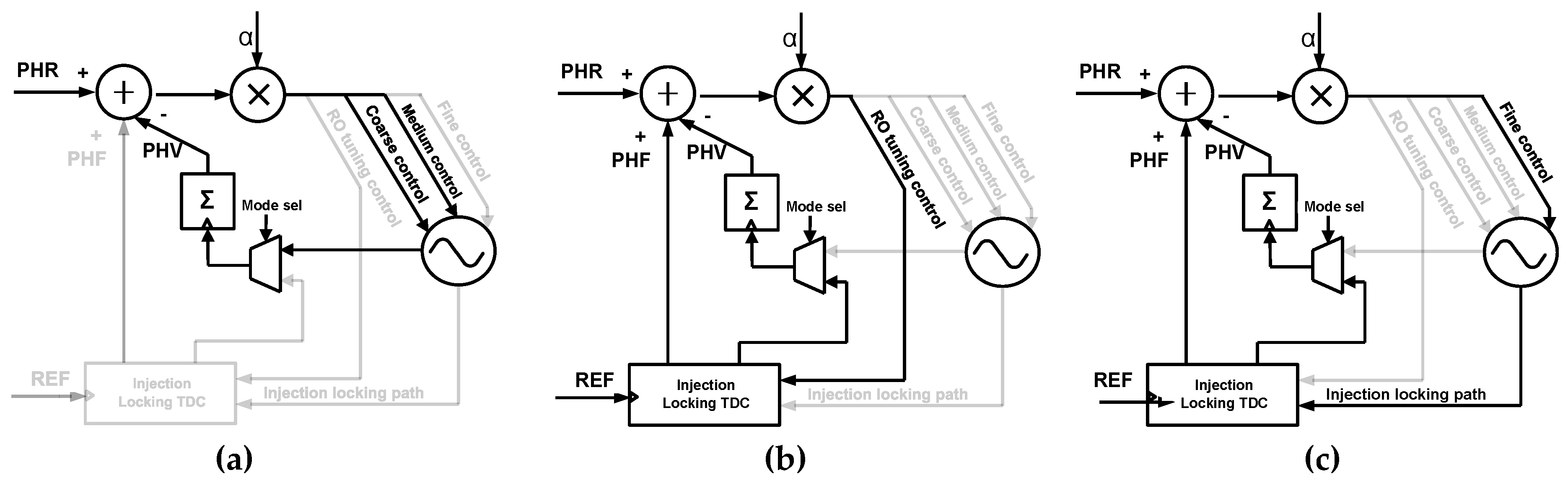
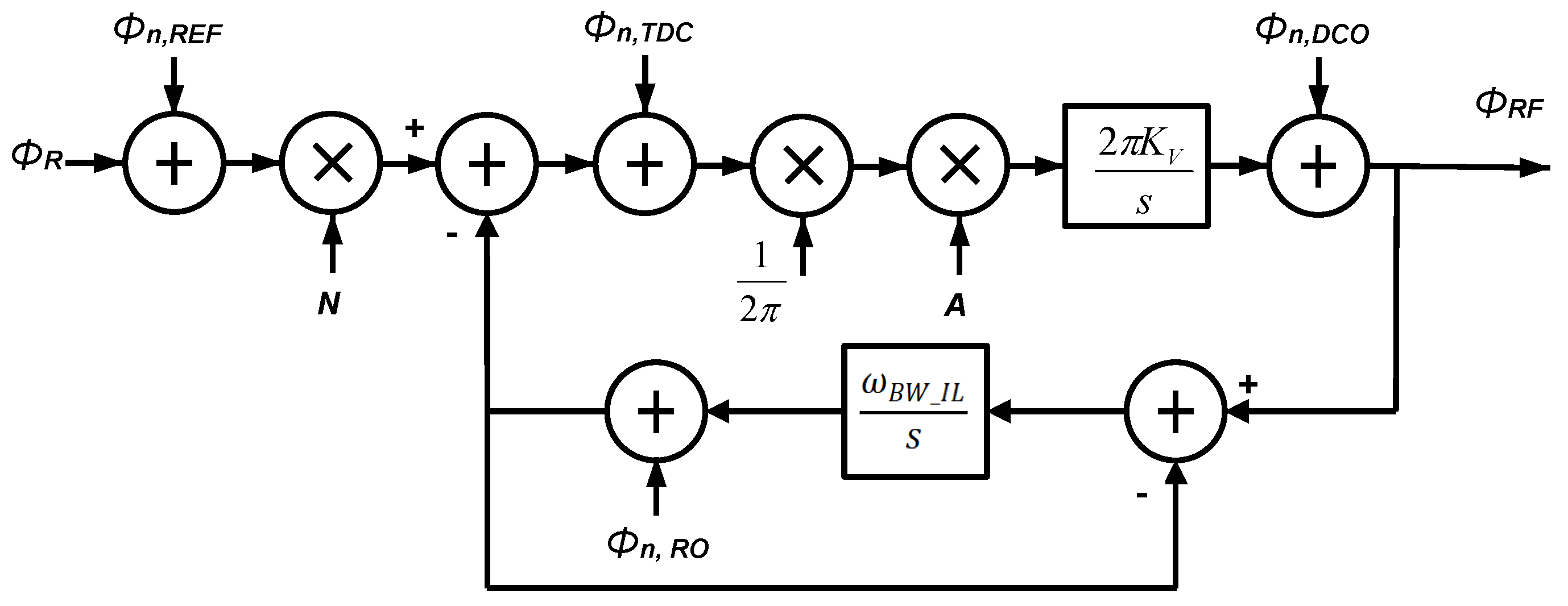
2.3. Proposed ADPLL with Calibration-Free RO-Based Injection Locking TDC

The overall architecture of the proposed type-I ADPLL is shown in Figure 5. To overcome the poor phase noise caused by RO, we use LCDCO to inject the embedded TDC. To achieve a wide output frequency range and high0output frequency accuracy at the same time, LCDCO will adopt three discrete frequency tuning modes: coarse mode, medium mode, and fine mode. The frequency tuning range of each mode will cover the frequency range of at least 6 LSBs of the previous mode. In order to overcome the PVT variations and cover the frequency range of 2.4–2.48 GHz in BLE, the coarse tuning range shall be at least 500 MHz. Based on Equation (8), if we apply N = 6 and ω B W = 500 MHz in this expression, we have I i n j / I O S C = 0.5 ; this will inevitably increase the injection current and power consumption.
Since the coarse mode and medium mode in the ADPLL locking process have no requirements for phase noise, in order to further reduce the power consumption, the improved ADPLL locking process is as follows: When the loop enters the coarse and medium tuning mode, turn off RO and TDC, as shown in the dotted line in Figure 5, we use the output of LCDCO as the input of the high-speed counter, and the loop only calculates the integer part of the phase error. After the medium mode, the frequency accuracy of the target channel will reduce to a few megahertz. Then the RO tuning mode is on, and the output of one phase of RO is used as the input of the counter to calculate the integer phase error. After the coarse RO tuning finishes, the frequency difference between RO and LCDCO is only about 10 MHz, which leaves a small injection-locking bandwidth. Thus, the power consumption of the injection current can be reduced.
After the RO tuning control, the fine control mode is on to complete the final locking, the RO tuning control bits are fixed, and the injection locking path is turned on. Then the fractional phase error is calculated through injection-locked RO-based TDC. Figure 6 shows the functional diagram of different locking modes of the ADPLL.
Since the frequency of free-running RO and the injected source are close enough because of the RO tuning control, according to [22], the transfer function of the injection locking loop can be expressed as:
ϕ out ( s ) ϕ inj ( s ) = H i n j ( s ) = ω B W I L s + ω B W I L .
where ϕ out ( s ) is the injected output phase and ϕ inj ( s ) is the phase of the injection source. From this equation, we can see that the injection locking loop is low pass filtered. Figure 7 shows the phase domain model of the proposed ADPLL with major noise sources, including reference noise, TDC noise, DCO noise, and RO noise.
The open-loop transfer function can be written as:
H o ( s ) = A K v s .
Then the closed-loop transfer function is:
H c ( s ) = N H o ( s ) 1 + H inj ( s ) H o ( s ) = N A K V s + ω B W I L s 2 + s ω B W I L + A K v ω B W I L .
where the damping factor ζ is 0.5 ω B W I L / A K v . The phase noise transfer functions of different noise sources are given by:
ϕ R F ( s ) ϕ n , R O ( s ) = A K v s s 2 + s ω B W I L + A K v ω B W I L ,
ϕ R F ( s ) ϕ n , D C O ( s ) = s 2 + s ω B W I L s 2 + s ω B W I L + A K v ω B W I L ,
ϕ R F ( s ) ϕ n , T D C ( s ) = A K v s + ω B W I L s 2 + s ω B W I L + A K v ω B W I L ,
ϕ R F ( s ) ϕ n , R E F ( s ) = N A K v s + ω B W I L s 2 + s ω B W I L + A K v ω B W I L .
These equations show that the noise contributions are all affected by the injection locking bandwidth ω B W I L . The simulated phase noise of DCO and RO to the ADPLL output with different ω B W I L is shown in Figure 8. It can be seen that with the constant A K v , which determines the loop bandwidth of ADPLL, ω B W I L should not be too small because the loop will become unstable, and the phase noise of ADPLL will get worse by RO. With a proper set of ω B W I L , the noise floor of RO will have no influence on the total PN output.
Figure 9 shows total phase noise with TDC quantization and FREF noise considered. From (20), we can see that the phase noise of FREF will be up-converted by 20 log N . However, because of the superior phase noise performance of the crystal oscillator, the output phase noise will still be below the DCO phase noise. The TDC resolution is equal to a single-stage RO delay t res , which dominates the in-band phase noise of ADPLL. To have a better performance of in-band phase noise, one should increase the number of RO stages so as to decrease t res . However, this will inevitably result in high power consumption.

3. Circuit Implementation

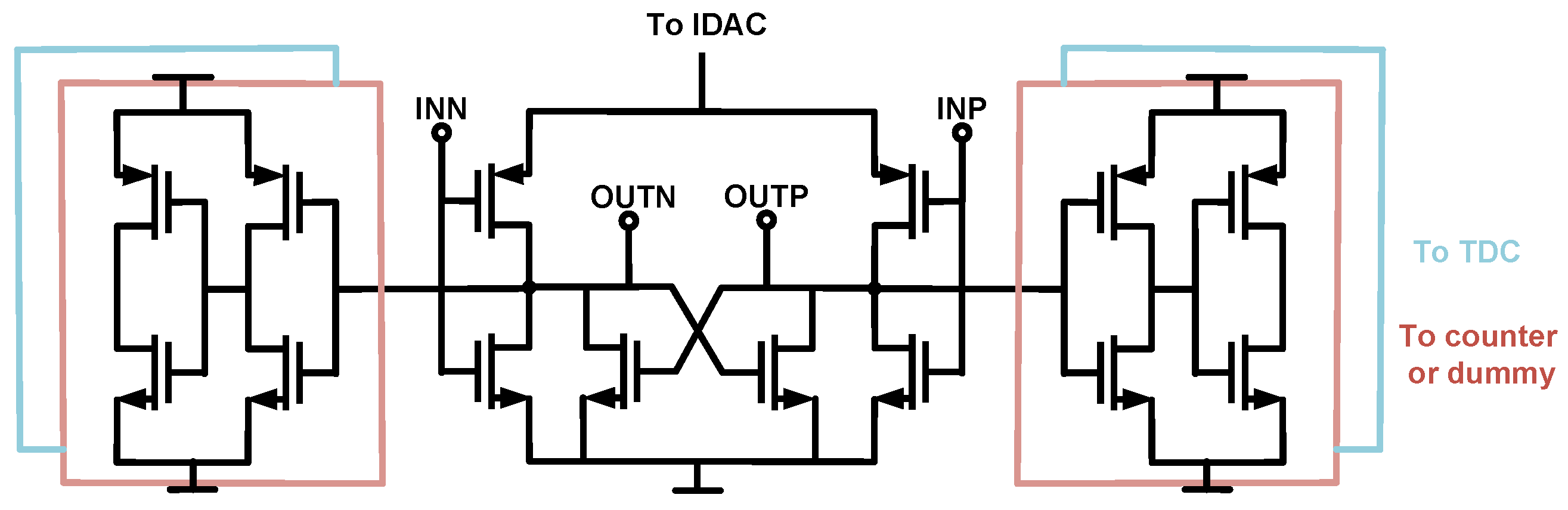
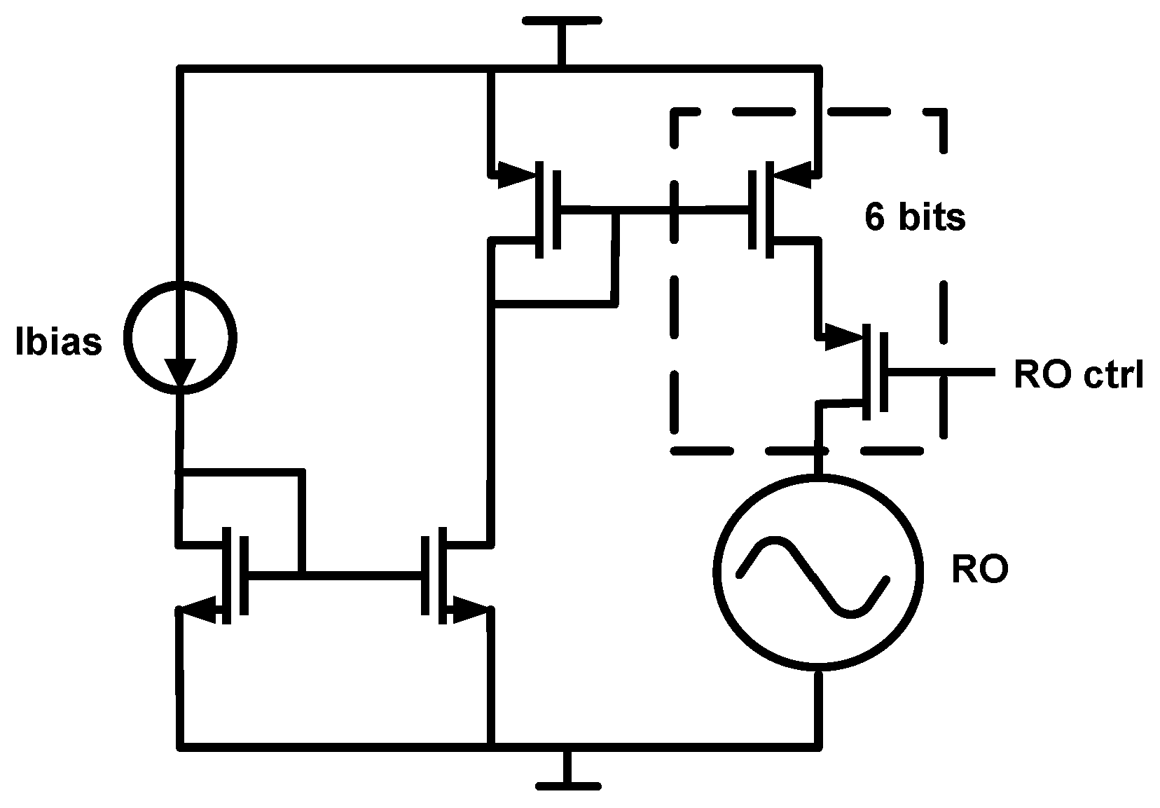
3.1. Ring Oscillator
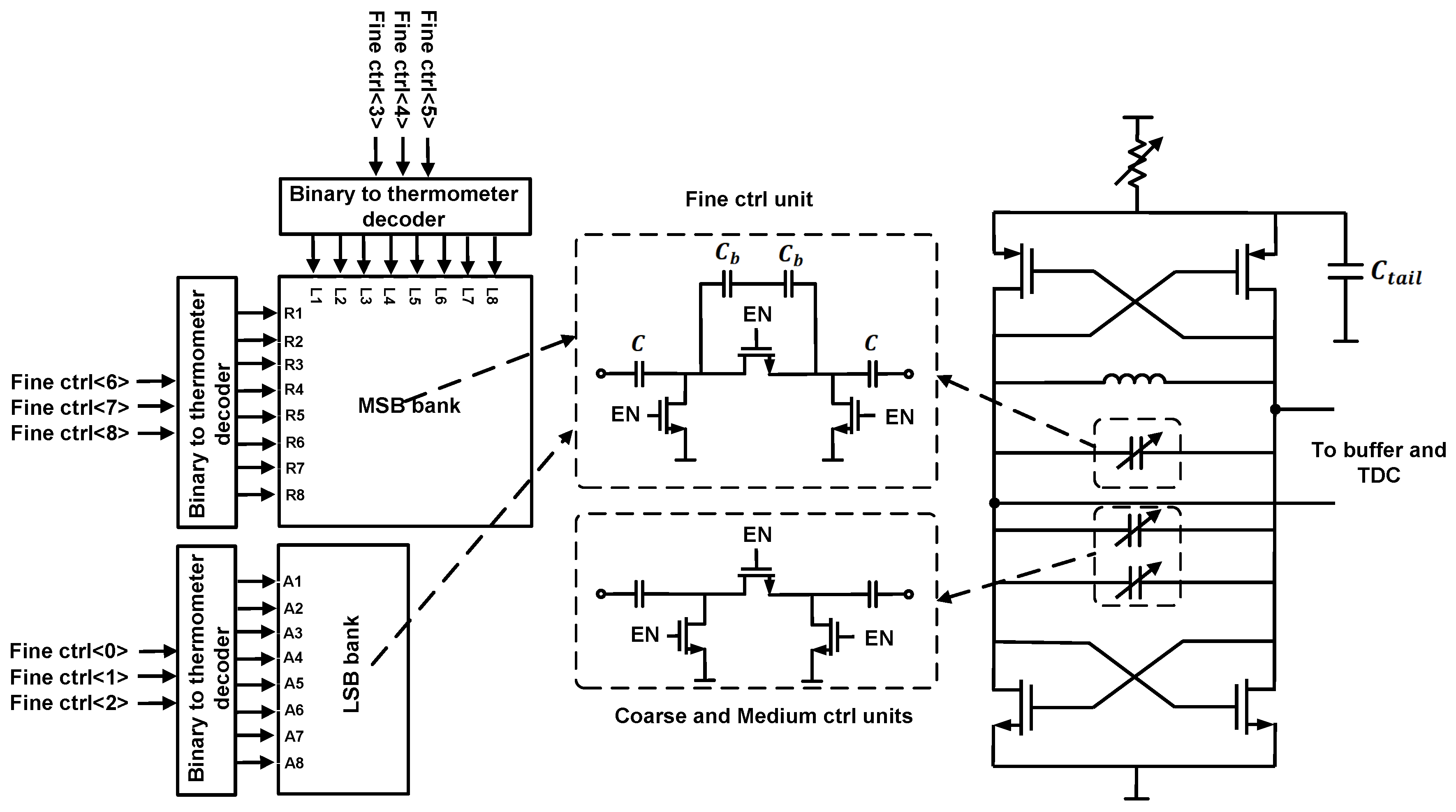
The circuit implementation of injection-locked RO-based TDC is shown in Figure 10. We use a 6-stage pseudo-differential RO to oscillate at 2.4 GHz, which provides 12 TDC phases and t r e s = 34.7 ps . This will result in −91 dBc/Hz in-band phase noise with a 32 MHz reference clock. The output of every phase of RO is connected to the buffer and sampled by FREF. Then the 12 bits output is encoded to roughly 3.5 bits as the fractional phase error of the phase detector. Another output of the RO is also buffered to the counter to accumulate as the integer phase error. To minimize the TDC DNL, every output of RO must connect to two buffers to balance the loading. Therefore, the buffers that are not used are connected to dummies. Since the capacitance loading will decrease the oscillation frequency, one must increase the current to obtain the same frequency. Therefore, the size of the buffer in the first stage is pretty small and increases stage by stage. Similarly, the RO delay cell we choose is two inverter stages with NMOS-only cross-coupled pairs instead of CMOS cross-coupled pairs, as shown in Figure 11. The layout of the RO should also be carefully designed to decrease any unwanted parasitic capacitance.
The oscillation frequency of RO is tuned by the current steering DAC that is shown in Figure 12. The length of these transistors should be wide to implement accurate, current replication. To realize a 10 MHz LSB tuning step of the DAC, we use six control bits to cover at least an 800 MHz tuning range.

3.2. LC-Based DCO

The LCDCO we use is a typical CMOS architecture with both NMOS and PMOS cross-coupled pairs as the negative resistance stage and a digitally tuned resistor tail, as shown in Figure 13. Because of the flicker-noise up-conversion of MOS transistor bias, a poly-silicon resistor is adopted for biasing instead of a MOS-based current source [23]. The resistor only has the thermal noise and will be filtered by the added tail capacitor C t a i l . The current of the LCDCO can be regulated by the resistor, which will result in the variation in output amplitude and phase noise. This bias technique also saves a large amount of area compared to the current source bias.
The power consumption in the LC circuit needs the negative resistance to compensate so as to sustain the oscillation. To find the lower limit of power consumption of the LCDCO, we calculate the energy stored in the capacitor or the inductor that:
W ( t ) = 1 2 L i 2 ( t ) = 1 2 C v 2 ( t ) .
where i ( t ) and v ( t ) are the currents through the inductor and the voltage of the capacitance. Since the quality factor of an on-chip inductor is much worse than the capacitor banks, we make an assumption that the total equivalent parasitic resistance R S is connected in series with the inductors. Combined with (21), the power loss due to R S is equal to:
P loss = 1 2 R s i max 2 = 1 2 C v max 2 R s L .
With the equation f = 1 2 π L C we can conclude that:
P loss = 1 8 π v max 2 R S f 2 L 2 = 1 2 v max 2 L ω Q L .
where Q L is the quality factor of the inductor. We can see from this equation that the power loss is inversely proportional to the inductance if the operating frequency and the equivalent parasitic resistance are constant. However, if the inductance is too large, the tuning range of the capacitor banks will be reduced, and the self-resonant frequency will be decreased. Therefore, in this project, a value of 6.4 nH of inductance is chosen to balance these issues.
The capacitor array of the LC tank in the LCDCO is composed of a coarse capacitor bank, medium capacitor bank, and fine capacitor bank. The control unit of each bank is shown in Figure 13. we use MOM capacitors instead of MOS varactors to realize these three banks because they are less sensitive to PVT variations. In the coarse mode, the unit capacitor of the coarse capacitor bank is set to 25 fF to achieve a 14 MHz tuning step, and we use 6 bits binary control to achieve a 1 GHz tuning range. The control unit of the medium bank is the same as the coarse bank with a difference of a smaller unit capacitor of 3.3 fF to achieve a 2 MHz tuning step, and 6 bits binary control is also adopted to achieve a 120 MHz tuning range. The fine banks are 9 bits that can cover 16 MHz with a tuning step of 40 kHz, which needs a 23 aF capacitor unit. Two capacitors C b with a large C b / C ratio are used to create such a small change of capacitance in fine mode. The fine bank is thermometer-coded to implement an improved matching performance. However, a 9-bit fine bank with the thermometer coded needs 511 unit cells, and the area of each cell is large due to the large C b . To reduce the large area caused by the fine bank, we divide the fine bank into 6 MSB bits and 3 LSB bits, each MSB cell with a step equal to eight times that of the LSB cell. This only produces 63 MSB unit cells and 7 LSB unit cells with a smaller C b in MSB unit cells compared to the LSB unit cells, thus achieving a reduced area and parasites of the fine bank. The diagram of the fine capacitor bank is shown in Figure 13.

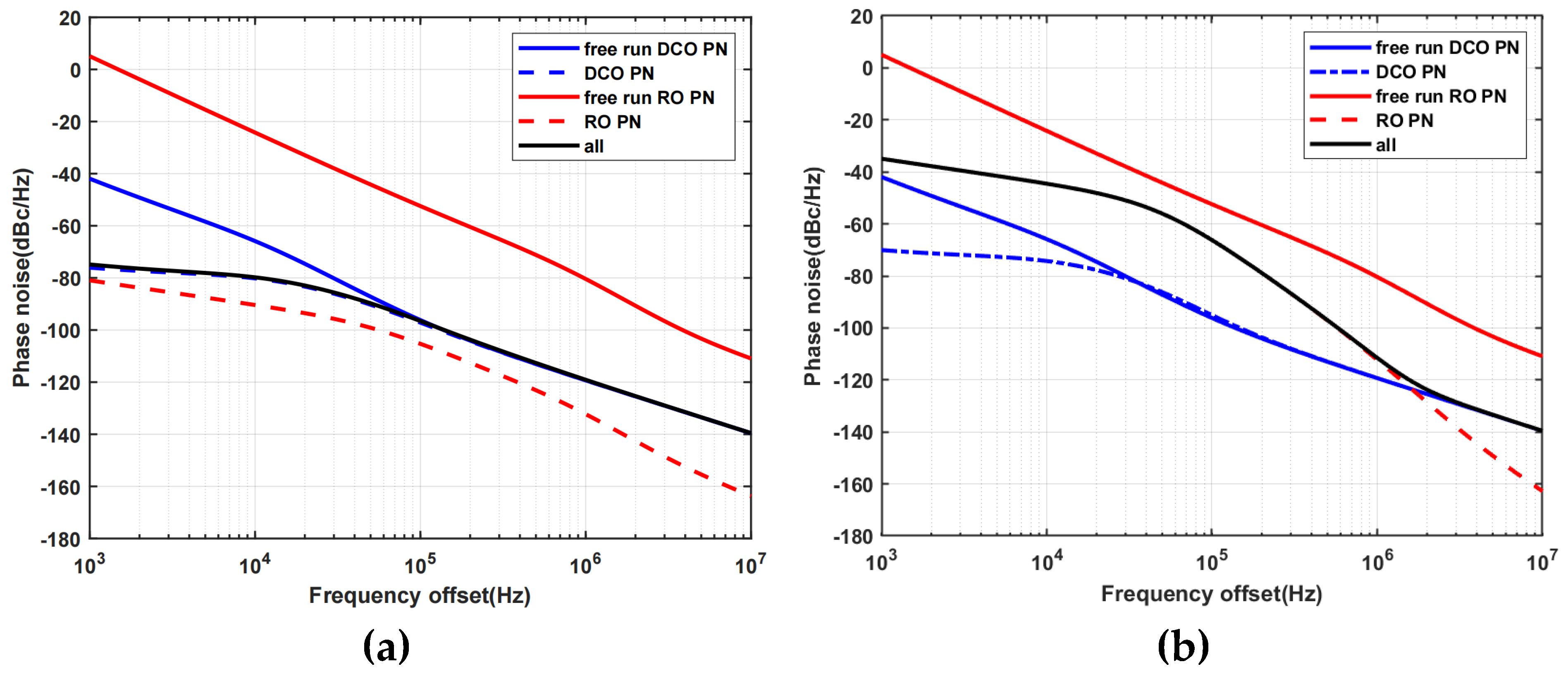
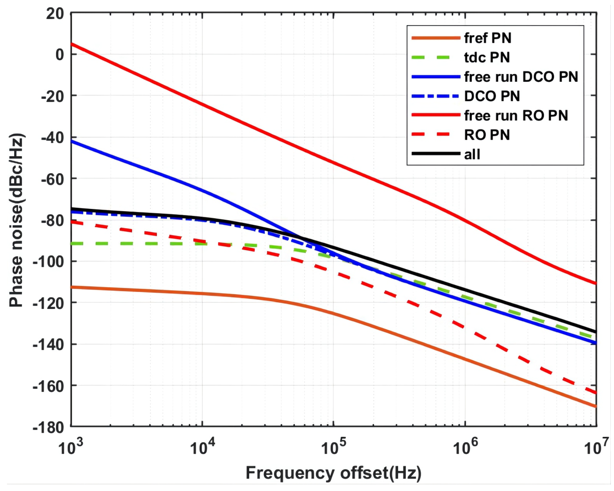
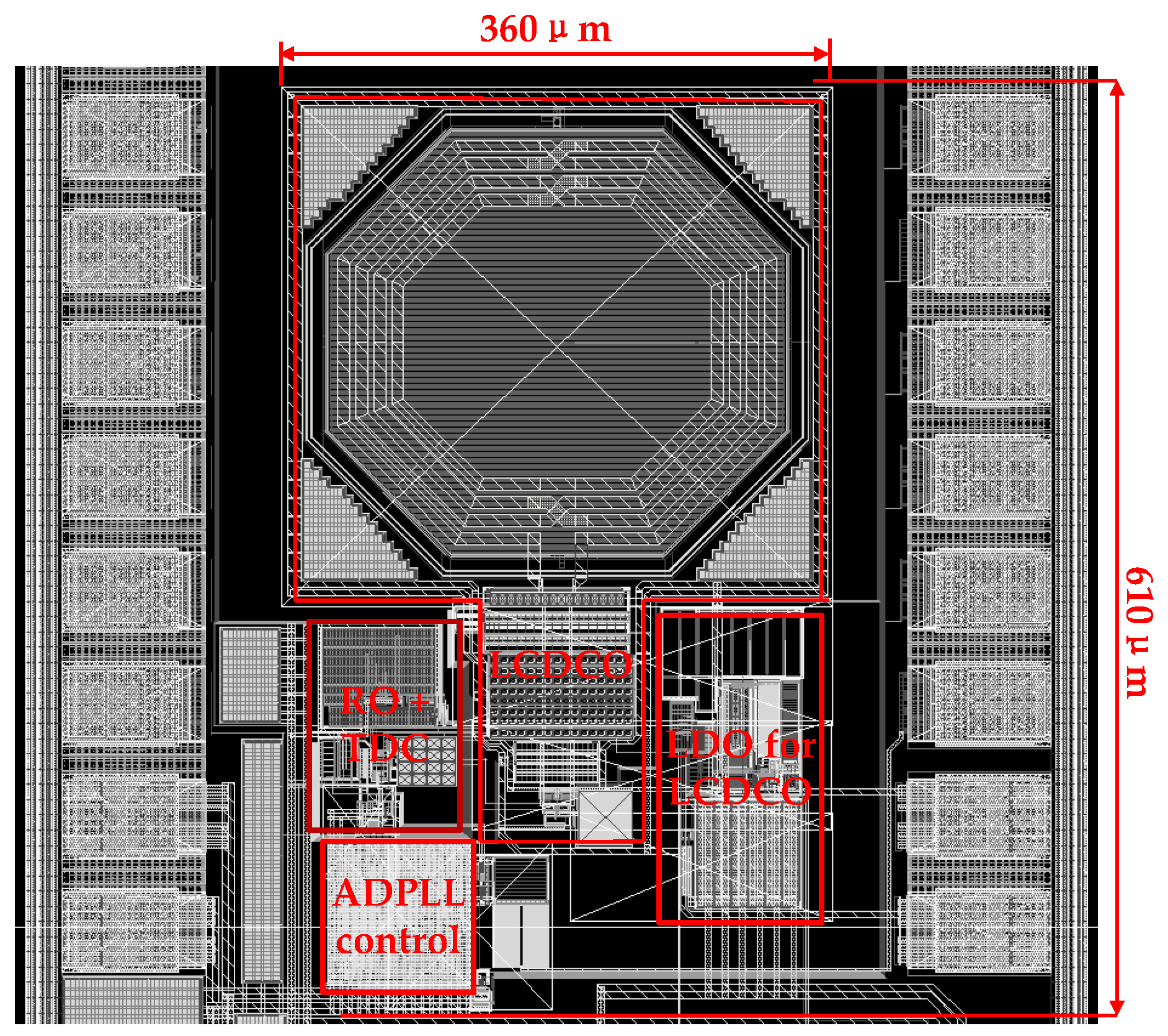
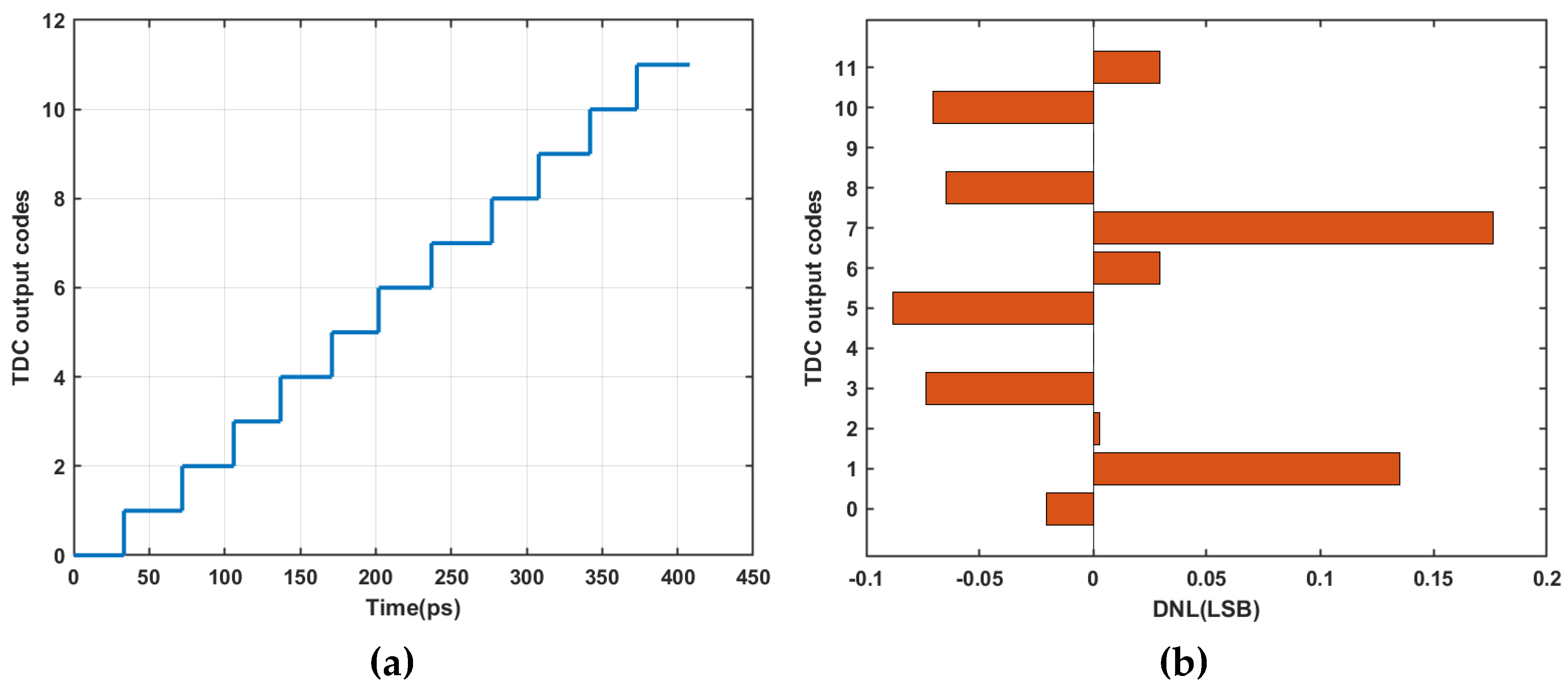
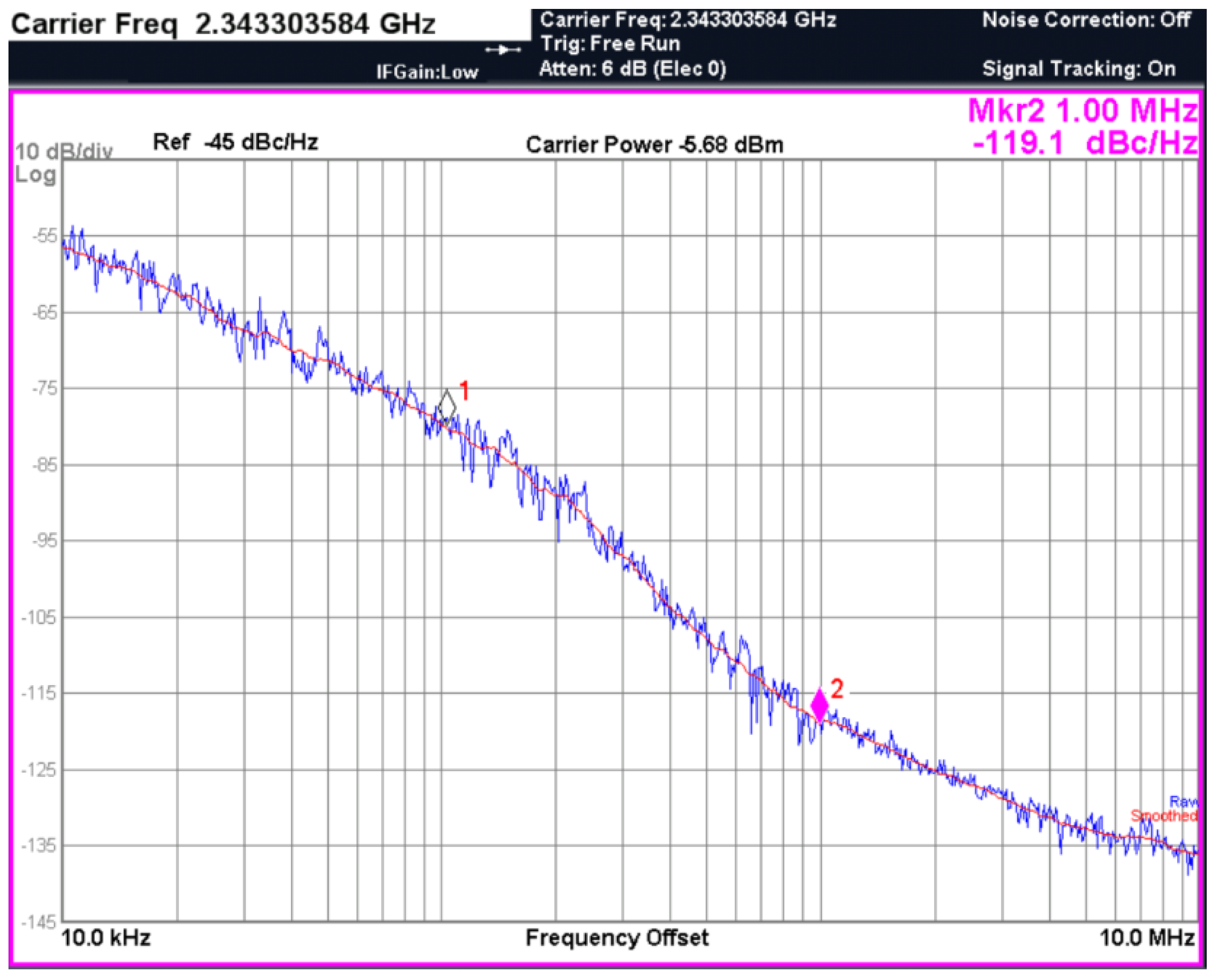
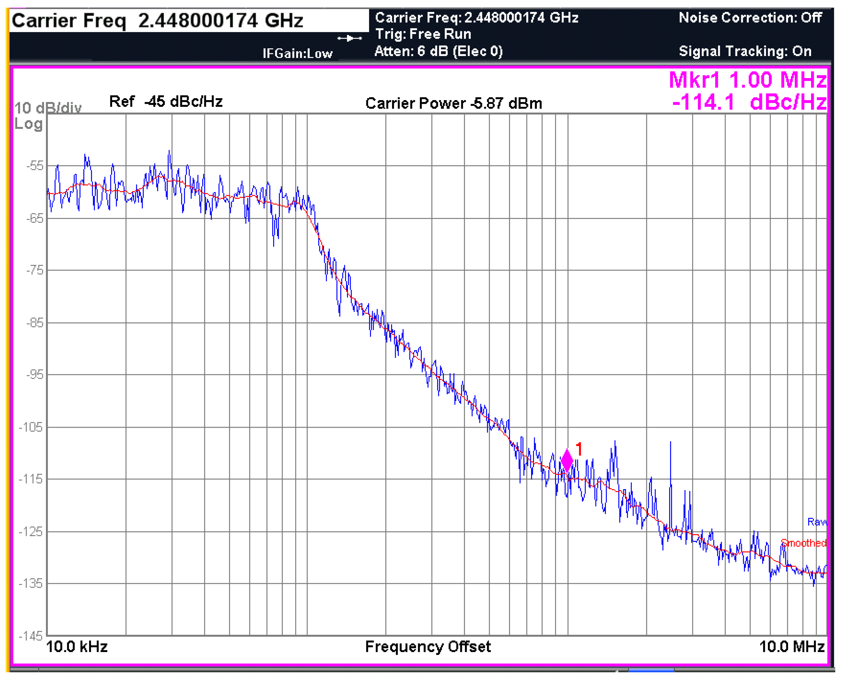
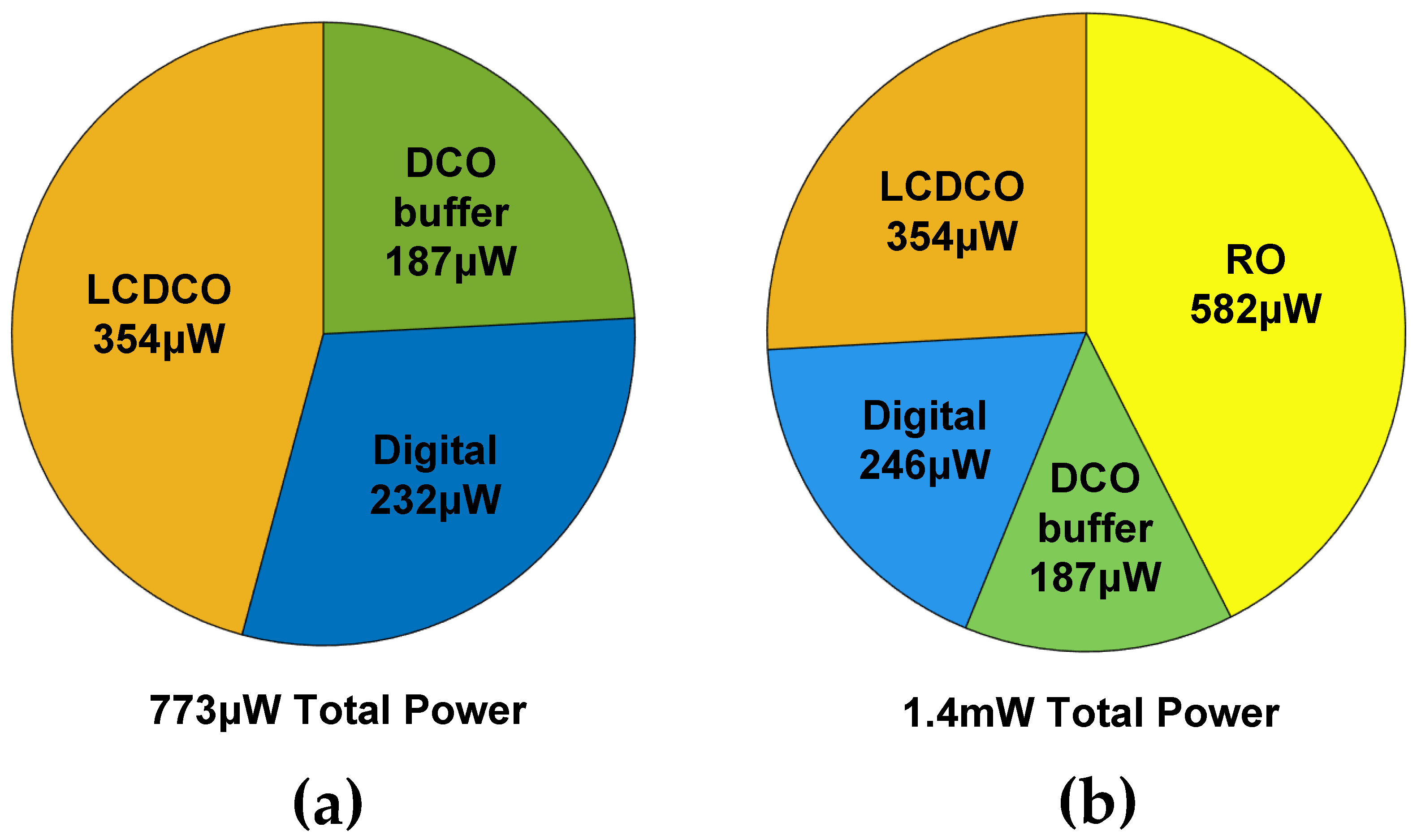
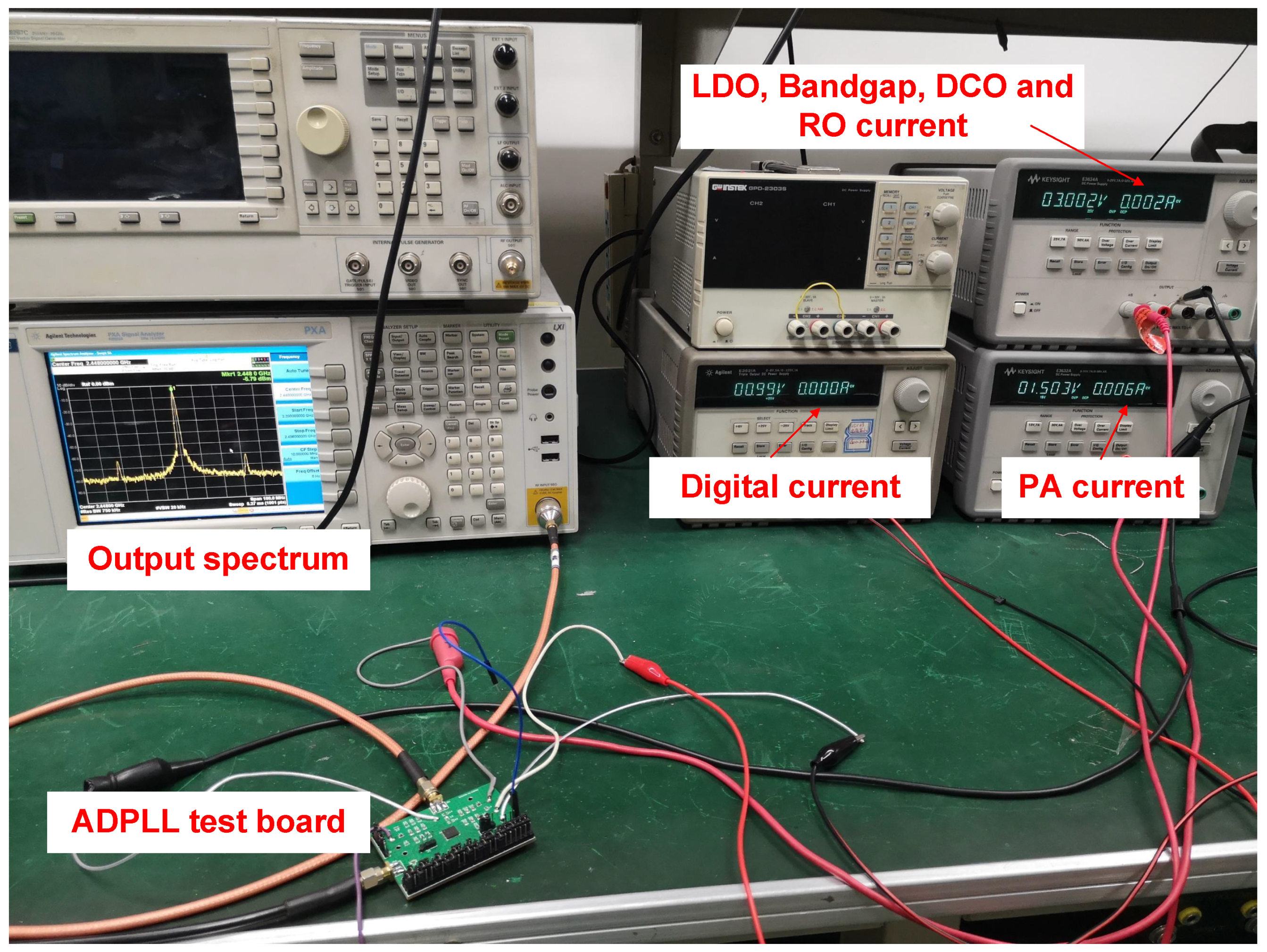
4. Simulation and Measurement Results

The proposed ADPLL was fabricated in a TSMC 40-nm CMOS process, and the layout photograph of the chip is shown in Figure 14. The core area of the ADPLL is 0.22 mm 2 . Figure 15 shows the transient waveform of the ADPLL operation with post-layout simulation. The reference frequency is 32 MHz, and the target frequency is set to 2.414 GHz. The locking process of the ADPLL is divided into the coarse mode, medium mode, RO tuning mode, and fine mode. First, we set the target frequency to 2.414 GHz by manually adjusting the frequency division ratio. Then, the ADPLL works in the coarse mode; the loop is automatically calibrated with a given coarse mode loop bandwidth until the control bits toggle between two adjacent bits. After that, the ADPLL works in the medium mode with the coarse control bits fixed. The medium mode loop bandwidth of ADPLL is set lower compared to the coarse mode to ensure a smaller frequency resolution. After the medium mode, the frequency accuracy of the target frequency will reduce to a few megahertz. Then, the RO is on; the loop waits for 500 ns to make the RO stable. Then the RO tuning mode is on, and the target frequency is also set to 2.414 GHz. At the same time, the LCDCO keeps the tuning bits unchanged. After the RO tuning mode, the switch between the LCDCO and RO is on. The RO is injection-locked by LCDCO in fine mode. The fractional error is calculated by RO-based TDC to complete the final locking. As shown in Figure 15, the ADPLL will toggle between several control bits when the loop is locked. This is caused by the limited quantization error of TDC, and the noise will dominate the in-band phase noise of the ADPLL as the loop bandwidth is wider (e.g., 2 MHz, as shown in Figure 15).
Figure 16 shows the performance of injection-locked TDC after post-layout simulation. The oscillation frequency is set to 2.45 GHz. It can be seen that there are two positive peak values of DNL, which are caused by the differential input of the injection current. However, they are all less than 0.17 LSB, and the influence on ADPLL can be negligible.
To ensure the normal operation of ADPLL, the free oscillation frequency of RO needs to be tuned close to the locking frequency. Figure 17, Figure 18 and Figure 19 shows the measured phase noise performance of the free-running RO, free-running DCO, and the locked ADPLL. We set the target locking frequency to 2.448 GHz. In the RO test mode, the frequency of RO is manually adjusted to the frequency closest to 2.448 GHz. The poor phase noise of RO is shown in Figure 17. We can see that the oscillation frequency of RO is 2.46 GHz, which has a 12 MHz difference compared to the target frequency. Then, the ADPLL skips the RO tuning mode and finally locks to 2.448 GHz. The loop bandwidth is set to 100 kHz to reduce the in-band phase noise of TDC. The phase noise performance of the closed-loop is shown in Figure 19, which is the same when the RO is set to auto-tuning mode, showing that with a proper setting, the phase noise of RO will not influence the total phase noise of ADPLL. The ADPLL spectrum output is shown in Figure 20, and the reference spur is −65 dBc.
The measured power consumption of the ADPLL with a 1 V power supply is shown in Figure 21. In coarse mode and medium mode, the RO is shut down, and the total power consumption is only 773 μ W . In RO tuning mode and fine mode, the LCDCO and buffer consume 541 μ W , and the RO and digital part consume 582 μ W and 246 μ W . The total power of ADPLL consumes 1.4 mW. Figure 22 shows the test environment. The external power supply consists of three separate parts. The digital part of the circuit is directly powered by an external 1 V supply, and the PA is a 1.5 V supply. To ensure the best performance of the oscillator, the power supply of LCDCO and the RO are separated by two low-dropout (LDO) regulators. The LDO is powered by a 3 V supply, and the total current consumption is 2 mA, including the internal bandgap circuit. Table 1 shows the ADPLL performance compared with the state-of-the-art. The power consumption of the proposed work is only 1.4 mW, which is comparable with the advanced low-power ADPLL designs but with a better out-of-band phase noise [12,24]. The ADPLL of [15] consumes only 379 μ W because of the ultra-low-power RO and reduced locking frequency. However, the much worse phase noise performance lowers the PLL FoM. The balanced performance of our work will be more attractive in a BLE transceiver design.

5. Conclusions

In this paper, a low-power ADPLL with calibration-free RO-based injection-locking TDC is proposed. By analyzing the injection-locking behavior and its influence on phase noise and the TDC performance, we use six pseudo-differential stages RO as 3.5 bits TDC to balance the in-band phase noise and the power consumption. The injection-locking bandwidth is set to 10 MHz to minimize the injection current. The ADPLL is divided into four modes, and the fractional phase detection of the phase error is turned down to reduce power. The LCDCO is used to inject the RO-based TDC and consumes only 354 μ W. The total power of 1.4 mW is achieved when the ADPLL is locked. Moreover, it can further benefit from technology scaling due to its digitally intensive nature.

Author Contributions

Conceptualization, Q.C.; methodology, Q.C., Q.S. and S.H.; software, Q.C., Q.S. and Z.W.; validation, Q.C., Q.S. and Z.W.; formal analysis, Q.C.; investigation, Q.C.; resources, Q.C.; writing—original draft preparation, Q.C.; writing—review and editing, Q.C., X.W., S.H. and Y.L.; project administration, X.W., S.H. and Y.L. All authors have read and agreed to the published version of the manuscript.

Funding

This work was supported by the National Key Research and Development Program of China under Grant No.2019YFB2204500.

Conflicts of Interest

The authors declare no conflict of interest.

References

  1. Ryu, D.S.; Yeon, Y.M.; Kim, S.H. Multilink Internet-of-Things Sensor Communication Based on Bluetooth Low Energy Considering Scalability. Electronics 2021, 10, 2335. [Google Scholar] [CrossRef]
  2. Ruiz, L.J.L.; Ridder, M.; Fan, D.; Gong, J.; Li, B.M.; Mills, A.C.; Cobarrubias, E.; Strohmaier, J.; Jur, J.S.; Lach, J. Self-Powered Cardiac Monitoring: Maintaining Vigilance with Multi-Modal Harvesting and E-Textiles. IEEE Sens. J. 2021, 21, 2263–2276. [Google Scholar] [CrossRef]
  3. Li, S.; Breiholz, J.; Kamineni, S.; Im, J.; Wentzloff, D.D.; Calhoun, B.H. An 85 nW IoT Node-Controlling SoC for MELs Power-Mode Management and Phantom Energy Reduction. In Proceedings of the 2020 IEEE International Symposium on Circuits and Systems (ISCAS), Sevilla, Spain, 10–21 October 2020; pp. 1–5. [Google Scholar] [CrossRef]
  4. García-Ortiz, J.C.; Silvestre-Blanes, J.; Sempere-Payá, V. Experimental Application of Bluetooth Low Energy Connectionless in Smart Cities. Electronics 2021, 10, 2735. [Google Scholar] [CrossRef]
  5. Bechthum, E.; Dijkhuis, J.; Ding, M.; He, Y.; Van Den Heuvel, J.; Mateman, P.; Van Schaik, G.J.; Shibata, K.; Song, M.; Tiurin, E.; et al. 30.6 A Low-Power BLE Transceiver with Support for Phase-Based Ranging, Featuring 5 µs PLL Locking Time and 5.3 ms Ranging Time, Enabled by Staircase-Chirp PLL with Sticky-Lock Channel-Switching. In Proceedings of the 2020 IEEE International Solid-State Circuits Conference, San Francisco, CA, USA, 16–20 February 2020; pp. 470–472. [Google Scholar] [CrossRef]
  6. Yahya, F.; Lukas, C.J.; Breiholz, J.; Roy, A.; Patel, H.N.; Liu, N.; Chen, X.; Kosari, A.; Li, S.; Akella, D.; et al. A battery-less 507 nW SoC with integrated platform power manager and SiP interfaces. In Proceedings of the 2017 Symposium on VLSI Circuits, Kyoto, Japan, 5–8 June 2017; pp. C338–C339. [Google Scholar] [CrossRef]
  7. Staszewski, R.; Wallberg, J.; Rezeq, S.; Hung, C.M.; Eliezer, O.; Vemulapalli, S.; Fernando, C.; Maggio, K.; Staszewski, R.; Barton, N.; et al. All-digital PLL and transmitter for mobile phones. IEEE J. Solid-State Circuits 2005, 40, 2469–2482. [Google Scholar] [CrossRef]
  8. Staszewski, R.; Muhammad, K.; Leipold, D.; Hung, C.M.; Ho, Y.C.; Wallberg, J.; Fernando, C.; Maggio, K.; Staszewski, R.; Jung, T.; et al. All-digital TX frequency synthesizer and discrete-time receiver for Bluetooth radio in 130-nm CMOS. IEEE J. Solid-State Circuits 2004, 39, 2278–2291. [Google Scholar] [CrossRef]
  9. Lin, J.M.; Yang, C.Y. A Fast-Locking All-Digital Phase-Locked Loop with Dynamic Loop Bandwidth Adjustment. IEEE Trans. Circuits Syst. I Regul. Pap. 2015, 62, 2411–2422. [Google Scholar] [CrossRef]
  10. Hsu, C.M.; Straayer, M.Z.; Perrott, M.H. A Low-Noise Wide-BW 3.6-GHz Digital ΔΣ Fractional-N Frequency Synthesizer with a Noise-Shaping Time-to-Digital Converter and Quantization Noise Cancellation. IEEE J. Solid-State Circuits 2008, 43, 2776–2786. [Google Scholar] [CrossRef]
  11. Elkholy, A.; Anand, T.; Choi, W.S.; Elshazly, A.; Hanumolu, P.K. A 3.7 mW Low-Noise Wide-Bandwidth 4.5 GHz Digital Fractional-N PLL Using Time Amplifier-Based TDC. IEEE J. Solid-State Circuits 2015, 50, 867–881. [Google Scholar] [CrossRef]
  12. Tamura, M.; Takano, H.; Nakahara, H.; Fujita, H.; Arisaka, N.; Shinke, S.; Suzuki, N.; Nakada, Y.; Shinohe, Y.; Etou, S.; et al. A 0.5-V BLE Transceiver with a 1.9-mW RX Achieving -96.4-dBm Sensitivity and -27-dBm Tolerance for Intermodulation From Interferers at 6- and 12- MHz Offsets. IEEE J. Solid-State Circuits 2020, 55, 3376–3386. [Google Scholar] [CrossRef]
  13. Ho, C.R.; Chen, M.S.W. A Fractional-N DPLL with Calibration-Free Multi-Phase Injection-Locked TDC and Adaptive Single-Tone Spur Cancellation Scheme. IEEE Trans. Circuits Syst. I Regul. Pap. 2016, 63, 1111–1122. [Google Scholar] [CrossRef]
  14. Chillara, V.K.; Liu, Y.H.; Wang, B.; Ba, A.; Vidojkovic, M.; Philips, K.; de Groot, H.; Staszewski, R.B. 9.8 An 860 μW 2.1-to-2.7 GHz all-digital PLL-based frequency modulator with a DTC-assisted snapshot TDC for WPAN (Bluetooth Smart and ZigBee) applications. In Proceedings of the 2014 IEEE International Solid-State Circuits Conference Digest of Technical Papers (ISSCC), San Francisco, CA, USA, 9–13 February 2014; pp. 172–173. [Google Scholar] [CrossRef]
  15. Chen, X.; Breiholz, J.; Yahya, F.B.; Lukas, C.J.; Kim, H.S.; Calhoun, B.H.; Wentzloff, D.D. Analysis and Design of an Ultra-Low-Power Bluetooth Low-Energy Transmitter with Ring Oscillator-Based ADPLL and 4 × Frequency Edge Combiner. IEEE J. Solid-State Circuits 2019, 54, 1339–1350. [Google Scholar] [CrossRef]
  16. Kuo, F.W.; Binsfeld Ferreira, S.; Chen, H.N.R.; Cho, L.C.; Jou, C.P.; Hsueh, F.L.; Madadi, I.; Tohidian, M.; Shahmohammadi, M.; Babaie, M.; et al. A Bluetooth Low-Energy Transceiver with 3.7-mW All-Digital Transmitter, 2.75-mW High-IF Discrete-Time Receiver, and TX/RX Switchable On-Chip Matching Network. IEEE J. Solid-State Circuits 2017, 52, 1144–1162. [Google Scholar] [CrossRef] [Green Version]
  17. Chen, M.S.W.; Su, D.; Mehta, S. A Calibration-Free 800 MHz Fractional-N Digital PLL with Embedded TDC. IEEE J. Solid-State Circuits 2010, 45, 2819–2827. [Google Scholar] [CrossRef]
  18. Yoo, S.; Choi, S.; Lee, Y.; Seong, T.; Lim, Y.; Choi, J. A Low-Jitter and Low-Reference-Spur Ring-VCO- Based Injection-Locked Clock Multiplier Using a Triple-Point Background Calibrator. IEEE J. Solid-State Circuits 2021, 56, 298–309. [Google Scholar] [CrossRef]
  19. Razavi, B. A study of injection locking and pulling in oscillators. IEEE J. Solid-State Circuits 2004, 39, 1415–1424. [Google Scholar] [CrossRef]
  20. Pandey, J.; Otis, B.P. A Sub-100 μW MICS/ISM Band Transmitter Based on Injection-Locking and Frequency Multiplication. IEEE J. Solid-State Circuits 2011, 46, 1049–1058. [Google Scholar] [CrossRef]
  21. Lin, C.C.; Hu, H.; Gupta, S. Spur Minimization Techniques for Ultra-Low-Power Injection-Locked Transmitters. IEEE Trans. Circuits Syst. I Regul. Pap. 2020, 67, 3643–3655. [Google Scholar] [CrossRef]
  22. Adler, R. A Study of Locking Phenomena in Oscillators. Proc. IRE 1946, 34, 351–357. [Google Scholar] [CrossRef]
  23. Hegazi, E.; Sjoland, H.; Abidi, A. A filtering technique to lower LC oscillator phase noise. IEEE J. Solid-State Circuits 2001, 36, 1921–1930. [Google Scholar] [CrossRef] [Green Version]
  24. Liu, Y.H.; Van Den Heuvel, J.; Kuramochi, T.; Busze, B.; Mateman, P.; Chillara, V.K.; Wang, B.; Staszewski, R.B.; Philips, K. An Ultra-Low Power 1.7–2.7 GHz Fractional-N Sub-Sampling Digital Frequency Synthesizer and Modulator for IoT Applications in 40 nm CMOS. IEEE Trans. Circuits Syst. I Regul. Pap. 2017, 64, 1094–1105. [Google Scholar] [CrossRef]
Figure 1. (a) Divider-based ADPLL; (b) Counter-based ADPLL; (c) Counter-based ADPLL with embed TDC; (d) Counter-based ADPLL with injection-locked RO based TDC.
Electronics 11 01953 g001
Figure 2. (a) N-stage single-end ring oscillator; (b) Current vector diagram.
Electronics 11 01953 g002
Figure 3. (a) N-stage single-end ring oscillator under injection locking; (b) Current vector diagram under injection locking; (c) Current vector diagram of the boundary of injection locking with given strength of the injection current.
Electronics 11 01953 g003
Figure 4. (a) Classical Flash TDC; (b) Embedded TDC.
Electronics 11 01953 g004
Figure 5. Block diagram of the proposed ADPLL.
Electronics 11 01953 g005
Figure 6. (a) Coarse mode and medium mode of the proposed ADPLL; (b) RO tuning mode of the proposed ADPLL; (c) Fine mode of the proposed ADPLL.
Electronics 11 01953 g006
Figure 7. Noise model of the proposed ADPLL.
Electronics 11 01953 g007
Figure 8. ADPLL phase noise contributed by DCO and RO with A K v = 160 kHz . (a) ω B W I L = 20 MHz ; (b) ω B W I L = 100 kHz .
Electronics 11 01953 g008
Figure 9. Total phase noise contribution of the proposed ADPLL.
Electronics 11 01953 g009
Figure 10. Circuit implementation of the injection-locked RO-based TDC.
Electronics 11 01953 g010
Figure 11. Circuit of the RO delay cell.
Electronics 11 01953 g011
Figure 12. Circuit of the current steering DAC.
Electronics 11 01953 g012
Figure 13. Circuit of the LCDCO.
Electronics 11 01953 g013
Figure 14. Layout photograph of the ADPLL chip.
Electronics 11 01953 g014
Figure 15. Transient waveform of the system operation with post-layout simulation.
Electronics 11 01953 g015
Figure 16. (a) TDC gain with post-layout simulation; (b)DNL performance of TDC.
Electronics 11 01953 g016
Figure 17. Measured phase noise performance of free-running RO.
Electronics 11 01953 g017
Figure 18. Measured phase noise performance of free-running DCO.
Electronics 11 01953 g018
Figure 19. Measured phase noise performance of closed-loop ADPLL.
Electronics 11 01953 g019
Figure 20. Measured ADPLL spurious performance.
Electronics 11 01953 g020
Figure 21. ADPLL power breakdown in (a) coarse mode, medium mode, and (b) RO tuning mode and fine mode.
Electronics 11 01953 g021
Figure 22. ADPLL test environment.
Electronics 11 01953 g022
Table 1. Performance comparison with the state-of-the-art.
TCAS-I 2016 [13]JSSC 2019 [15]TCAS-I 2017 [24]JSSC 2020 [12]This Work
Technology65 nm CMOS40 nm CMOS40 nm CMOS22 nm FD-SOI40 nm CMOS
Frequency Range2.7–4.8 G2.4–2.48 G1.7–2.7 G2.4–2.48 G2.4–2.48 G
PLL ArchitectureLCDCO + Injection-
locked
RO
RO-basedLCDCO + Snapshot
DTC-based
TDC
LCDCO + SAR-
ADC-based
TDC
LCDCO + Injection-
locked
RO
Phase Noise−90 dBc/Hz
@40 kHz
−128 dBc/Hz
@3 MHz
−85 dBc/Hz
@1 MHz
−109 dBc/Hz
@1 MHz
−85 dBc/Hz
@10 kHz
−110 dBc/Hz
@1 MHz
−114 dBc/Hz
@1 MHz
Power
Consumption
21.2 mW379  μ W1.19 mW1.25 mW1.4 mW
PLL FoM 1N/A−208.5−234.6N/A−212.1
1 FoM = 10 log10 (( σ jitter 2 ) ∗ ( P 1 m W )).
Publisher’s Note: MDPI stays neutral with regard to jurisdictional claims in published maps and institutional affiliations.

