
Design and Optimization of Miniaturized Microstrip Patch Antennas Using a Genetic Algorithm

 , ,
, , 
Abstract
:1. Introduction
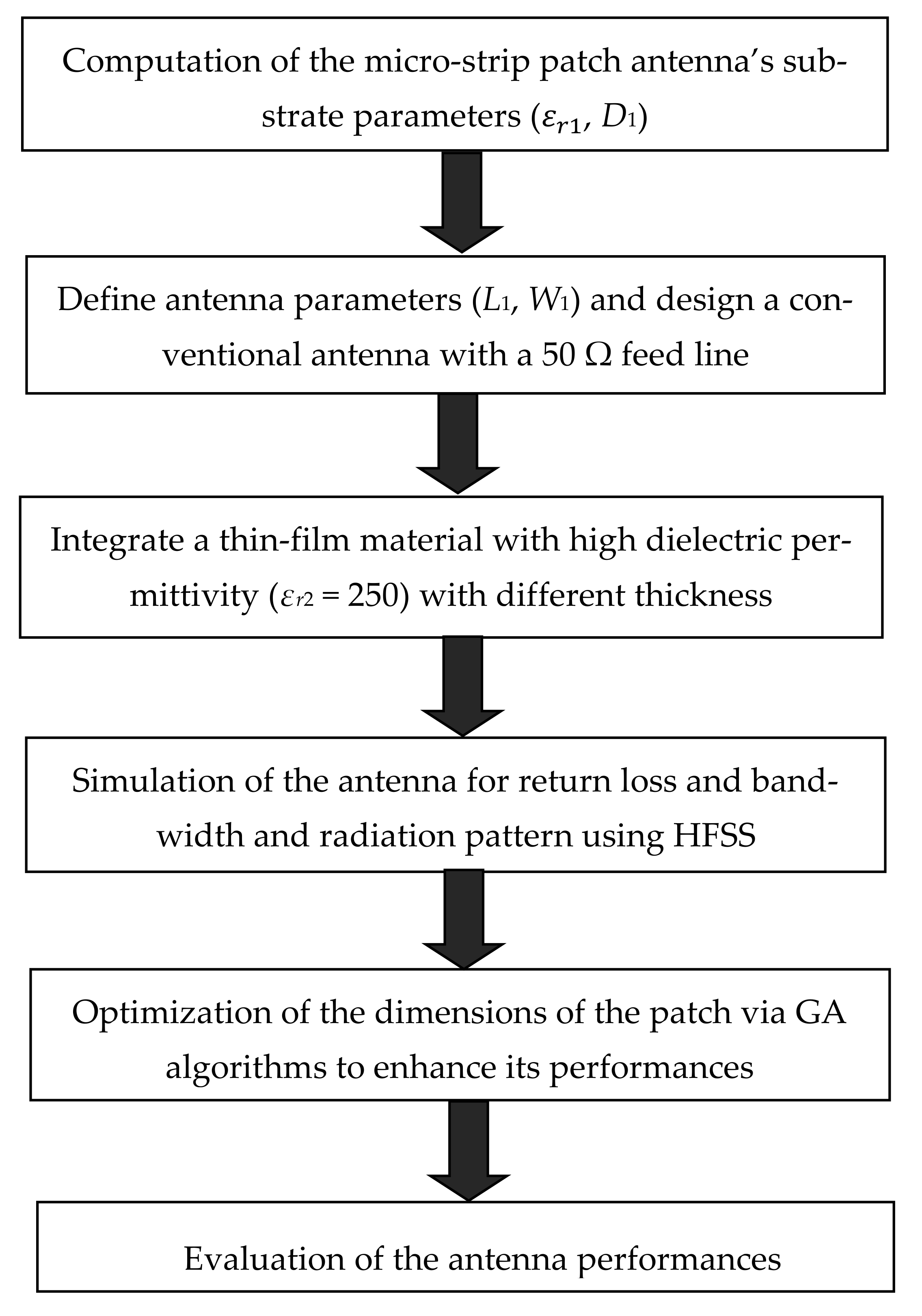
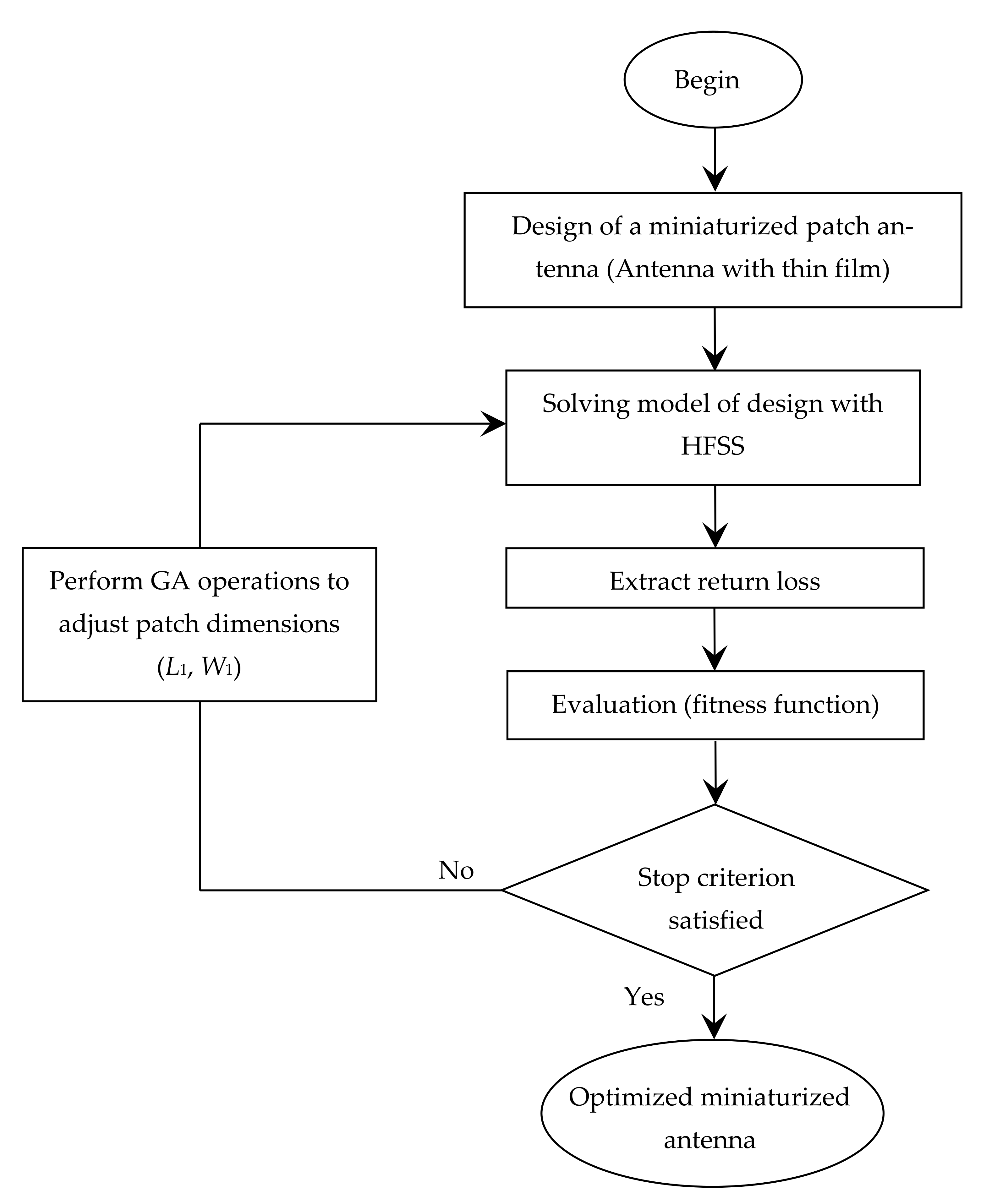
2. Methodology
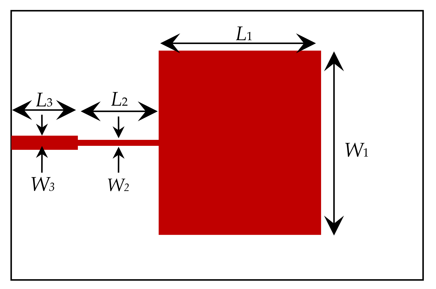
2.1. Initial Geometry of the Antenna
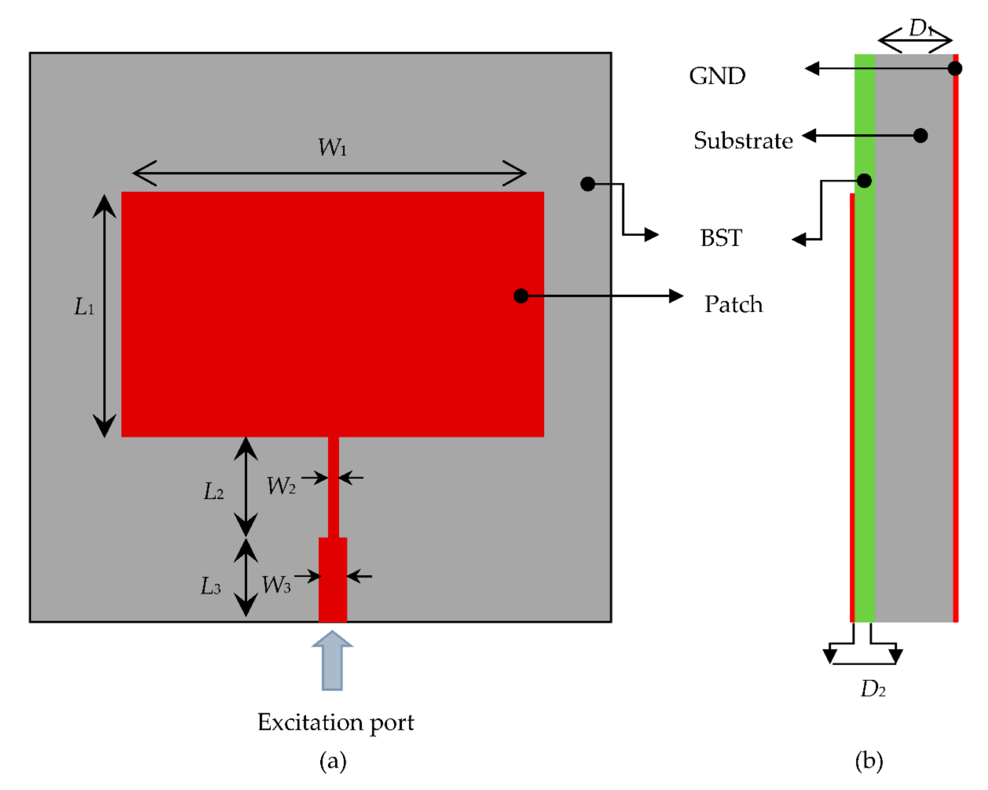
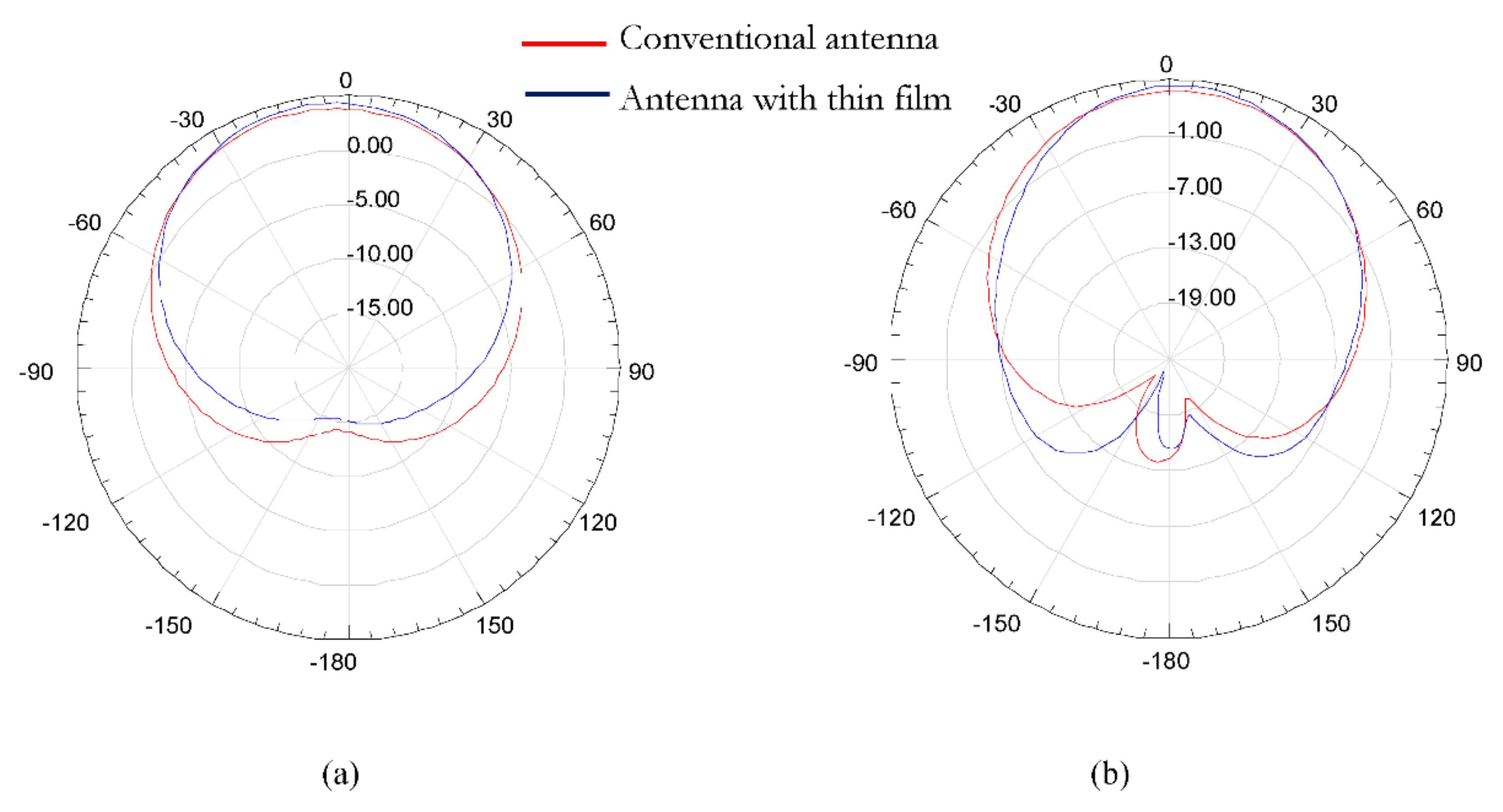
2.2. Antenna with the Thin-Film Material
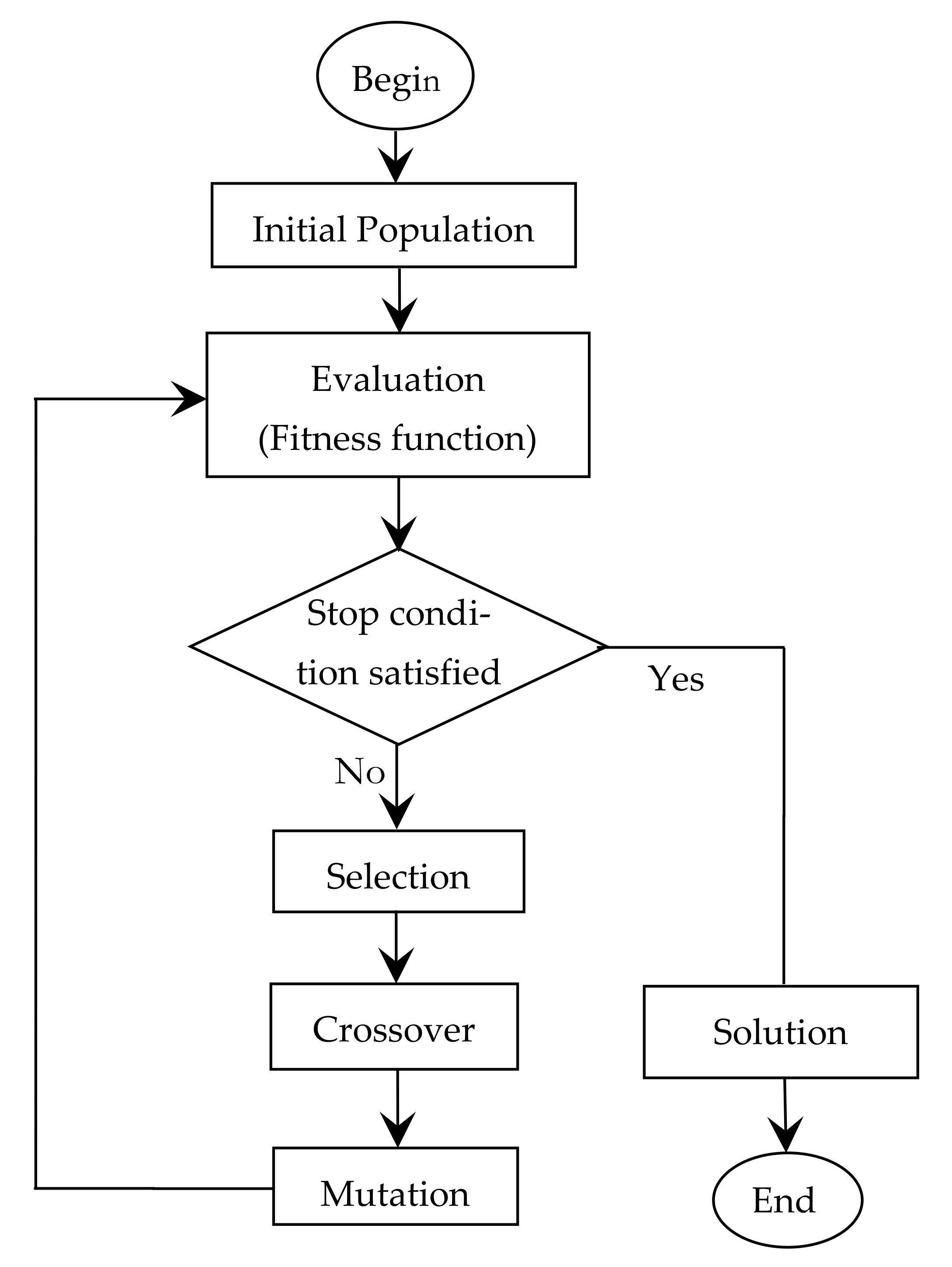
2.3. GA-Based Optimization of the Patch Parameters of the Antenna with the Thin-Film Material
- -
- Optimization is possible for continuous or discrete variables,
- -
- Ability to work with a large number of variables,
- -
- It is well suited to parallel computers.
- -
- It works with numerically generated data, experimental data, or analytical functions.
- Generation of the initial population: A binary string is used to represent all chromosomes, to exemplify chromosome X: 11110000 and chromosome Y: 11001100.
- The initial population is produced via a mechanism capable of creating a non-homogeneous population of individuals that will serve as a basis for future generations. Population size and the total number of individuals directly influence the convergence of the GA. Because the goal is the identification of the optimal values of L1 and W1, the population size is set to 30 and the number of individuals is set to 2.
- Selection: The fitness function is used to evaluate and classify populations. For the next generation, populations offering the best fitness rates will be selected.
- Crossover: from parents, genes are recombined to form a novel chromosome; chromosome X: 11110000 and Chromosome Y: 11001100 might be crossed over after the fourth locus to form two new offspring chromosomes, 11111100 and 11000000. With a constant probability (CP), the crossover is applied to the population. Usually, this constant relies on the application and it is very large [48]. In this work, CP has been set to 0.9.
- Mutation: for producing novel offspring, a few chromosome bits are changed. In binary encoding, some randomly selected bits may be modified from 1 to 0 or vice versa, for example, chromosome 11110110 can possibility be changed in the third location to produce chromosome 11110010. In general, in this operator, it is suitable to choose a low probability of mutation (MP). Typically, MP ranges from 0.01 to 0.3. [48,49]. In this work, MP is equal to 0.05.
- Evaluation Function: for any optimization method, the evaluation function is the most important stage in the optimization procedure’s success. Moreover, it presents the relation between the physical problem to be optimized and the GA. The best solution is one, which diminishes the fitness function (σ). The aim of the study is the minimization of the maximum return loss magnitude (S11) at three frequencies, f1 = 3.8 GHz, fr = 4.0 GHz, and f2 = 4.2 GHz (to widen the bandwidth while keeping the resonance frequency at 4 GHz). In this case, σ is defined as [50]:
3. Results and Discussion
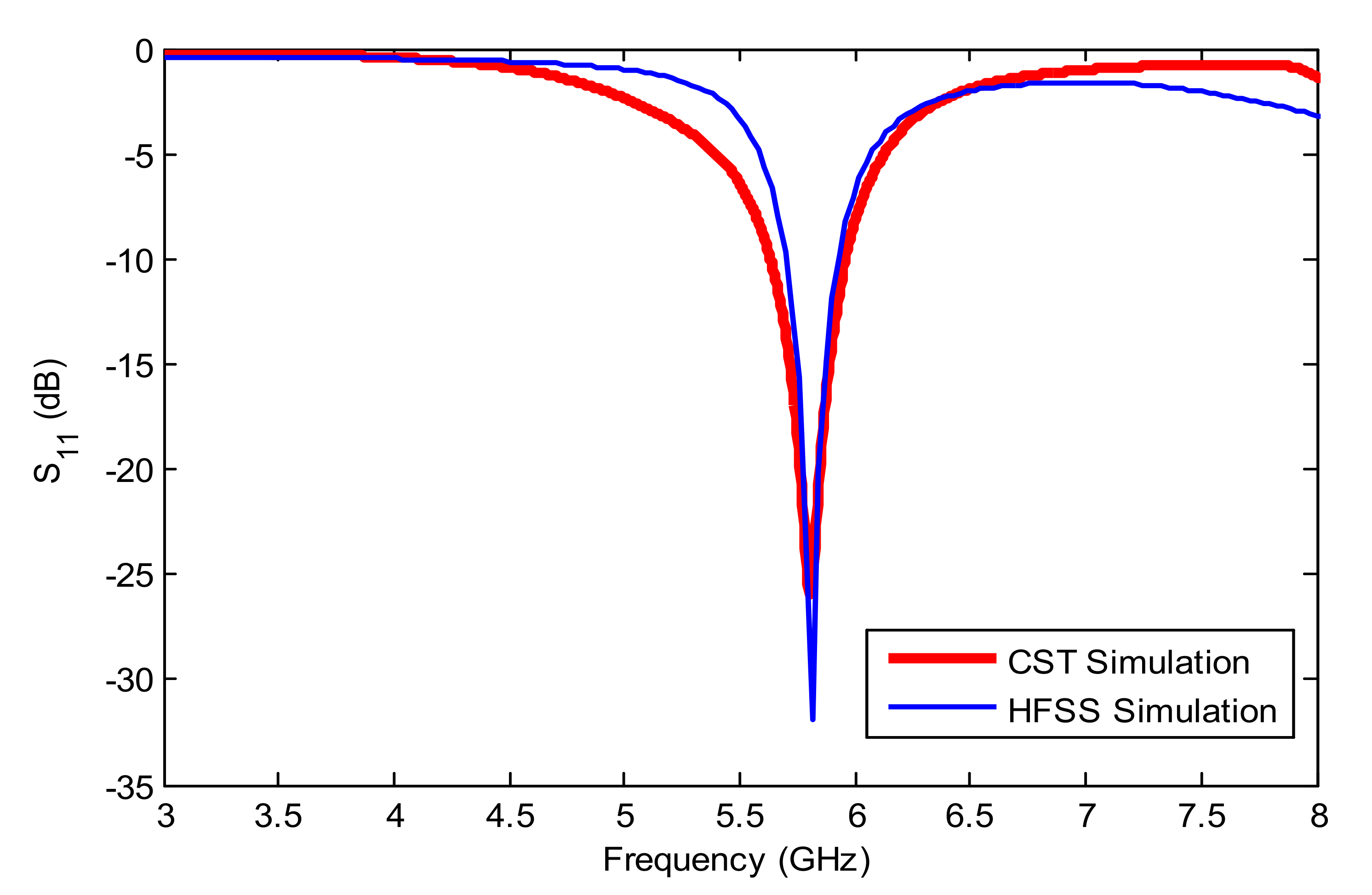
3.1. Miniaturization of the Microstrip Patch Antenna
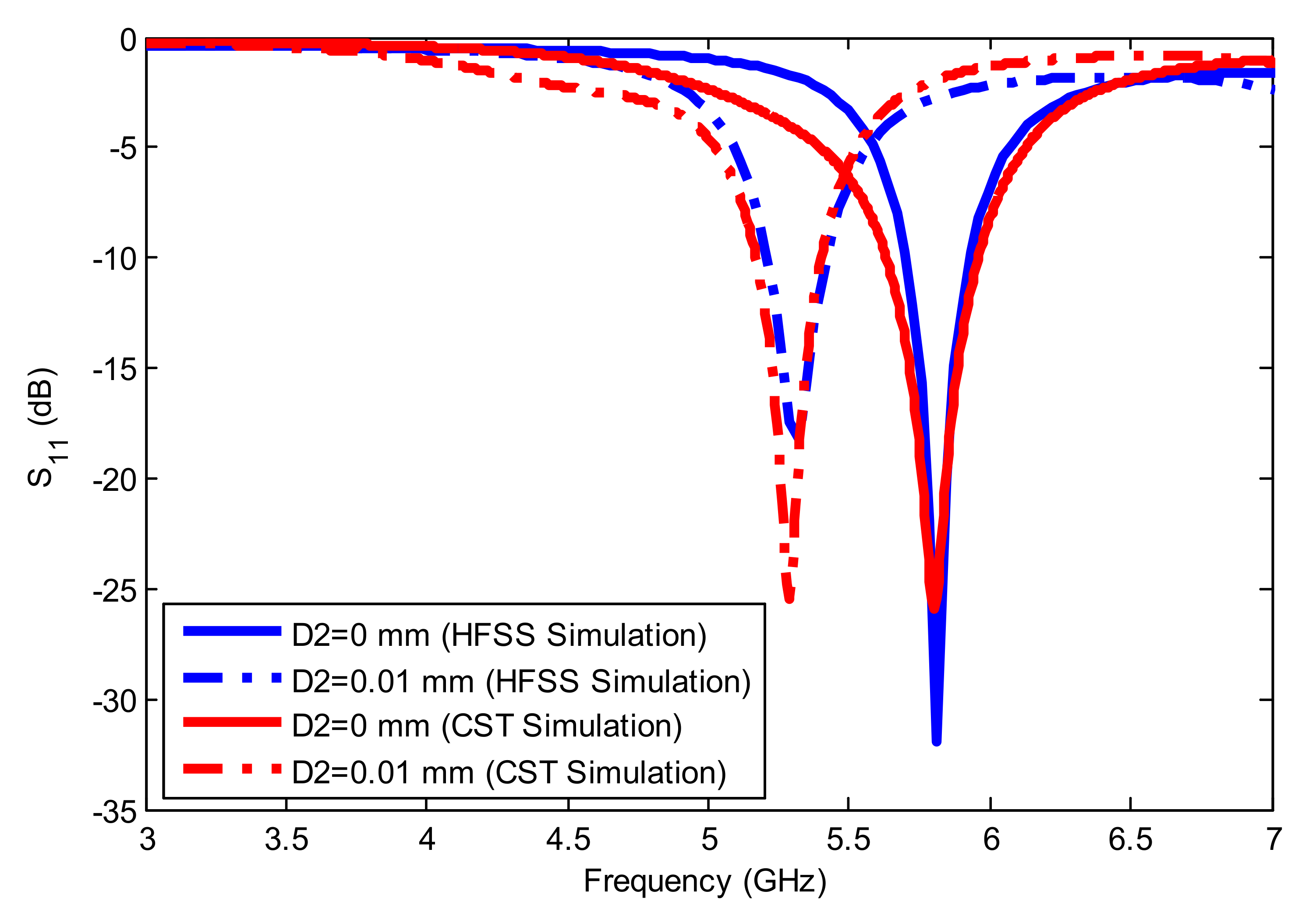
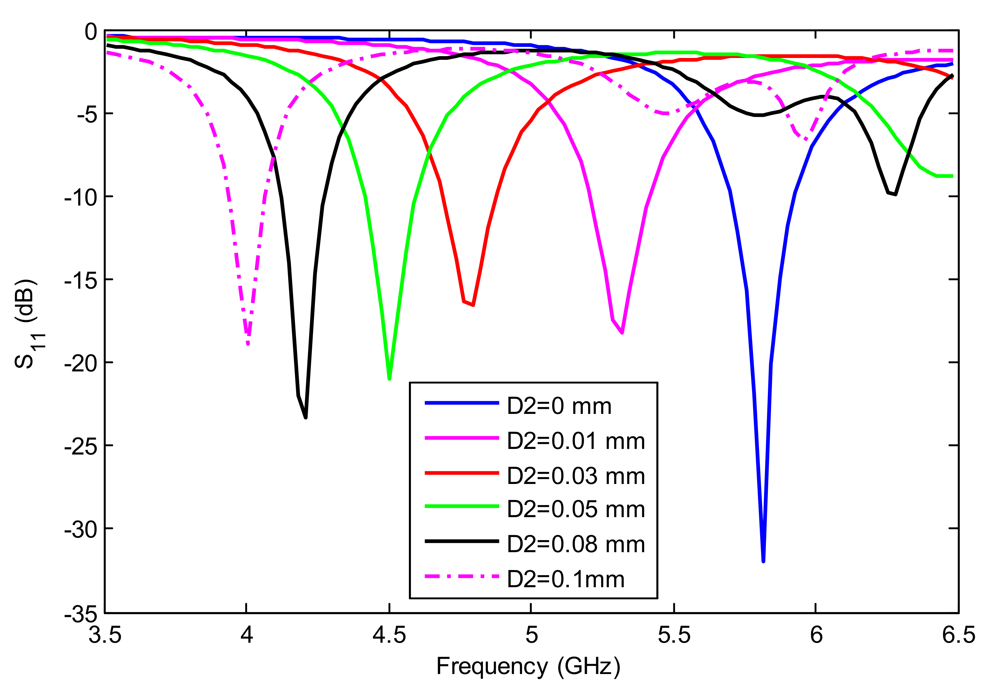
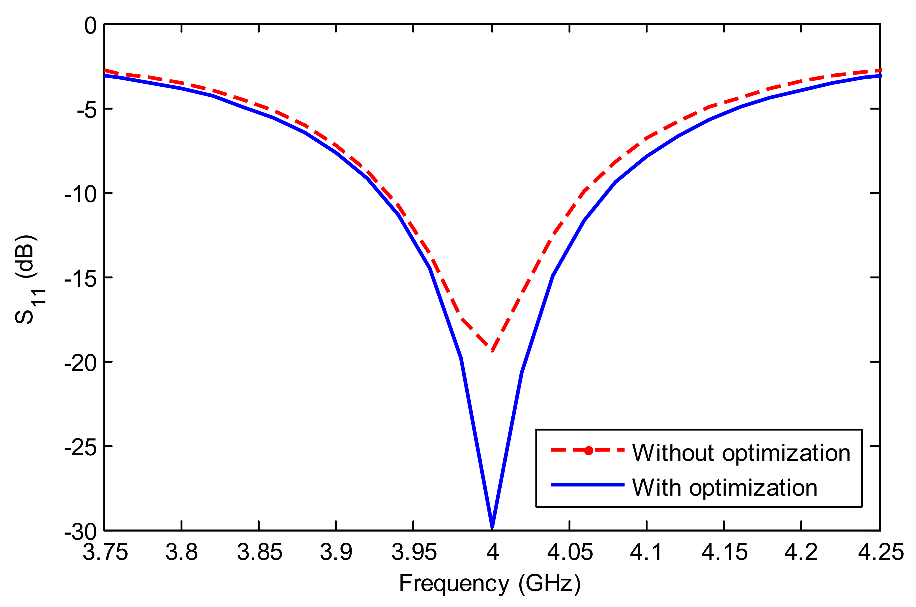
3.2. GA-Optimization of the Antenna with a Thin-Film Material with High Permittivity
4. Conclusions
Author Contributions
Funding
Institutional Review Board Statement
Informed Consent Statement
Data Availability Statement
Acknowledgments
Conflicts of Interest
References
- Bafleur, M.; Dilhac, J.-M. Towards Energy Autonomy of Wireless Sensors in Aeronautics Applications: SMARTER Collaborative Project. In Proceedings of the 2013 IEEE International Conference on Green Computing and Communications and IEEE Internet of Things and IEEE Cyber, Physical and Social Computing, Beijing, China, 20–23 August 2013. [Google Scholar]
- Affonso, E.T.; Nunes, R.D.; Rosa, R.L.; Pivaro, G.F.; Rodríguez, D.Z. Speech Quality Assessment in Wireless VoIP Communication Using Deep Belief Network. IEEE Access 2018, 6, 77022–77032. [Google Scholar] [CrossRef]
- Bertrand, A. Distributed Signal Processing for Wireless EEG Sensor Networks. IEEE Trans. Neural Syst. Rehabil. Eng. 2015, 23, 923–935. [Google Scholar] [CrossRef] [Green Version]
- Chakkor, S.; Baghouri, M.; Cheker, Z.; el Oualkadi, A.; el Hangouche, J.A.; Laamech, J. Intelligent Network for Proactive Detection of COVID-19 Disease. In Proceedings of the 2020 6th IEEE Congress on Information Science and Technology (CiSt), Agadir-Essaouira, Morocco, 5–12 June 2021. [Google Scholar]
- Lee, H.; Tak, J.; Choi, J. Wearable Antenna Integrated into Military Berets for Indoor/Outdoor Positioning System. IEEE Antennas Wirel. Propag. Lett. 2017, 16, 1919–1922. [Google Scholar] [CrossRef]
- Picon, O.; Cirio, L.; Ripoll, C.; Baudoin, G.; Bercher, J.-F.; Villegas, M. Les Antennes: Théorie, Conception et Applications; Dunod: Paris, France, 2009. [Google Scholar]
- Reddaf, A.; Djerfaf, F.; Ferroudji, K.; Boudjerda, M.; Hamdi-Chérif, K.; Bouchachi, I. Design of dual-band antenna using an optimized complementary split ring resonator. Appl. Phys. A 2019, 125, 186. [Google Scholar] [CrossRef]
- Chetouah, F.; Aidel, S.; Bouzit, N.; Messaoudene, I. A miniaturizedprinted monopole antenna for 5.2–5.8 GHz WLAN applications. Int. J. RF Microw. Comput.-Aided Eng. 2018, 28, e21250. [Google Scholar] [CrossRef]
- Fomundam, L.; Lin, J. Design of miniaturized high frequency printed coils for wireless power transfer to biomedical implants. In Proceedings of the 2016 16th Mediterranean Microwave Symposium (MMS), Abu Dhabi, United Arab Emirates, 14–16 November 2016. [Google Scholar]
- Wang, Z.; Zhang, H.; Yang, Y.; Qu, H.; Han, Z.; Pang, W.; Duan, X. Wireless Controlled Local Heating and Mixing Multiple Droplets Using Micro-Fabricated Resonator Array for Micro-Reactor Applications. IEEE Access 2017, 5, 25987–25992. [Google Scholar] [CrossRef]
- Rao, S.K. Advanced Antenna Technologies for Satellite Communications Payloads. IEEE Trans. Antennas Propag. 2015, 63, 1205–1217. [Google Scholar] [CrossRef]
- Deng, W.; Li, Z.; Xia, Y.; Wang, K.; Pei, W. A Widely Linear MMSE Anti-Collision Method for Multi-Antenna RFID Reader. IEEE Commun. Lett. 2019, 23, 644–647. [Google Scholar] [CrossRef]
- Ren, A.; Liu, Y.; Sim, C.-Y.-D. A Compact Building Block with Two Shared-Aperture Antennas for Eight-Antenna MIMO Array in Metal-Rimmed Smartphone. IEEE Trans. Antennas Propag. 2019, 67, 6430–6438. [Google Scholar] [CrossRef]
- Wong, K.; Tsai, C.; Lu, J. Two Asymmetrically Mirrored Gap-Coupled Loop Antennas as a Compact Building Block for Eight-Antenna MIMOArray in the Future Smartphone. IEEE Trans. Antennas Propag. 2017, 65, 1765–1778. [Google Scholar] [CrossRef]
- Blake, L.V.; Long, M.W. Antennas: Fundamentals, Design, Measurement, 3rd ed.; Scitech Publishing: New York, NY, USA, 2009. [Google Scholar]
- Guhaand, D.; Antar, Y.M.M. Microstrip and Printed Antennas: New Trends Techniques and Applications, 1st ed.; John Wiley & Sons: New York, NY, USA, 2011. [Google Scholar]
- Khan, M.U.; Sharawi, M.S.; Mittra, R. Microstrip patch antenna miniaturisation techniques: A review. IET Microw. Antennas Propag. 2015, 9, 913–922. [Google Scholar] [CrossRef]
- Wong, K.L. Planar Antennas for Wireless Communications, 1st ed.; John Wileyand Sons: Hoboken, NJ, USA, 2003. [Google Scholar]
- Herscovici, N.; Osorio, M.F. Miniaturization of rectangular microstrip patches using genetic algorithms. IEEE Antennas Wirel. Propag. Lett. 2002, 1, 94–97. [Google Scholar] [CrossRef]
- Waterhouse, R. Small microstrip patch antenna. Electron. Lett. 1995, 31, 604–605. [Google Scholar] [CrossRef]
- Gianvittorio, J.; Samii, Y. Fractal antennas: A novel antenna miniaturization technique, and applications. IEEE Antennas Propag. Mag. 2002, 44, 20–36. [Google Scholar] [CrossRef]
- Sharawi, M.S.; Khan, M.U.; Numan, A.B.; Aloi, D.N. A CSRR Loaded MIMO Antenna System for ISM Band Operation. IEEE Trans. Antennas Propag. 2013, AP-61, 4265–4274. [Google Scholar] [CrossRef]
- Liu, J.X.; Yin, W.Y.; He, S.L. A new defected ground structure and its application for miniaturized switchable antenna. Prog. Electromagn. Res. 2010, 107, 115–128. [Google Scholar] [CrossRef] [Green Version]
- Altunyurt, N.; Swaminathan, M.; Raj, P.M.; Nair, V. Antenna miniaturization using magneto-dielectric substrates. In Proceedings of the 2009 59th Electronic Components and Technology Conference, San Diego, CA, USA, 26–29 May 2009. [Google Scholar]
- Constantine, A.B. Antenna Theory: Analysis and Design, 3rd ed.; John Wileyand Sons: Hoboken, NJ, USA, 2005. [Google Scholar]
- Boudjerda, M.; Reddaf, A.; Ferrouji, K.; Messaoudene, I.; Bouchachi, I. Numerical Investigations of a Reconfigurable Patch Antenna using Thin Ferrite Film. In Proceedings of the 5th International Conference on Welding, Non Destructive Testingand Materials and Alloys Industry (IC-WNDT-MI’16), Oran, Algeria, 26–28 November 2016. [Google Scholar]
- Volakis, J.L.; Chen, C.-C.; Fujimoto, K.Y. Small Antennas: Miniaturization Techniques and Applications, 1st ed.; McGraw Hill: New York, NY, USA, 2008. [Google Scholar]
- Bhartia, P.; Bahl, I.; Garg, R.; Ittipiboon, A. Microstrip Antenna Design Handbook, 1st ed.; Artech House Publishers: Boston, MA, USA, 2000. [Google Scholar]
- Reddaf, A.; Djerfaf, F.; Ferroudji, K.; Boudjerda, M.; Hamdi-Chérif, K.; Bouchachi, I. Modeling of electromagnetic behavior of composite thin layers using genetic algorithm. Math. Comput. Simul. 2020, 167, 281–295. [Google Scholar] [CrossRef]
- Johnson, J.M.; Rahmat-Samii, Y. Genetic algorithms in engineering elecromagnetics. IEEE Trans. Antennas Propag. 1997, 39, 7–21. [Google Scholar] [CrossRef] [Green Version]
- Weile, D.S.; Michielssen, E. Genetic algorithm optimization applied to electromagnetics: A review. IEEE Trans. Antennas Propag. 1997, 45, 343–353. [Google Scholar] [CrossRef]
- Jayasinghe, J.M.J.W.; Uduwawala, D.N. A broadband triple-frequency patch antenna for WLAN applications using genetic algorithm optimization. In Proceedings of the 2012 IEEE 7th International Conference on Industrial and Information Systems (ICIIS), Chennai, India, 6–9 August 2012. [Google Scholar]
- RenugaKanni, V.; Brinda, R. Design of High Gain Microstrip Antenna for Vehicle to Vehicle Communication Using Genetic Algorithm. Prog. Electromagn. Res. M 2019, 81, 167–179. [Google Scholar] [CrossRef] [Green Version]
- Lamsalli, M.; Hamichi, A.E.; Boussouis, M.; Touhami, N.A.; Elhamadi, T. Genetic Algorithm Optimization ForMicrostrip Patch Antenna Miniaturization. Prog. Electromagn. Res. Lett. 2016, 60, 113–120. [Google Scholar] [CrossRef] [Green Version]
- Elftouh, H.; Touhami, N.A.; Aghoutane, M. Miniaturized Microstrip Patch Antenna with Spiral Defected Microstrip Structure. Prog. Electromagn. Res. Lett. 2015, 53, 37–44. [Google Scholar] [CrossRef] [Green Version]
- Dhakshinamoorthi, M.K.; Gokulakkrizhna, S.; Subha, M.; Mekaladevi, V. Rectangular Microstrip Patch Antenna Miniaturization using improvised Genetic Algorithm. In Proceedings of the 2020 4th International Conference on Trends in Electronics and Informatics (ICOEI 2020), Tirunelveli, India, 15–17 June 2020. [Google Scholar]
- Yang, S.; Zhang, L.; Fu, J.; Zheng, Z.; Zhang, X.; Liao, M. Design and optimization for 77 GHz series-fed patch array antenna based on genetic algorithm. Sensors 2020, 20, 3066. [Google Scholar] [CrossRef] [PubMed]
- Gjokaj, V.; Doroshewitz, J.; Nanzer, J.; Chahal, P. A Design Study of 5G Antennas Optimized Using Genetic Algorithms. In Proceedings of the 2017 IEEE 67th Electronic Components and Technology Conference (ECTC), Orlando, FL, USA, 30 May–2 June 2017. [Google Scholar]
- Wang, S.C.; Mao, Y.J.; Li, M.J.; Yang, H.K.; Tong, M.S. A Novel Design of Multiband Antenna Based on Non-dominated Sorting Genetic Algorithm. In Proceedings of the 2019 IEEE International Symposium on Antennas and Propagation and USNC-URSI Radio Science Meeting 2019, Atlanta, GA, USA, 7–12 July 2019. [Google Scholar]
- Wee, F.H.; Malek, F. Gain Enhancement of a Microstrip Patch Antenna using Array Rectangular Barium Strontium Titanate (BST). In Proceedings of the 2011 Loughborough Antennas and Propagation Conference, Loughborough, UK, 14–15 November 2011. [Google Scholar]
- Messaoudene, I.; Chetouah, F.; Belazoug, M. Compact Rectangular DRA with High Permittivity Stacked Resonator for RADAR Applications. In Proceedings of the 7th Seminar on Detection Systems: Architectures and Technologies (DAT’2017), Algiers, Algeria, 20–22 February 2017. [Google Scholar]
- Huang, Y.; Boyle, K. Antennas: From Theory to Practice, 1st ed.; John Wiley & Sons Ltd.: Singapore, 2008. [Google Scholar]
- Jackson, D.R.; Alexopoulos, N.G. Simple Approximate Formulas for Input Resistance Bandwidth and Efficiency of a Resonant Rectangular Patch. IEEE Trans. Antennas Propag. 1991, 39, 407–410. [Google Scholar] [CrossRef]
- Lowen, R.; Verschoren, A. Foundations of Generic Optimization: Volume 2: Applications of Fuzzy Control, Genetic Algorithms and Neural Networks, 1st ed.; Springer: Berlin, Germany, 2008. [Google Scholar]
- Bouchachi, I.; Hamdi-Cherif, K.; Ferroudji, K.; Boudjreda, M.; Reddaf, A.; Riabi, M.L.A. Comparison of Genetic Algorithm and Practical Swarm Optimization for the Design of Waveguide Filters. In Lecture Notes in Electrical Engineering; Springer: Singapore, 2019; pp. 89–98. [Google Scholar]
- Haupt, R.L.; Haupt, S.E. Practical Genetic Algorithms, 2nd ed.; John Wiley & Sons Inc.: Hoboken, NJ, USA, 2004. [Google Scholar]
- Mishra, S.; Sahoo, S.; Das, M. Genetic Algorithm: An Efficient Tool for Global Optimization. Adv. Comput. Sci. Technol. 2017, 10, 2201–2211. [Google Scholar]
- Chiroma, H.; Abdulkareem, S.; Abubakar, A.; Zeki, A.; Gital, A.Y.U.; Usman, M.J. Correlation study of genetic algorithm perators: Crossover and mutation probabilities. In Proceedings of the International Symposium on Mathematical Sciences and Computing Research 2013, Perak, Malaysia, 6–7 December 2013. [Google Scholar]
- Patil, V.P.; Pawar, D.D. The optimal crossover or mutation rates in genetic algorithm: A review. Int. J. Appl. Eng. Technol. 2015, 5, 38–41. [Google Scholar]
- Johnson, J.M.; Rahmat-Samii, Y. Genetic algorithms and method of moments (GA/Mom) for the design of integrated antennas. IEEE Trans. Antennas Propag. 1999, 47, 1606–1614. [Google Scholar] [CrossRef]
- Soontornpipit, P.C.; Furse, M.; Chung, Y.C. Miniaturized biocompatible microstrip antenna using genetic algorithm. IEEE Trans. Antennas Propag. 2005, 53, 1939–1945. [Google Scholar] [CrossRef]

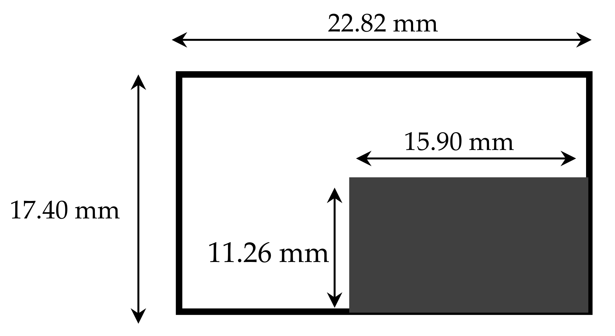
| W1 × L1 (mm2) | W2 × L2 (mm2) | W3 × L3 (mm2) | D1 (mm) | W2 (mm) |
|---|---|---|---|---|
| 15.9 × 11.26 | 0.71 × 13.31 | 3.02 × 11.81 | 1.58 | 0.01–0.1 |
| Antenna | Patch Dimensions (W1 × L1) (mm2) | Return Loss (dB) | Bandwith (MHz) | VSWR | Gain (dB) |
|---|---|---|---|---|---|
| Conventional | 22.1 × 16.84 (372.16) | −33.7 | 118.4 | 1.04 | 3.88 |
| With thin film | 15.90 × 11.26 (179.04) | −19.42 | 127.4 | 1.86 | 3.89 |
| With thin film and GA | 13.76 × 11.32 (155.04) | −29.81 | 147.8 | 1.06 | 3.63 |
| Antenna | (GHz) | (GHz) | Return Loss (dB) | Bandwith (MHz) | Miniaturization Rate (%) | Gain (dB) |
|---|---|---|---|---|---|---|
| N. Herscovici et al. [19] | 3.000 | 1.738 | −24 | 10 | 42 | 1 |
| P. Soontornpipit et al. [51] | 0.405 | 0.4035 | −15 | 20 | / | / |
| H. Elftouh et al. [35] | 5.700 | 3.000 | ≈−38 | / | 50 | 2.14 |
| M. Lamsalli et al. [34] | 4.900 | 2.160 | −20 | ≈10 | 82 | 5.82 |
| M. S. Sharawi et al. [22] | 5.040 | 2.450 | ≈−25 | ≈50 | 76 | −0.8 |
| M K. Dhakshinamoorthi et al. [36] | 3.000 | 2.3958 | −12.5 | 30 | 24.4 | / |
| 4.000 | 2.4022 | −13.5 | 22 | 45.8 | / | |
| Proposed | 5.800 | 4.000 | −29.81 | 147.8 | ≈60 | 3.63 |
Publisher’s Note: MDPI stays neutral with regard to jurisdictional claims in published maps and institutional affiliations. |
© 2022 by the authors. Licensee MDPI, Basel, Switzerland. This article is an open access article distributed under the terms and conditions of the Creative Commons Attribution (CC BY) license (https://creativecommons.org/licenses/by/4.0/).
Share and Cite
Boudjerda, M.; Reddaf, A.; Kacha, A.; Hamdi-Cherif, K.; Alharbi, T.E.A.; Alzaidi, M.S.; Alsharef, M.; Ghoneim, S.S.M. Design and Optimization of Miniaturized Microstrip Patch Antennas Using a Genetic Algorithm. Electronics 2022, 11, 2123. https://doi.org/10.3390/electronics11142123
Boudjerda M, Reddaf A, Kacha A, Hamdi-Cherif K, Alharbi TEA, Alzaidi MS, Alsharef M, Ghoneim SSM. Design and Optimization of Miniaturized Microstrip Patch Antennas Using a Genetic Algorithm. Electronics. 2022; 11(14):2123. https://doi.org/10.3390/electronics11142123
Chicago/Turabian StyleBoudjerda, Mounir, Abdelmalek Reddaf, Abdellah Kacha, Khaled Hamdi-Cherif, Turki E. A. Alharbi, Mohammed S. Alzaidi, Mohammad Alsharef, and Sherif S. M. Ghoneim. 2022. "Design and Optimization of Miniaturized Microstrip Patch Antennas Using a Genetic Algorithm" Electronics 11, no. 14: 2123. https://doi.org/10.3390/electronics11142123