Article

X-Band In-Line Coaxial-to-Groove Gap Waveguide Transition

by
Riccardo Rossi
and
Roberto Vincenti Gatti
*
Department of Engineering, University of Perugia, Via G. Duranti 93, 06125 Perugia, Italy
*
Author to whom correspondence should be addressed.
Electronics 2022, 11(15), 2361; https://doi.org/10.3390/electronics11152361
Submission received: 9 June 2022 / Revised: 27 June 2022 / Accepted: 25 July 2022 / Published: 28 July 2022
(This article belongs to the Section Microwave and Wireless Communications)

Abstract

:
A coaxial-to-groove gap waveguide transition is proposed for the first time, addressing the lack of similar designs in the state-of-the-art literature. An in-line configuration is adopted in case of stringent space requirements in groove gap waveguide systems. This device has no dielectric and makes use of a waveguide multi-step ridged section connected to the inner conductor of a coaxial line. Three versions are presented, covering progressively wider bandwidths depending on the number of employed steps. The three configurations achieve 20-dB return loss fractional bandwidths of 2.63%, 16.79%, and 38.08%, and 30-dB return loss fractional bandwidths of 0.84%, 10.63%, and 33.49%, with a simulated insertion loss always better than 0.05 dB when a realistic metal conductivity of 2 × 10 7 S/m is assumed. A tolerance analysis on the most critical geometrical parameters is provided to assess the mechanical feasibility, preserving a remarkable performance at X band.

1. Introduction

Most modern microwave devices and systems based on standard rectangular waveguides (RWs) are fabricated in split blocks and connected by means of screwing, diffusion bonding, or deep-brazing techniques [1,2]. Very good electrical contact between the manufactured parts as well as good alignment are needed, as severe electrical performance degradation may be produced by small gaps on the contact surface. This aspect becomes more and more critical as the operating frequency is increased, since high-precision manufacturing and assembling are required, leading to a higher cost. Gap waveguides have been recently introduced to cope with this problem.
The ideal gap waveguide consists of stacking a perfect magnetic conductor (PMC) and a perfect electric conductor (PEC) separated by an air gap in a parallel-plate waveguide configuration [3,4]. Wave propagation is forbidden between the plates as long as the gap separation is less than a quarter wavelength. Since a PMC does not exist in nature, its condition is emulated by an artificial magnetic conductor (AMC) in the form of periodic textured structures, among which the most known is the bed of nails realized by periodic metal pins. This high-impedance surface creates a stopband over which parallel-plate modes cannot propagate. The groove gap waveguide (GGW) consists of incorporating a guiding section in the form of a groove in the bed of nails. In this way, as a consequence of the stopband, the electromagnetic wave is confined in the groove without leaking in lateral directions. The GGW is very similar to the RW, though its main advantage is that an electrical contact between the upper and lower metal surfaces is no longer needed, thus relaxing mechanical requirements. As a consequence, GGW insertion loss only depends on the effective metal conductivity and excellent electrical performance is achieved even at very high frequencies. In addition to this, the absence of a dielectric makes this technology appealing for the design of low-loss components.
Transitions between transmission lines play an essential role in any microwave system since a good matching between its various components is required in order to obtain maximum power transfer. Moreover, they are important in any measurement problem, as they contribute to the assessment of the device under test (DUT) performance [5,6,7,8]. For this reason, the design of an interface from a GGW to a piece of measurement equipment or to any other device is of great interest. Transitions from GGW to RW are investigated in [9,10,11,12]. These designs employ hollow metallic RWs, thus allowing high power levels without dielectric losses. Nevertheless, RWs are perpendicularly connected to GGWs and the right-angle configuration can represent a limitation in space-constrained systems. More generally, the need for an in-line transition may be imposed by the system requirements. GGW end launchers are discussed in [13,14,15,16]. These in-line configurations make use of microstrip matching sections; however, the inherent presence of a substrate material leads to undesired losses in high-performance systems.
In this paper, a coaxial-to-GGW in-line transition at X band is proposed. To the authors’ best knowledge, this is the first time that a device of this kind is presented. This component meets the requirement of continuity along the longitudinal axis between the two transmission lines without introducing a dielectric substrate and can be employed to feed or measure GGW devices. This transition makes use of a multi-step ridged section connected to the coaxial line inner conductor. Three designs are outlined adopting a ridge with two, three, and five steps, covering progressively wider bandwidths. A tolerance analysis of the most critical parameters is provided to assess the device’s feasibility. All simulations are performed using the commercial 3D full-wave software CST Microwave Studio.

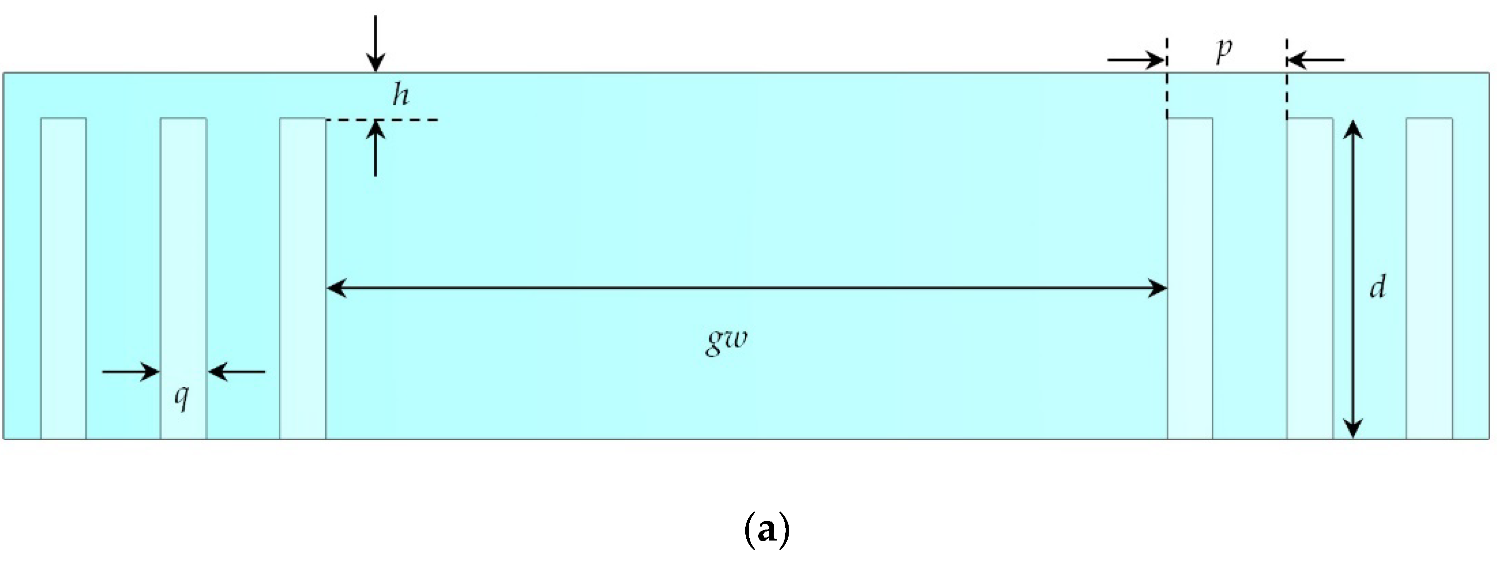
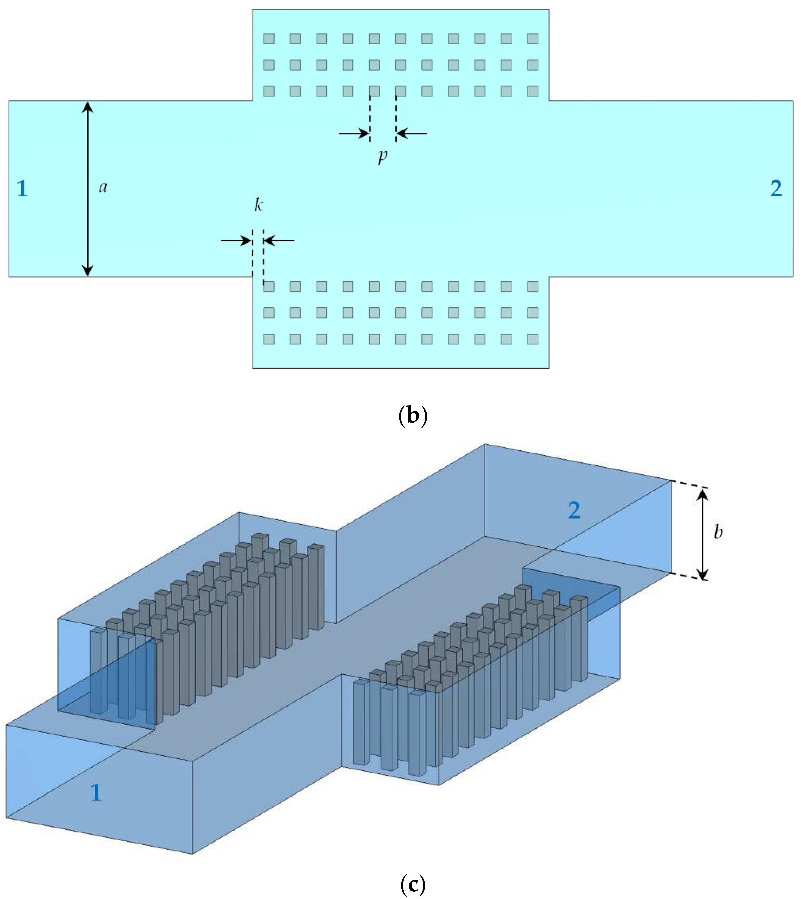
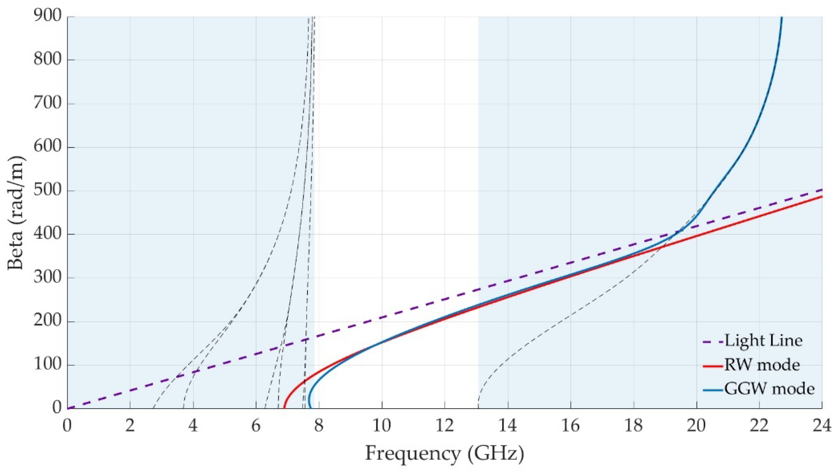
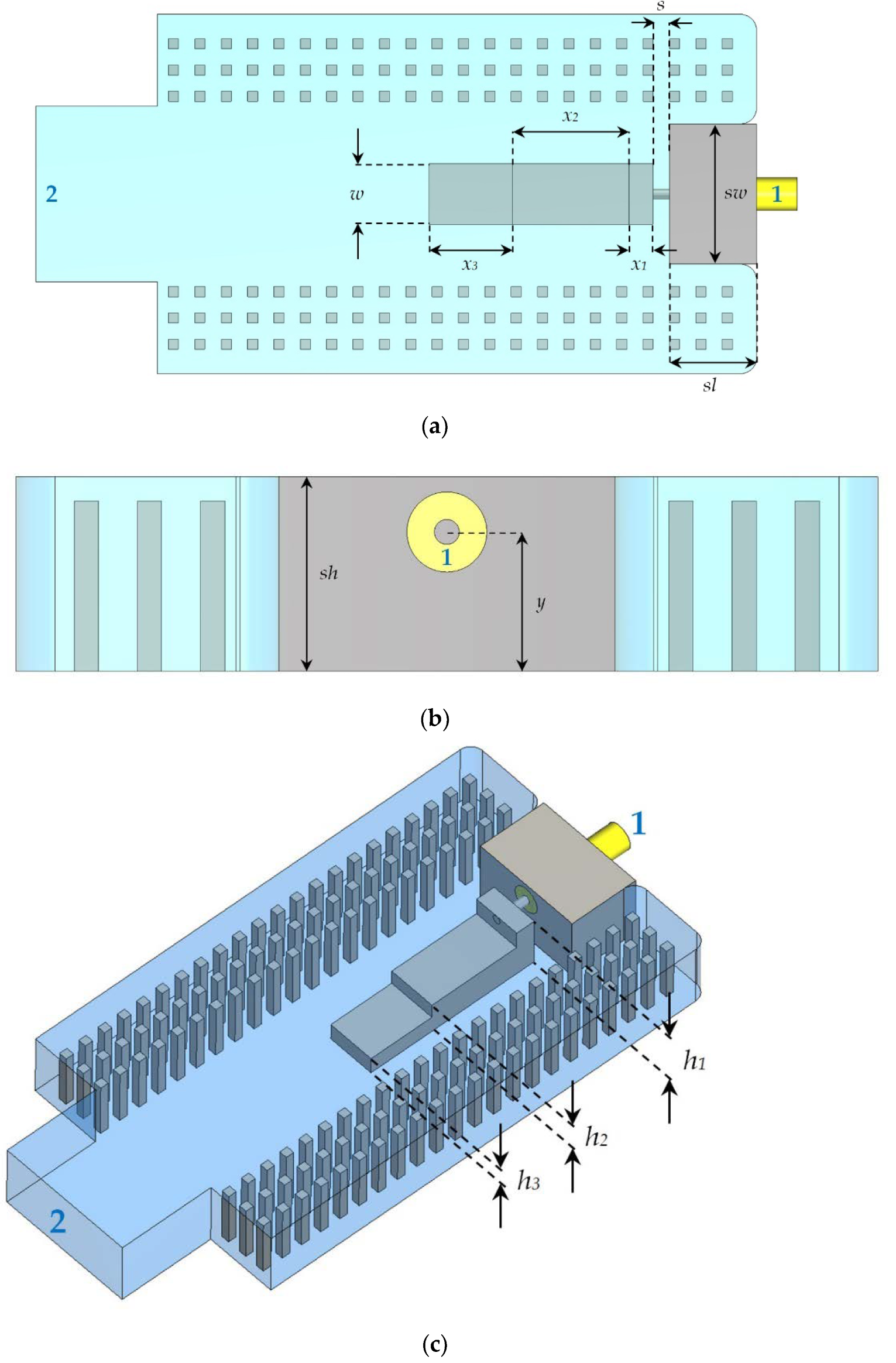
2. Groove Gap Waveguide Design

The gap waveguide stopband is defined as the frequency range for which the propagation of parallel-plate modes is inhibited. Such a range depends on the gap waveguide geometrical parameters, in particular the air gap height h, the pin height d, the pitch between two adjacent pins p, and the pin side q. A suitable GGW geometry for X-band operation is selected following the guidelines in [17] and is shown in Figure 1. Pins are arranged according to a square lattice and the bed of nails is truncated on each side after the third row of pins with no performance degradation [18]. The material used in the following simulations is PEC with zero surface roughness. PEC boundary conditions surround the top, bottom, and lateral faces.
As for a standard RW, a dispersive mode very similar to the TE10 mode propagates through the groove inside the stopband. The GGW dispersion diagrams are calculated using the eigenmode solver in CST Microwave Studio and presented in Figure 2. From an analysis of the first eight propagating modes, the resulting stopband ranges from 7.86 GHz to 13.07 GHz, thus covering the whole X band. It is well known that electromagnetic simulation software requires continuous cross-section waveguide ports. Given the resemblance between the RW and the GGW, usually the numerical ports are directly attached to the GGW [19], but this does not guarantee a perfect impedance matching. For this reason, an equivalent RW is defined, with width a and height b = d + h, separated from the first row of pins by a distance k. The parameters a and k for the geometry in Figure 1b are selected for optimum return loss, as reported in Figure 3. The propagation constant of the equivalent RW is also indicated in Figure 2, showing that the fundamental modes of the two waveguides are very similar within the stopband. The GGW geometrical parameters are listed in Table 1.

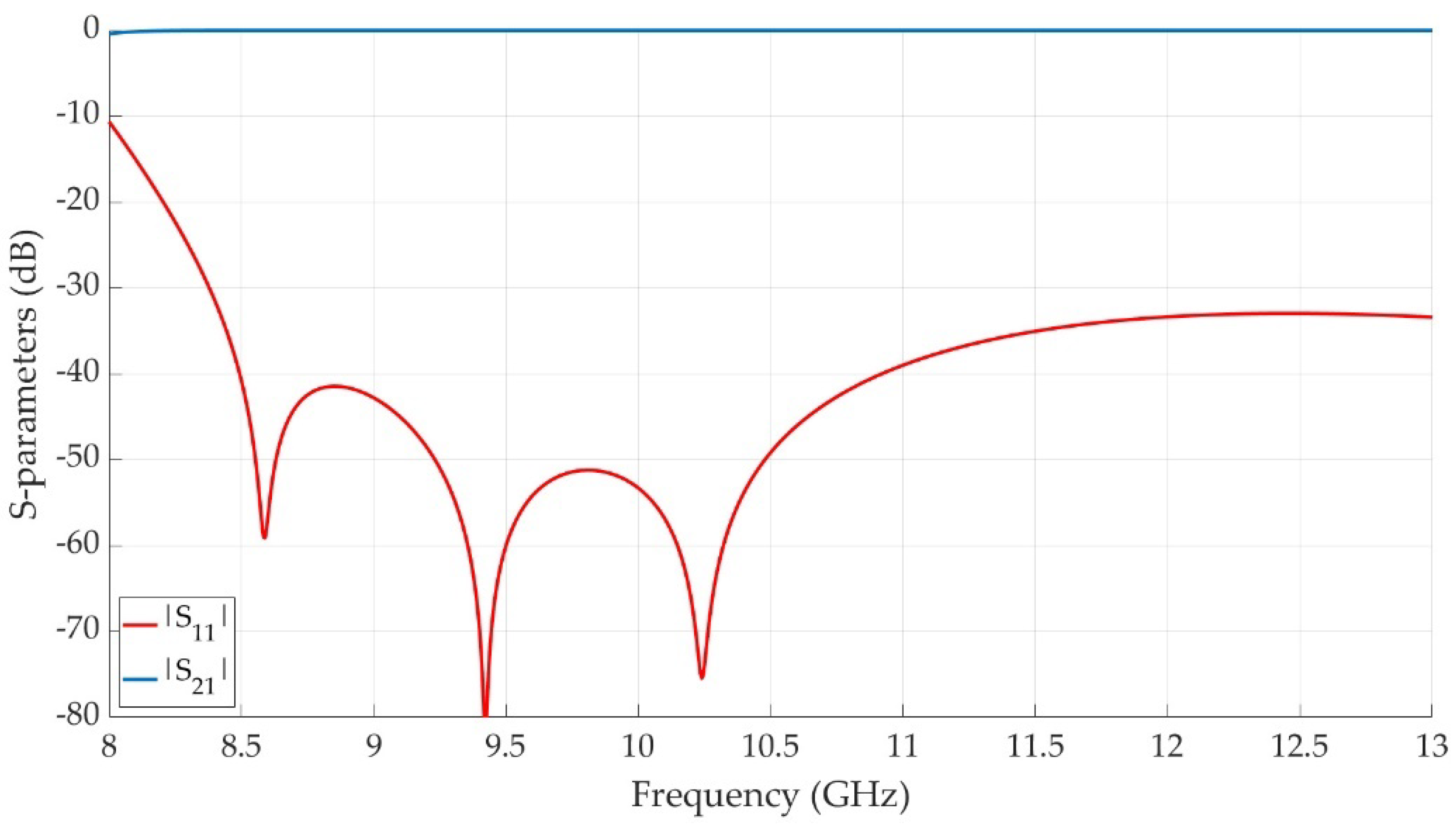
3. Transition Design

Three coaxial-to-GGW in-line transitions with increasing bandwidths are designed. An SMA coaxial connector enters the GGW through a waveguide short in the form of a solid metal block, and the inner conductor is in electrical contact with a multi-section metallic ridge. The three versions differ according to the number of steps used in the ridge section. In particular, the narrowband (NB) device has two steps, the intermediate bandwidth (IB) component has three steps, and the wideband (WB) version has five steps. The coaxial-to-GGW transition geometry is shown in Figure 4, where only the IB design is reported for brevity. The material used is aluminum with an estimated surface of 0.5 µm, leading to an effective conductivity equal to σ = 2 × 10⁷ S/m. The metallic background is hidden for better understanding. As represented in Figure 4b, the metal block shorts the GGW top and bottom walls. This block cannot have a different height, as a parallel-plate mode propagation would be triggered, thus degrading the overall performance. Nevertheless, since a prototype realization would assume two split blocks, from a manufacturing point of view it is easier to ensure a good electrica l contact on a small localized surface rather than around the entire perimeter of the groove with screws or other techniques. A blending radius of 2 mm is used to round off internal edges in the case of CNC milling machine manufacturing. The full set of geometrical parameters for the three devices and the corresponding simulated scattering parameters are shown in Table 2 and Figure 5, respectively. The bandwidths with return loss better than 30 dB range from 9.37 GHz to 9.62 GHz for the NB version, from 8.73 GHz to 10.33 GHz for the IB version, and from 8.42 GHz to 12.38 GHz for the WB version. The corresponding fractional bandwidths are 2.63%, 16.79%, and 38.08%, respectively. The bandwidths with return loss better than 30 dB range from 9.46 GHz to 9.54 GHz for the NB version, from 9.00 GHz to 10.01 GHz for the IB version, and from 8.60 GHz to 12.06 GHz for the WB version. The corresponding fractional bandwidths are 0.84%, 10.63%, and 33.49%, respectively. Negligible insertion loss is observed in these frequency intervals.

4. Tolerance Analysis

Being closed structures in air-filled metallic waveguides, these transitions are suitable for prototyping using a CNC milling machine manufacturing process. The design robustness and reliability are evaluated for the IB version through a tolerance analysis simulation on the most critical geometrical parameters, in particular the step lengths x1, x2, and x3, the step heights h1, h2, and h3, the step width w, the distance between the short and the step s, the coaxial height y, and the pin height d. Numerical values are swept in a range of ±0.05 mm from the nominal for a total of 1024 simulations. This tolerance range is guaranteed by most modern CNC standards. Simulated results are illustrated in Figure 6 and compared to the nominal device, showing that a very good performance is preserved at X band.

5. Conclusions

GGW technology was recently introduced to provide a solution to the losses at microwave frequencies caused by an imperfect electrical contact between split blocks in the assembly of waveguide components. Transitions between different types of transmission lines are very important to feed or measure a variety of microwave devices and systems. In this paper, a coaxial-to-GGW transition has been presented for the first time. This component has no dielectric and presents an in-line configuration to be employed in space-constrained GGW systems. In this device, the GGW is end-fed by a coaxial line whose inner conductor is connected to a stepped ridge matching section. Three transitions have been designed adopting an increasing number of steps, reaching a 30-dB return loss bandwidth up to 33.49%. Mechanical robustness and reliability have been evaluated with a tolerance analysis of the most critical geometrical parameters, showing very good performance at X band.

Author Contributions

Conceptualization, R.R. and R.V.G.; data curation, R.R.; formal analysis, R.R. and R.V.G.; investigation, R.R.; methodology, R.R. and R.V.G.; project administration, R.V.G.; resources, R.V.G.; supervision, R.V.G.; validation, R.R.; visualization, R.R. and R.V.G.; writing—original draft, R.R.; writing—review & editing, R.R. and R.V.G. All authors have read and agreed to the published version of the manuscript.

Funding

This research received no external funding.

Institutional Review Board Statement

Not applicable.

Informed Consent Statement

Not applicable.

Data Availability Statement

Data is contained within the article.

Conflicts of Interest

The authors declare no conflict of interest.

References

  1. Vincenti Gatti, R.; Rossi, R.; Dionigi, M.; Spigarelli, A. An x-band compact and low-profile waveguide magic-t. Int. J. RF Microw. Comput. Eng. 2019, 29, e21854. [Google Scholar] [CrossRef]
  2. Vincenti Gatti, R.; Rossi, R.; Dionigi, M. Wideband rectangular waveguide to substrate integrated waveguide (siw) e-plane t-junction. Electronics 2021, 10, 264. [Google Scholar] [CrossRef]
  3. Chen, Z.N.; Liu, D.; Nakano, H.; Qing, X.; Zwick, T. Handbook of Antenna Technologies; Springer: Singapore, 2016. [Google Scholar]
  4. Rajo-Iglesias, E.; Ferrando-Rocher, M.; Zaman, A.U. Gap waveguide technology for millimeter-wave antenna systems. IEEE Commun. Mag. 2018, 56, 14–20. [Google Scholar] [CrossRef] [Green Version]
  5. Vincenti Gatti, R.; Rossi, R. Wideband compact single-ridge waveguide to rectangular waveguide transitions with integrated E -plane bend. Electron. Lett. 2016, 52, 1699–1701. [Google Scholar] [CrossRef]
  6. Vincenti Gatti, R.; Rossi, R.; Dionigi, M. X-band right-angle coaxial-to-single ridge waveguide compact transition with capacitive coupling. Electron. Lett. 2019, 55, 103–105. [Google Scholar] [CrossRef]
  7. Vincenti Gatti, R.; Rossi, R.; Dionigi, M. In-line stepped ridge coaxial-to-rectangular waveguide transition with capacitive coupling. Int. J. RF Microw. Comput. Eng. 2018, 29, e21626. [Google Scholar] [CrossRef]
  8. Vincenti Gatti, R.; Rossi, R.; Dionigi, M. Broadband right-angle rectangular waveguide to substrate integrated waveguide transition with distributed impedance matching network. Appl. Sci. 2019, 9, 389. [Google Scholar] [CrossRef] [Green Version]
  9. Farahbakhsh, A.; Zarifi, D.; Zaman, A.U. 60-GHz groove gap waveguide based wideband h-plane power dividers and transitions: For use in high-gain slot array antenna. IEEE Trans. Microw. Theory Technol. 2017, 65, 4111–4121. [Google Scholar] [CrossRef] [Green Version]
  10. Ferrando-Rocher, M.; Sánchez-Escnderos, D.; Herranz-Herruzo, J.I.; Valero-Nogueira, A. Design of broadband gap waveguide transitions for millimeter-wave antenna arrays. In Proceedings of the 2018 15th European Radar Conference (EuRAD), Madrid, Spain, 26–28 September 2018; IEEE: Manhattan, NY, USA, 2018; pp. 501–504. [Google Scholar] [CrossRef]
  11. Cheng, X.; Liu, Z.; Yao, Y.; Yu, T.; Yu, J.; Chen, X. Novel band gap waveguide for low-loss and dual band applications. IEEE Trans. Microw. Theory Tech 2022, 70, 2610–2621. [Google Scholar] [CrossRef]
  12. Vosoogh, A.; Zaman, A.U.; Yang, J. Simple and broadband transition between rectangular waveguide and groove gap waveguide for mm-wave applications. In Proceedings of the 2018 IEEE International Symposium on Antennas and Propagation & USNC/URSI National Radio Science Meeting, Boston, MA, USA, 8–13 July 2018; IEEE: Manhattan, NY, USA, 2018; pp. 1101–1102. [Google Scholar] [CrossRef] [Green Version]
  13. Zarifi, D.; Ashrafian, A. A Broadband transition from microstrip to groove gap waveguide for ka-band applications. In Proceedings of the 2020 14th European Conference on Antennas and Propagation (EuCAP), Copenhagen, Denmark, 15–20 March 2020; IEEE: Manhattan, NY, USA, 2020. [Google Scholar] [CrossRef]
  14. Perez-Escudero, J.M.; Torres-Garcia, A.E.; Gonzalo, R.; Ederra, I. A Chebyshev transformer-based microstri-to-groove-gap-waveguide inline transition for mmic packaging. IEEE Trans. Compon. Packag. Manuf. Technol. 2019, 9, 1595–1602. [Google Scholar] [CrossRef] [Green Version]
  15. Shi, Y.; Zhang, J.; Zeng, S.; Zhou, M. Novel w-band millimeter-wave transition from microstrip line to groove gap waveguide for mmic integration and antenna application. IEEE Trans. Antennas Propag. 2018, 66, 3172–3176. [Google Scholar] [CrossRef]
  16. Nandi, U.; Zaman, A.U.; Vosoogh, A.; Yang, J. Novel millimeter wave transition from microstrip line to groove gap waveguide for mmic packaging and antenna integration. IEEE Microw. Wirel. Compon. Lett. 2017, 27, 691–693. [Google Scholar] [CrossRef] [Green Version]
  17. Rajo-Iglesias, E.; Kildal, P.-S. Numerical studies of bandwidth of parallel-plate cut-off realised by a bed of nails, corrugations and mushroom-type electromagnetic bandgap for use in gap waveguides. IET Microw. Antennas Propag. 2011, 5, 282–289. [Google Scholar] [CrossRef] [Green Version]
  18. Kildal, P.-S.; Zaman, A.; Rajo-Iglesias, E.; Alfonso, E.; Valero-Nogueira, A. Design and experimental verification of ridge gap waveguide in bed of nails for parallel-plate mode suppression. IET Microw. Antennas Propag. 2011, 5, 262–270. [Google Scholar] [CrossRef]
  19. Raza, H.; Yang, J.; Kildal, P.; Alfonso, E. Resemblance between gap waveguides and hollow waveguides. IET Microw. Antennas Propag. 2013, 7, 1221–1227. [Google Scholar] [CrossRef] [Green Version]
Figure 1. Groove gap waveguide geometry. (a) Cross section. (b) Top view. (c) 3D view.
Electronics 11 02361 g001aElectronics 11 02361 g001b
Figure 2. Groove gap waveguide dispersion diagrams.
Electronics 11 02361 g002
Figure 3. Groove gap waveguide scattering parameters.
Electronics 11 02361 g003
Figure 4. Coaxial-to-GGW IB transition geometry. (a) Top view. (b) Back view. (c) 3D view.
Electronics 11 02361 g004
Figure 5. Coaxial-to-GGW transitions scattering parameters. (a) NB. (b) IB. (c) WB.
Electronics 11 02361 g005
Figure 6. Coaxial-to-GGW IB transition tolerance analysis. (a) |S11|. (b) |S21|.
Electronics 11 02361 g006
Table 1. Groove gap waveguide geometrical parameters.
ParameterDescriptionValue (mm)
aEq. waveguide width21.70
bEq. waveguide height10.00
dPin height8.75
gwGroove width22.86
hAir gap separation1.25
kEq. waveguide distance1.37
pPin pitch3.25
qPin side1.25
Table 2. Coaxial-to-GGW transitions geometrical parameters.
ParameterDescriptionNB Value (mm)IB Value (mm)WB Value (mm)
h1Step 1 height7.917.848.22
h2Step 2 height3.2216.065.23
h3Step 3 height-2.733.13
h4Step 4 height--1.65
h5Step 5 height--0.52
sSteps distance2.282.022.26
shShort height10.0010.0010.00
slShort length10.7510.7510.75
swShort width14.8417.2913.82
wSteps width9.087.573.11
x1Step 1 length17.422.983.15
x2Step 2 length11.3714.348.56
x3Step 3 length-10.3011.46
x4Step 4 length--11.45
x5Step 5 length--13.36
yCoaxial height7.538.749.00
Publisher’s Note: MDPI stays neutral with regard to jurisdictional claims in published maps and institutional affiliations.

