Article

An Interleaved Two Switch Soft-Switching Forward PWM Power Converter with Current Doubler Rectifier

by
Khairy Sayed
1,* and
Ahmed G. Abo-Khalil
2,3
1
Faculty of Engineering, Sohag University, Sohag 82524, Egypt
2
College of Engineering, University of Sharjah, Sharjah 27272, United Arab Emirates
3
Department of Electrical Engineering, College of Engineering, Assiut University, Assiut 71515, Egypt
*
Author to whom correspondence should be addressed.
Electronics 2022, 11(16), 2551; https://doi.org/10.3390/electronics11162551
Submission received: 4 July 2022 / Revised: 8 August 2022 / Accepted: 9 August 2022 / Published: 15 August 2022

Abstract

:
Forward converters have been broadly used in the power supply industry due to their simplicity, worthy efficiency, and low cost. A novel prototype soft-switched zero-voltage and zero-current ZVZC PWM DC-DC power converter with low voltage/current stresses is introduced for telecommunication power feeding in this paper. A new two-switch interleaved forward converter circuit is introduced to minimalize current circulation with no supplementary auxiliary snubber circuits. This converter circuit includes some outstanding benefits such as reduced components, improved efficiency, high power density and economic circuit configurations for high power conditioning applications. The simple operation principle is demonstrated on the basis of steady-state analysis. Furthermore, the effective feasibility of the proposed circuit topology is evaluated and verified practically for a 500 W–100 kHz prototype breadboard. The operation principle and steady-state characteristics are demonstrated from a theoretical point of view. To verify the practical effectiveness of the proposed power converter, a 500 W–100 kHz prototype converter using ultrafast IGBTs is implemented for a distributed telecommunication energy plant. The studied soft-switching converter is evaluated in comparison with the previously-proposed PWM converters in terms of voltage, current stresses, and operating efficiency.

1. Introduction

There is an increasing need to achieve higher power densities and efficiencies for power converters. This has increased the use of soft-switched converters due to the benefits of primary switch zero-voltage switching (ZVS) turn-on and zero-current switching (ZCS) turn-off [1]. In particular, half-bridge or full-bridge-based LLC technology [2,3], which is more suitable for medium to high power applications, is broadly used in practical designs. Energy efficiency and power density are very important features of today’s consumer electronics and industrial applications. In addition, high efficiency over a wide range of output power and the ability to operate over a wide input voltage range are important future prospects for DC-DC converters. To achieve high efficiency, it is necessary to reduce switching loss, especially in high frequency power converters. In addition, for light loads where switching loss and gate drive loss dominate [4,5], reducing switching loss is effective in achieving high efficiency. On the other hand, for relatively low power applications such as for PV systems with low power or auxiliary power in electric vehicles, a forward converter is usually recommended due to the simplicity of the design [4]. According to this, some studies on forward type resonant converters were carried out [4,5,6,7,8].
Operation at hard switching of the flyback and forward converters imposes high voltage and current spikes on their switches, due to presence of transformer leakage inductance. Furthermore, switching losses result in low conversion efficiency. A passive clamp circuit can be added to dissipate the energy stored in the leakage inductance [9] and reduce the voltage stress on the switch. However, the power conversion efficiency of the circuit has not improved significantly. In recent years, active clamping techniques have been proposed for both converters to absorb the energy stored in the leakage inductance and suppress transients across the switch. In addition, the forward converter energy reset process has been completed [10,11,12,13,14]. The active-clamping converters have higher efficiency than conventional forward and flyback converters because of the zero-voltage-switching (ZVS) operation of the main switch fulfilled with the help of the auxiliary switch.
Numerous types of soft-switching DC-DC power converters have been proposed. One of the most popular isolated power converters is the forward converter that has been widely implemented in low to medium power supply demands due to its simplicity, high reliability, and high efficiency [12]. The HF transformer in forward and flyback converter is used for isolating the electric power signal and storing the magnetic energy. The HF transformer in the forward converter is implemented to achieve galvanic isolation and energy transformation. Resetting the HF transformer is a special feature for the forward DC-DC converter. Therefore, several forward topologies have been suggested with diverse transformer reset arrangements [13,14,15,16,17].
Among these transformer resetting topologies, the two-switch forward DC-DC converter can realize the lowest voltage stresses on the primary-side active switches [17,18,19,20,21,22,23,24,25]. Moreover, the magnetizing and leakage energy can be recovered for attaining higher efficiency. Generally, the forward DC-DC converter is a promising choice in applications with high-output current requirements. The primary-side of these converters produces symmetrical AC waveforms across the primary-winding of the HF transformer. Therefore, the core flux is bi-directionally excited, resulting in a better utilization of magnetic core and results in increased power rating. Forward converters offer the advantage of better transformer utilization. Energy is transferred instantly through the transformer and not depending on energy storage [26,27]. The lower peak currents produced in the two windings implies lower copper losses as compared with fly-back converter. With considerably higher magnetizing inductance and no air gap, the transformer can be made more ideal. Hence secondary ripple current is dramatically reduced due to the existence of an output inductor and freewheeling diode that keep the output current completely constant. Accordingly, the output voltage ripples are deceased radically due to higher magnetizing inductance and lower active switches peak current. The two-switch method has the lowest voltage stress, and the double-forward method has the highest efficiency [27,28,29,30]. In [31], an interleaved series input parallel output (ISIPO) forward converter was proposed. The ISIPO forward converter share many of the same features, including: 1) The voltage stress of each switch is clamped to the input voltage, which is the lowest voltage stress of all the forward topologies mentioned above. No additional magnetization reset circuit is required. Moreover, high efficiency is realized by realizing the inherent degaussing by using an auxiliary diode and reusing both the leakage and the magnetization energies of the transformer. Ref. [32] introduces an interleaved twin double-ended ahead converter. Double-ended ahead converter is the extensively used topology for diverse applications. An interleaved twin double-ended ahead converter consists of double-ended ahead converters. They are operated at 180° out of phase.
Another category of soft-switching schemes is quasi-resonant converters (QRC) and switched-capacitor resonant converters that depend on frequency control [30]. Thus, magnetic components and the output filter passive devices are not optimal. Once the ZVS QRC converter is designed to achieve ZVS condition at light loads [29], the voltage stress on switches is extremely high at full load operating conditions. Likewise, for ZCS type QRC converters [31,32,33,34,35,36], the switch has a high capacitive turn-on loss due to the ZCS turn-on. Generally, voltage and current rms values are relatively high in resonant-based converters due to the sinusoidal voltage and current of the main components. In such converters, resonance occurs just before the switching time, providing PWM control for the converter. These converters provide smooth load-independent switching and operate at constant frequencies [37,38,39]. Ref. [40] has introduced a zero-voltage junction (ZVT) forward converter that provides soft-switching states and resonant core resets. However, this converter uses a number of auxiliary components such as diodes, inductors, capacitors, and additional forward transformers in auxiliary circuits. In addition, the voltage load on the auxiliary switch in this circuit is the same as the voltage load on the main switch, resulting in higher capacitive turn-on loss. In [41], a zero current zero voltage transition (ZCZVT) forward converter is proposed. Like the converter in [7], this circuit has a complex topology with many components. More importantly, this converter has an additional diode in the mains path, which results in high conduction losses. This converter uses an additional resonant inductor and a series diode with an auxiliary switch, which increases the conduction loss of the converter. In addition, the auxiliary switch has a high capacitive turn-on loss. For the ZVT forward converter, the auxiliary switch is loaded with a low voltage. However, there are numerous components, including an additional resonant inductor and two diodes, increasing the complexity of the converter, and increasing the conduction loss of the auxiliary circuit [42]. This circuit is useful when using IGBTs. In addition, with this converter, in addition to the capacitive turn-on loss of the switch, the main switch is subject to high voltage fluctuations during turn-off. Resonant forward DC-DC converters have been proposed previously to minimize switching losses on semiconductor switches [21,22,23,24]. Generally, in high-voltage or high-current applications, the voltage or current stresses in resonant converters are extremely high. High-voltage or high-current power switches have higher cost and high conduction losses. Active-clamping techniques have been proposed with constant frequency switching to absorb the stored energy in the leakage inductor [25,26,27,28]. Semiconductor devices are turned on during the transition interval at the zero-voltage switching (ZVS) utilizing the transformer leakage inductance and output capacitance of switches. Usually, the high power density and high power rating are essential in various practical applications such as power supply units in telecommunication power supplies and computer servers. One way to increase output power is to connect two or more converter cells in parallel. Thus, the current stresses and power losses can be distributed into each converter cell. Interleaved pulse-width modulation (PWM) controller can control several converter cells with phase-shifted PWM technique to realise the load current sharing and ripple current cancellation. The parallel forward converters with soft switching techniques have been presented in [29,30,31,32,33] to realise ZVS operation and achieve conversion efficiency improvement. However, the control scheme is more difficult to implement, and many switches are used in the circuits.
This paper describes a new interleaved two switch forward soft-switching transition PWM power converter topology, which can diminish the circulating and idling currents with no extra auxiliary snubber circuits. The DC-DC power converter topology treated here takes advantage of fewer components, better power conversion efficiency, higher power density and cost-effective system configuration for high power conditioning applications. The basic block diagram of the proposed converter is illustrated in Figure 1. The basic building blocks of a the studied telecommunication power supply are as follows: a rectifier/pfc stage, DC-link capacitor, interleaved two-switch forward converter, high-frequency transformer, coupled inductor-current doubler, filter and telecommunication load. The control circuit is composed of controller, voltage and current sensors and gate drive circuit.

2. Principle of Operation

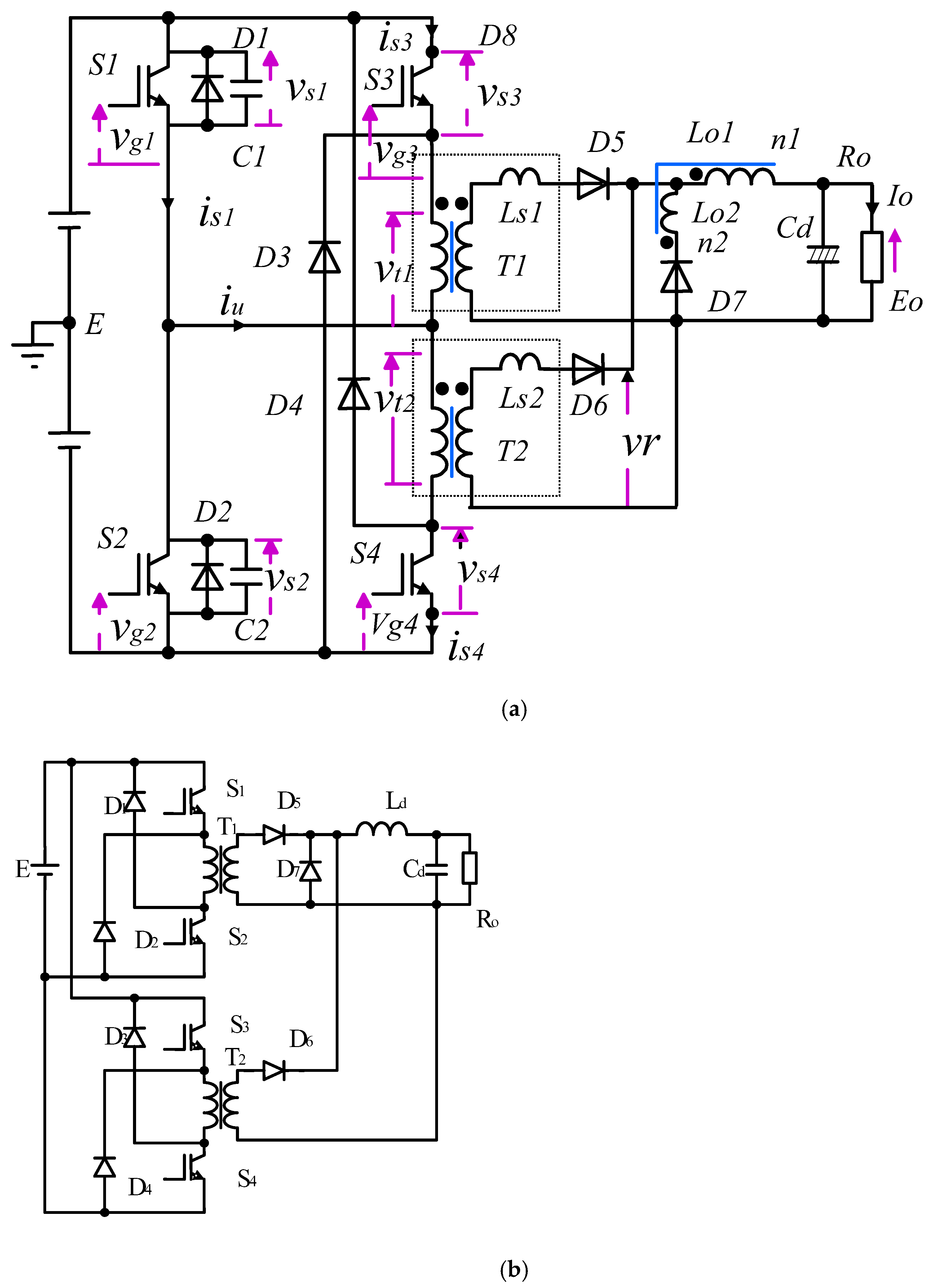
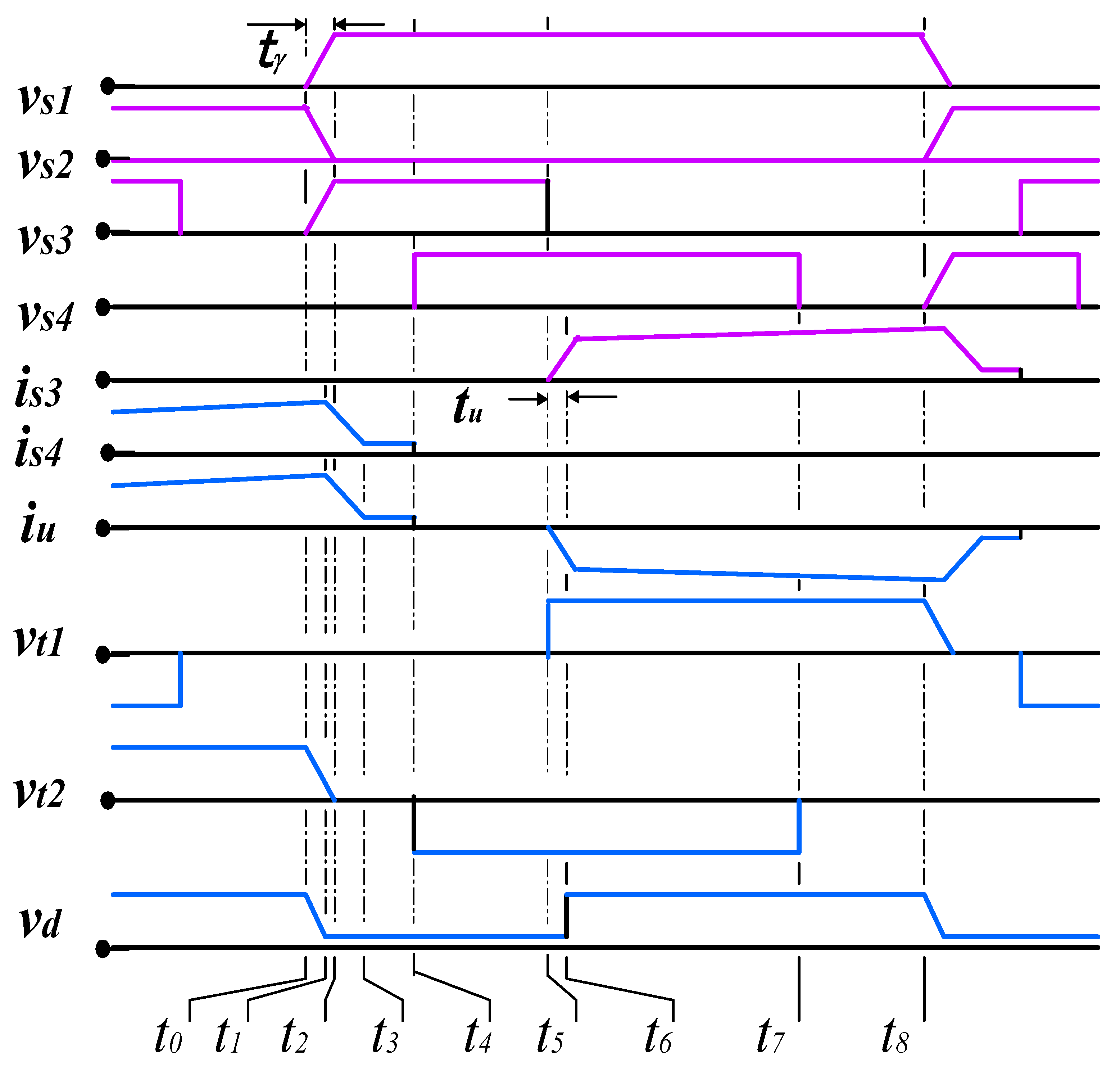
Figure 2 shows a basic circuit configuration of the proposed DC-DC power converter using the ultrafast IGBTs, which can work as a two-switch interleaving forward power converter with high frequency link. This circuit is a modified version of the two switch interleaved forward converter shown in Figure 2b. One of the forward-type power conversion stages composed of active power switches S1, S4, high frequency transformer T2, fast-recovery diodes D2, D4, and diode rectifier D6. The other bridge leg consists of active power switches S2, S3, high frequency transformer T1, fast recovery diodes D1, D3, and rectifier diode D5. Ls1 and Ls2 are low value leakage inductances of T1 and T2, correspondingly. A tapped inductor is used in the output stage as a low-pass filter. The gate pulse sequences and ideal waveforms of the power converter are demonstrated in Figure 3. The switching pulse sequences are different from those of the conventional interleaved two switch forward type power converter. Active power switch S4 (S3) is turned off after active power S1 (S2) is turned off with a short delay time tδ. Moreover, active power switches S1 and S2 are to be driven complementary with a short blanking interval td. The output voltage can be regulated by varying a controllable interval t α as PWM with a constant switching frequency. Figure 3 schematically shows the gate-pulse control signals of the S1, S2, S3 and S4 main switches of the proposed converter (Figure 2a). The well-known interleaving clocking method is illustrated in Figure 3. To interleave N parallel-connected (or series-connected) converter cells, active switches are switched at the same frequency as the switching operation, but pulses are phase-shifted by 2π/N radians [21].
The basic theory of operation under steady-state operating condition is described with the subsequent beliefs.
  • All the active power switches and passive power components are ideal.
  • High frequency transformers T1 and T2 are matching, so that every magnetizing and leakage inductances are characterized as Lp1 = Lp2 = Lp, Ls1 = Ls2 = Ls, respectively.
  • Capacitors C1 and C2 are identical: C1 = C2 = C.
  • Inductor Lo1 and Lo2 are coupled compactly and its coupling coefficient k ≈ 1.
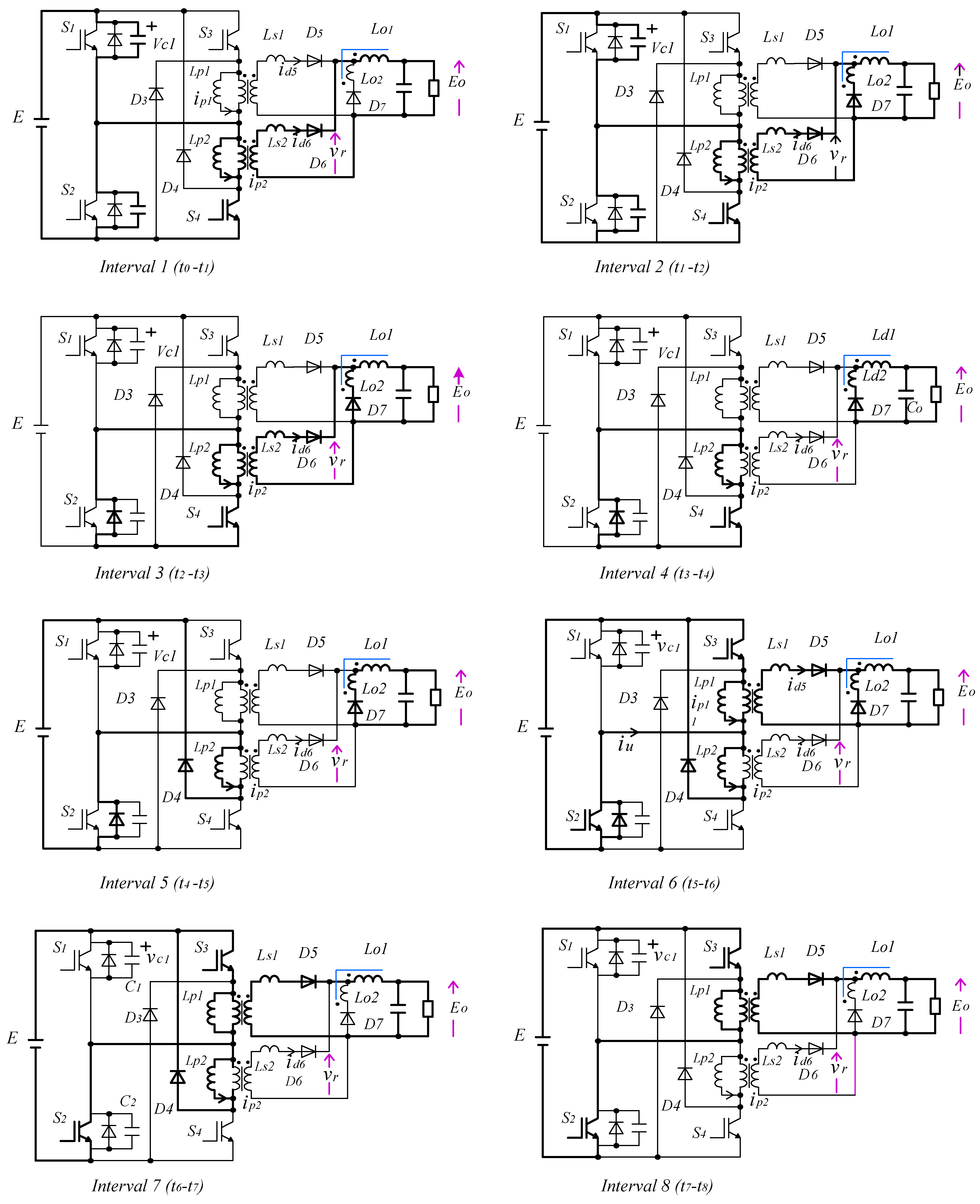
Figure 4 shows the operating current and voltage waveforms at each circuit components. Figure 5 depicts the topological equivalent circuits for one half-cycle interval in continuous conduction mode operation. Before time t 0 , active power switches S1, S4 and fast recovery rectifier diode D6 are conducting. Switching states equivalent circuits are done using the state of each switch and diode during one switching period. This method involves defining the set of states that the circuit enters in one period of operation. This method elaborates on the converter operation during one period, and corresponding equivalent circuits are given.
(a) Mode Interval 1 (t0t1): At time t 0 , active power switch S1 is turned off under zero voltage soft switching (ZVS) transition with the aid of lossless capacitive snubbers C1 and C2. Since inductances Lp and Ld1 are both large, magnetizing current ip2 and rectifier current id6 are to be assumed to be constant during this interval. Capacitor voltage vc1 increases, and rectified voltage vr decreases as:
v r = ( E v c 1 ) / N T
where NT is the turns ratio of the high-frequency transformer (NT = Np/Ns). Because Lo1 and Lo2 are coupled to each other compactly, freewheeling diode D7 starts conduction when vr reaches NL Eo. On the other hand, NL is the tapped-inductor turns ratio of the and is defined as N L = n 2 / ( n 1 + n 2 ) , n 1 and n 2 are the number of turns of Lo1 and Ld2, respectively.
(b) Mode Interval 2 (t1t2): The output current flows through D7, Lo2 and Lo1. Therefore, the output current reproduced to the primary side of the transformer drops. This interval ends when voltage vc2 goes down to zero.
(c) Interval 3 (t2t3): Diode D2 starts to conduct. The output current reflected to the transformer primary side continues to decrease. The current in capacitors C1 and C2 stops. Switch S4 is still conducting. The energy stored in Lp2 is transferring to the secondary side of HFT. However, this interval finishes when the current in diode rectifier id6 reaches zero.
(d) Interval 4 (t3–t4): The whole output current flows through D7, Lo2 and Lo1. The output current reflected to the transformer primary-side decreases to zero. This means no energy is transferring to the secondary side of HFT. Only a lesser magnetizing current of the transformer T2 circulates through transistor switch S4 and diode D2. This interval ends when the gate signal is removed from power switch S4. Therefore, S4 is turned off.
(e) Interval 5 (t4–t5): At time t4, corresponding to a delay time t δ , active power switch S4 is turned off under zero current soft-switching (ZCS). Magnetizing current ip2 flows through D2 and D4 to the DC voltage supply E as a resetting action of high frequency transformer T2. Then ip2 start decreasing. On the other hand, the load current still circulates through D7, Lo1 and Lo2.
(f) Interval 6 (t5–t6): At time t5, depending on duty-ratio of the power converter, S3 is turning-on under ZCS principle because the leakage inductance Ls1 make softer dis3/dt during turning-on operation of switch S3. Active power switch S2 is also turning-on with hybrid ZCS and ZVS transition when current iu becomes iu < 0. This is because diode D2 is conducting. The current in the primary-side of the HFT transformer flows through power switches S2 and S3. The current of magnetizing ip1 and rectifier current id5 starts circulation through switches S2 and S3, and diode D4. The energy is transferring to the secondary side of HFT through Ls1 and diode D5. During this period, the current is increasing in S3 and D5. Meanwhile, current iL2 through Ld2 reduces. This operation interval terminates when iL2 drops to zero.
(g) Operation interval 7(t6t7): At time t6, the diode D7 turns off. Therefore, the total output current streams through D5 and Ld1 while the magnetizing current ip2 continues decreasing with a constant slope -E/Lp.
(h) Interval 8 (t7t8): This interval starts at t7, the HFT magnetizing current ip2 drops to zero (t = t7), diode D4 as a passive switch turns off. The electrical energy is delivered to the load through S3, S2, T1 and D5. The half cycle operating intervals finish at time t8. The steady-state operation of the next half-cycle is similar to that of the discussed half-cycle. As mentioned above, S1 and S2 are turned-on and turned-off at ZVS soft-switching, while switches S3 and S4 behave with ZCS soft-switching at both turn-on and turn-off operation. The circulating and idling currents in both sides of high-frequency transformer HFT are considerably low with no supplementary auxiliary snubber circuits.

3. Steady State Operational Characteristics

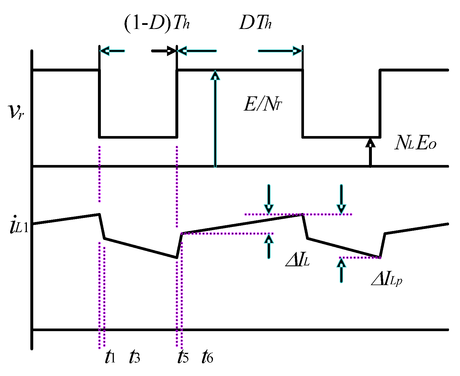
The output voltage characteristics and current stress on the active power switches are analytically estimated in continuous conduction mode in this section. Figure 6 depicts applicable waveforms of rectified voltage vr and the current through inductor iL1.
The output voltage is controlled by adjusting the duty cycle D when vr is high the current iL1 is increasing, when vr is low the current iL1 is decreasing until a new cycle comes. There are two filter inductors in series with the diode when current is delivered to the load to reduce the ripples in output currents. The output capacitor has to smooth out large pulsating output currents since it is supplied only during the switch OFF period.
This arrangement permits more favorable trapezoidal current waveforms and lower output current and voltage ripple, which consequently gives reduced noise and decreased stress on semiconductors and capacitors. Due to the non-pulsating characteristic of its output current, the forward converter is well suited for applications involving high output currents.
The peak current stress Isp for power switches S1S4 is given by
I s p = i p 2 ( t 1 ) + { i d 6 ( t 1 ) / N T }
and ip2(t1) is estimated as
i p 2 ( t 1 ) = D E T h / L p
where Th (Th = T/2) is the half-switching interval of the power converter, and D is the duty ratio of the power converter represented by D = (Th − Tα)/Th.
Since inductance Ls is significantly low, operational intervals from t1 to t3 and from t5 to t6 are small and negligible as depicted in Figure 6. Therefore, current i L 1 through Lo1 can be represented as,
{ n 1 i L 1 ( t 1 ) = ( n 1 + n 2 ) i L 1 ( t 3 ) ( n 1 + n 2 ) i L 1 ( t 5 ) = n 1 i L 1 ( t 6 ) .
Then, the current in diode id6(t1) and Δ I L p can be derived as
i d 6 ( t 1 ) = i L 1 ( t 1 ) = I o 1 ( 1 D ) N L + Δ I L 2
Δ I L p = N L I o 1 ( 1 D ) N L + ( 1 N L 2 ) Δ I L
where, I o is the output current and can be estimated by
I o = 1 T h 0 T h i L 1 ( t ) d t ,
and Δ I L = ( 1 D ) ( 1 N L ) E o T h / L d 1 .
Therefore, Isp is estimated by
I s p = D E T h L p + 1 N T { I o 1 ( 1 D ) N L + Δ I L 2 } .
The rectified voltage vr during a half cycle period can be represented as
v r = N L E o f o r t 1 < t t 6 v r = E f o r t 6 < t t 8 .
From Equation (9), the output voltage Eo can be derived as
E o = 1 T h 0 T h v d ( t ) d t         = D E N T { 1 ( 1 D ) N L } L s I o T h { 1 ( 1 D ) N L } 2 .
When leakage inductance Ls is small properly, the output voltage Eo is calculated as
E o D E N T { 1 ( 1 D ) N L }
Realizing Equations (8) and (10), when the HFT turns ratio NL is very small as NL << 1, both characteristics of output voltage and current stresses Isp are relatively similar to those of conventional hard-switched interleaving two switches DC-DC forward power converter. However, the main advantages of the interleaving scheme in forward DC-DC converters are reduced ripples in output and input capacitor currents. This enables flexible design to use smaller capacitor banks in input and output to satisfy output voltage ripple requirements. However, the peak currents in the converter circuit are reduced by a factor of two by using two output inductors which in turn decreases the EMI contents for these topologies. The size and cost of these power converters will reduce by reducing the size of filter capacitor banks.

4. Experimental Results and Discussions

This section presents a precise and concise explanation of the obtained experimental results, their analysis, as well as the experimental conclusions that can be presented. A prototype with power rating of 500 W (Eo = 50 V and output current Io = 10 A in experiment) 100 kHz breadboard using IGBTs is implemented in the laboratory to confirm the operating principle and validate the analytical steady state characteristics. The design specifications and the circuit parameters of this converter are designed as given in Table 1.
The inductance of magnetization and leakage inductance of the high frequency transformer are utilized for Lp1, Lp2 and Ls1, Ls2, respectively. The timing signal diagram of the power converter operating by means of a current mode control is illustrated in Figure 7. In order to continue operation with ZVS and ZCS soft-switching, a blanking time td and a delay time t δ are set to 0.5 μs and 0.7 μs, respectively.
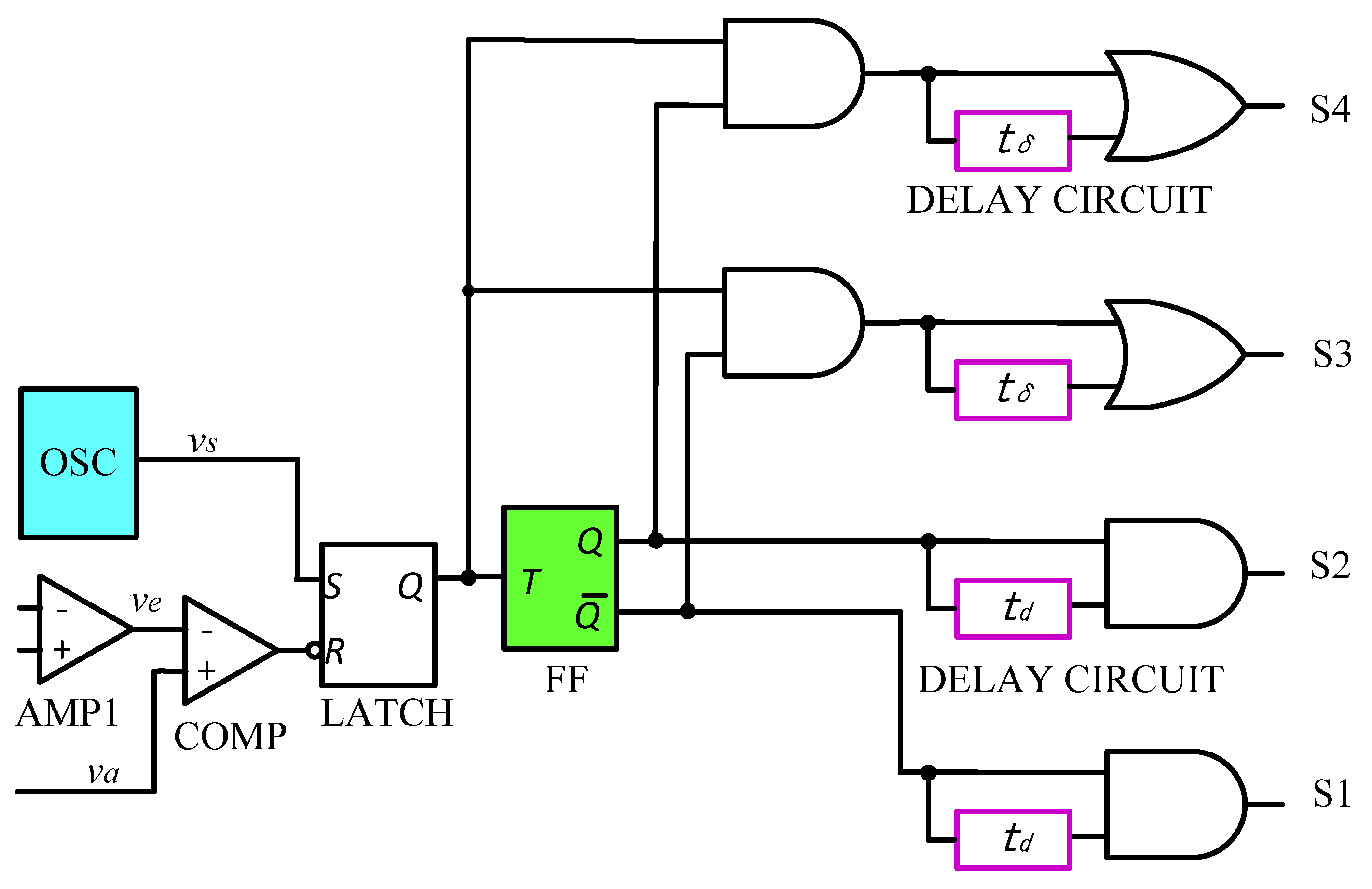
The basic timing principle elaborated in the generation of the gating signal is that the pulses generated should be able to turn ON only four semiconductor switches. A pulsed-latch is an ideal sequencing element for high-performance gate signals. The timing signal diagram of the power converter operating by means of a current mode control is implemented practically using the control circuit in Figure 8. The blanking time td and a delay time td are adjusted to continue operation with ZVS and ZCS soft-switching. The circuit composed of two op-amp comparators, latch, oscillator, S-R and T-flip-flops and delay.
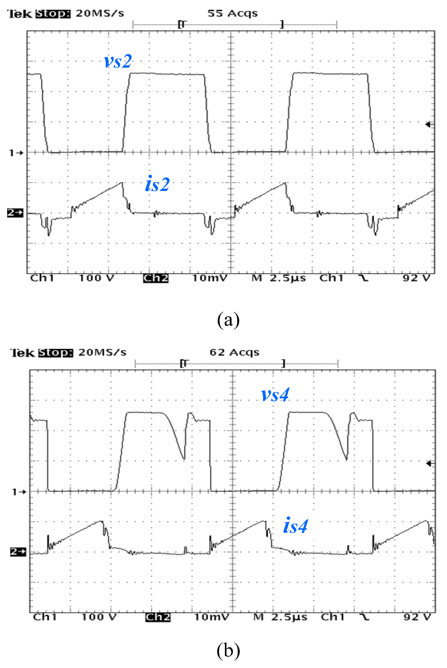
Figure 9 shows the voltage current characteristics of the new interleaved two-switches forward converter at Uin = 130 V. The duty cycle of the converter circuit is 0.3, 0.5 and 0.7. It can be seen that all the observed waveforms fit the theoretical analysis well. The experimental wave forms under reduced load with output current of 2 A are shown in Figure 10. The figure shows the switch voltage and current at the mentioned operating conditions. Figure 9 and Figure 10 depict observed voltages and currents waveforms under the specified conditions of E = 260 V, Eo = 50 V, Io = 10 A and E = 260 V, Eo = 50 V, Io = 2 A. In both cases, active semiconductor devices S1 and S2 operate achieving ZVS soft-switching, and active power switches S3 and S4 operate achieving ZCS soft-switching at turn-on and turn-off by realizing low idling and circulation currents.
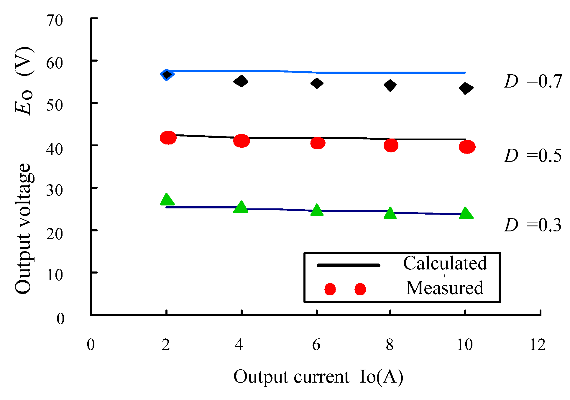
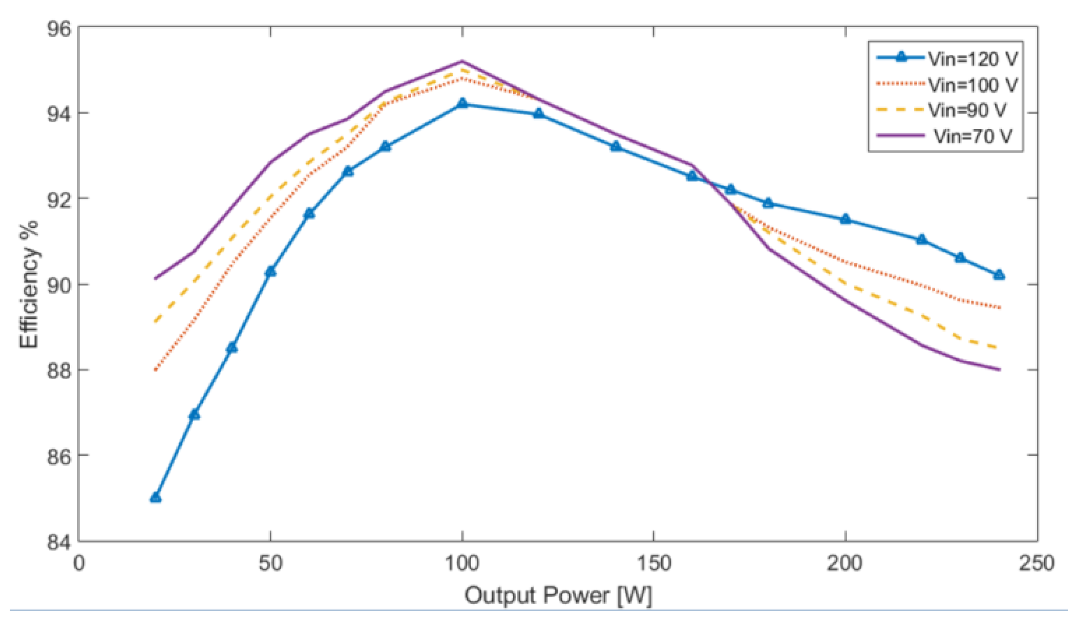
The output voltage is calculated by Equation (10). The measured and calculated output voltages are plotted versus output current characteristics and shown in Figure 11. The duty cycle is taken as a parameter under using open loop control scheme. One can observe that the reduction of the converter output voltage produced by the existence of leakage inductance Ls is noticeably low. The actual measured efficiency is shown in Figure 12 as a function of the output load current in case of constant output voltage equal to 50 V. The achieved power conversion efficiency is equal to 93.5% during full-load operating condition.

5. Discussion

In this section, the results are discussed and how they can be interpreted from the perspective of previous studies and of the working hypotheses. The efficiency variation with the output power at different voltages is shown in Figure 12. The measured efficiencies of the proposed converter are evaluated at different input voltages (70 V, 90 V, 110 V and 130 V). The tested results indicate the benefits of the unique architecture. High energy efficiency over wide input voltage range is achieved. Table 2 shows the calculated voltage and current stresses appear during operation for each power converter. A comparative evaluation is made for voltage and current stresses of the implemented converter from a practical point of view. However, the output voltage reduction caused by the forward voltage dropping on the active power switches and diodes, and the effective duty cycle decrease due to the leakage inductances of the high-frequency transformer HFT are approximately assessed totally as 3 V. Although the current ripple of output inductor in the studied DC-DC power converter is pretty considerable, the RMS current stresses on the inductor and the active power switches are nearly the same as compared with those of the hard-switching DC-DC power converter. The experimental results take conduction power losses of the implemented soft-switched DC-DC power converter as low as those of the hard-switched DC-DC power converter.
Figure 13 shows efficiency comparison for the new and conventional interleaved forward power converter in case of 130 V input voltage. It seems that the higher the output power, the lower the efficiency. It is because the conduction losses are the major parts of total losses. All the parameters and devices of the two forward converters are the same except that the resistors RC1 and RC2 in the conventional forward converter are 510 Ω. It is obvious that the new converter can achieve higher conversion efficiency compared with the conventional one, because most of the magnetizing and leakage energy of the transformer is recycled.
References [21,22,23,24] proposed a series of schemes to improve the performance of two-switch forward converter. Among them, references [40,41,42] have the functions of improving duty cycle and soft switching. However, all of them used auxiliary switches, which will increase the complexity of the topology. In addition, these topologies generally have high voltage stress problem in switches.
Table 3 gives a comparison between the proposed and previous circuits in terms of rating and voltage stresses on switches.

6. Conclusions

A soft-switched two switch interleaved forward PWM DC-DC power converter using ultrafast IGBTs has been presented as a new generation converter topology in this paper for telecommunication plants. Its operating principle of this converter has been verified with steady-state analysis and experimentally tested by 500 W–100 kHz breadboard using ultrafast IGBTs. The proposed soft-switched PWM-DC-DC converter circuit is characterized by the following exceptional characteristics:
  • The switching losses are low through a wide-ranging of load variation.
  • Circulating currents are low, resulting in a low amount of conduction losses.
  • No need for using additional auxiliary snubber circuits.
  • No existence of flux imbalance in the two high frequency transformer windings because of the existence of forward configuration of the converter.
Compared with the bridge converter, the two-switch forward converter has many advantages, such as simple structure, high stability, and simple magnetic reset method. Thus, it is very suitable for high reliability applications. The transformer in the forward converter can only excite in one direction, which means its core volume is larger than that of the bridge converter. However, in a high frequency working environment, it is the thermal stress produced by core loss, rather than the saturated flux density, that plays a major role in constraining the flux swing. Therefore, in a high frequency environment, the problem of the forward converter core size increasing is eliminated.
In the future, the transient analysis of this converter should be assessed from an experimental point of view.

Author Contributions

Conceptualization, K.S. and A.G.A.-K.; methodology, K.S.; software, K.S.; validation, A.G.A.-K. and K.S.; formal analysis, K.S.; investigation, A.G.A.-K.; resources, A.G.A.-K.; data curation, K.S.; writing—review and editing, writing—original draft preparation, K.S. and A.G.A.-K.; visualization, K.S.; supervision, K.S.; All authors have read and agreed to the published version of the manuscript.

Funding

This research received no external funding.

Data Availability Statement

The data that support the findings of this study are available on request from the authors.

Conflicts of Interest

The authors declare no conflict of interest.

References

  1. Sayed, K. ZVS Soft-Switched DC-DC Converter based Charger for Low Voltage battery in Hybrid Electric Vehicles. IET Power Electron. 2019, 12, 3389–3396. [Google Scholar] [CrossRef]
  2. Sayed, K.; Kwon, S.K.; Nishida, K.; Nakaoka, M. New DC Rail Side Soft-Switching PWM DC–DC Converter with Current Doubler Rectifier. In Proceedings of the IEEE Ninth International Conference Power Electronics and Drive Systems (PEDS), Singapore, 5–8 December 2011; pp. 687–694. [Google Scholar]
  3. Sayed, K.; Kwon, S.K.; Nishida, K.; Nakaoka, M. New DC Rail Side Soft-Switching PWM DC–DC Converter with Voltage Doubler Rectifier for PV Generation Interface. In Proceedings of the IEEE International Power Electronics Conference (IPEC—ECCE-ASIA), Hiroshima, Japan, 18–21 May 2014; pp. 2359–2365. [Google Scholar]
  4. Ashraf, N.; Izhar, T.; Abbas, G.; Awan, A.B.; Alghamdi, A.S.; Abo-Khalil, A.G.; Sayed, K.; Farooq, U.; Balas, V.E. A New Single-Phase Direct Frequency Controller Having Reduced Switching Count without Zero-Crossing Detector for Induction Heating System. Electronics 2020, 9, 430. [Google Scholar] [CrossRef]
  5. Saleeb, H.; Sayed, K.; Kassem, A.; Mostafa, R. Control and analysis of bidirectional interleaved hybrid converter with coupled inductors for electric vehicle applications. Electr. Eng. 2020, 102, 195–222. [Google Scholar] [CrossRef]
  6. Hamada, S.; Nakaoka, M. A Novel Zero-Voltage and Zero-Current Switching PWM DC-DC Converter with Reduced Conduction Losses. IEEE Trans. Power Electron. 2002, 17, 413–419. [Google Scholar] [CrossRef]
  7. Sayed, K.; Almutairi, N.; Albagami, N.; Alrumayh, O.; Abo-Khalil, A.G.; Saleeb, H. A Review of DC-AC Converters for Electric Vehicle Applications. Energies 2022, 15, 1241. [Google Scholar] [CrossRef]
  8. Kim, E.S.; Joe, K.Y.; Kye, M.H.; Kim, Y.H.; Yoon, B.D. An improved soft-switching PWM FB DC/DC converter for reducing conduction losses. IEEE Trans. Power Electron. 1999, 14, 258–263. [Google Scholar]
  9. Sayed, K.; Abo-Khalil, A.G.S.; Alghamdi, A. Optimum Resilient Operation and Control DC Microgrid Based Electric Vehicles Charging Station Powered by Renewable Energy Sources. Energies 2019, 12, 4240. [Google Scholar] [CrossRef]
  10. Saleeb, H.; Sayed, K.; Kassem, A.; Mostafa, R. Power Management Strategy for Battery Electric Vehicles. IET Electr. Syst. Transp. 2019, 9, 65–74. [Google Scholar] [CrossRef]
  11. Almutairi, A.; Sayed, K.; Albagami, N.; Abo-Khalil, A.G.; Saleeb, H. Multi-Port PWM DC-DC Power Converter for Renewable Energy Applications. Energies 2021, 14, 3490. [Google Scholar] [CrossRef]
  12. Wu, H.; Xing, Y. Families of Forward Converters Suitable for Wide Input Voltage Range Applications. IEEE Trans. Power Electron. 2014, 29, 6006–6017. [Google Scholar] [CrossRef]
  13. O’Loughlin, M. 200-W Interleaved Forward Converter Design Review Using TI’s UCC28221 PWM Controller; Texas Instruments: Dallas, TX, USA, 2004. [Google Scholar]
  14. Park, K.B.; Moon, G.W.; Youn, M.J. Series-input series-rectifier interleaved forward converter with a common transformer reset circuit for high-input-voltage applications. IEEE Trans. Power Electron. 2011, 26, 3242–3253. [Google Scholar] [CrossRef]
  15. Park, K.B.; Moon, G.W.; Youn, M.J. Three-switch active-clamp forward converter with low voltage stresss and wide ZVS range for high-input-voltage applications. IEEE Trans. Power Electron. 2010, 25, 889–898. [Google Scholar] [CrossRef]
  16. Eshkevari, A.L.; Mosallanejad, A.; Sepasian, M. Design, modelling, and implementation of a modified double-switch flyback-forward converter for low power applications. IET Power Electron. 2019, 12, 739–748. [Google Scholar] [CrossRef]
  17. Lin, B.R.; Chiang, H.K. Analysis and implementation of a soft switching interleaved forward converter with current doubler rectifier. IET Electr. Power Appl. 2007, 1, 697–704. [Google Scholar] [CrossRef]
  18. Wu, H.; Xu, P.; Liu, W.; Xing, Y. Series-Input Interleaved Forward Converter With a Shared Switching Leg for Wide Input Voltage Range Applications. IEEE Trans. Ind. Electron. 2013, 60, 5029–5039. [Google Scholar] [CrossRef]
  19. Musumeci, S.; Stella, F.; Mandrile, F.; Armando, E.; Fratta, A. Soft-Switching Full-Bridge Topology with AC Distribution Solution in Power Converters’ Auxiliary Power Supplies. Electronics 2022, 11, 884. [Google Scholar] [CrossRef]
  20. Lin, B.R.; Shih, H.Y. Implementation of a parallel zero-voltage switching forward converter with less power switches. IET Power Electron. 2011, 4, 248–256. [Google Scholar] [CrossRef]
  21. Gu, Y.; Lu, Z.; Qian, Z.; Gu, X.; Hang, L. A novel ZVS resonant reset dual switch forward DC-DC converter. IEEE Trans. Power Electron. 2007, 22, 96–103. [Google Scholar] [CrossRef]
  22. Kim, J.K.; Choi, S.W.; Moon, G.W. Zero-voltage switching postregulation scheme for multioutput forward converter with synchronous switches. IEEE Trans. Ind. Electron. 2011, 58, 2378–2386. [Google Scholar] [CrossRef]
  23. Shi, K.; Zhang, D.; Gu, Y. Interleaved Current-Driven Phase-Shift Full-Bridge Converter with Magnetic Integration and Voltage Doubler Rectifiers. IEEE Trans. Power Electron. 2018, 33, 8308–8321. [Google Scholar] [CrossRef]
  24. Chu, E.; Bao, J.; Xie, H.; Hui, G. A Zero-Voltage and Zero-current Switching Interleaved Two-Switch Forward Converter with Passive Auxiliary Resonant Circuit. IEEE Trans. Power Electron. 2019, 35, 4859–4876. [Google Scholar] [CrossRef]
  25. Qin, W.; Wu, X.; Zhang, J. A Family of DC Transformer (DCX) Topologies Based on New ZVZCS Cells with DC Resonant Capacitance. IEEE Trans. Power Electron. 2017, 32, 2822–2834. [Google Scholar] [CrossRef]
  26. Li, W.; Fan, L.; Zhao, Y.; He, X.; Xu, D.; Wu, B. High-Step-Up and High-Efficiency Fuel-Cell Power-Generation System with Active-Clamp Flyback–Forward Converter. IEEE Trans. Ind. Electron. 2012, 59, 599–610. [Google Scholar]
  27. Lipu, M.S.H.; Faisal, M.; Ansari, S.; Hannan, M.A.; Karim, T.F.; Ayob, A.; Hussain, A.; Miah, M.S.; Saad, M.H.M. Review of Electric Vehicle Converter Configurations, Control Schemes and Optimizations: Challenges and Suggestions. Electronics 2021, 10, 477. [Google Scholar] [CrossRef]
  28. Saleeb, H.; Kassem, R.; Sayed, K. Artificial neural networks applied on induction motor drive for an electric vehicle propulsion system. Electr. Eng. 2022, 104, 1769–1780. [Google Scholar] [CrossRef]
  29. Sayed, K.; Ali, Z.M.; Aldhaifallah, M. Phase-shift PWM-controlled DC–DC converter with secondary-side current doubler rectifier for on-board charger application. Energies 2020, 13, 2298. [Google Scholar] [CrossRef]
  30. Sayed, K.; Gronfula, M.G.; Ziedan, H.A. Novel Soft-Switching Integrated Boost DC-DC Converter for PV Power System. Energies 2020, 13, 749. [Google Scholar] [CrossRef]
  31. Jin, T.; Zhang, K.; Zhang, K.; Smedley, K. A New Interleaved Series Input Parallel Output (ISIPO) Forward Converter with Inherent Demagnetizing Features. IEEE Trans. Power Electron. 2008, 23, 888–895. [Google Scholar] [CrossRef]
  32. Khorasani, R.R.; Adib, E.; Farzanehfard, H. ZVT Resonant Core Reset Forward Converter with a Simple Auxiliary Circuit. IEEE Trans. Ind. Electron. 2018, 65, 242–250. [Google Scholar] [CrossRef]
  33. Qian, T.; Wu, Q. A Scheme of a Resonant Forward-Flyback Converter with Suppressed Frequency Variation. IEEE Trans. Power Electron. 2018, 33, 3711–3716. [Google Scholar] [CrossRef]
  34. Sayed, K.; Gabbar, H.A. Electric Vehicle to Power Grid Integration Using Three-Phase Three-Level AC/DC Converter and PI-Fuzzy Controller. Energies 2016, 9, 532. [Google Scholar] [CrossRef]
  35. Wu, H.; Xing, Y. A Family of Forward Converters with Inherent Demagnetizing Features Based on Basic Forward Cells. IEEE Trans. Power Electron. 2010, 25, 2828–2834. [Google Scholar] [CrossRef]
  36. Dias, C.D.P.; Pereira, A.A.; Farias, V.J.; Vieira, J.B.; de Freitas, L.C. An improved self-resonant PWM forward converter. IEEE Trans. Power Electron. 2000, 15, 479–484. [Google Scholar] [CrossRef]
  37. Dasohari, M.; Neti, V.; Porpandiselvi, S.; Manikyavani, A.R. An Interleaved Dual Double-Ended Forward Converter Based LED Driver for DC Lighting Grids. In Proceedings of the 2020 21st National Power Systems Conference (NPSC), Gandhinagar, India, 17–19 December 2020; pp. 1–5. [Google Scholar] [CrossRef]
  38. Matsushita, Y.; Noguchi, T.; Taguchi, N.; Ishii, M. 2 kW Dual-Output Isolated DC/DC Converter Based on Current Doubler and Step-Down Chopper. World Electr. Veh. J. 2020, 11, 78. [Google Scholar] [CrossRef]
  39. Ezra, N.; Werner, T.; Long, T. Dual Voltage Forward Topology for High Efficiency at Universal Mains. Electronics 2022, 11, 1009. [Google Scholar] [CrossRef]
  40. Arazi, M.; Payman, A.; Camara, M.B.; Dakyo, B. Bidirectional Interface Resonant Converter for Wide Voltage Range Storage Applications. Sustainability 2022, 14, 377. [Google Scholar] [CrossRef]
  41. Taheri, M.; Milimonfared, J.; Bayat, H.; Riazmontazer, H.; Noroozi, A. Analysis and Design of a New Choke Less Interleaved ZVS Forward-Flyback Converter. In Proceedings of the 2011 2nd Power Electronics, Drive Systems and Technologies Conference, Tehran, Iran, 16–17 February 2011; pp. 81–86. [Google Scholar] [CrossRef]
  42. Kim, H.S.; Seong, H.W.; Park, K.B.; Youn, H.S.; Moon, G.W.; Youn, M.J. Zero-Voltage-Switching Interleaved Two-Switch Forward Converter with Phase-Shift Control. In Proceedings of the IEEE Energy Conversion Congress and Exposition, Atlanta, GA, USA, 12–16 September 2010; pp. 3727–3732. [Google Scholar]
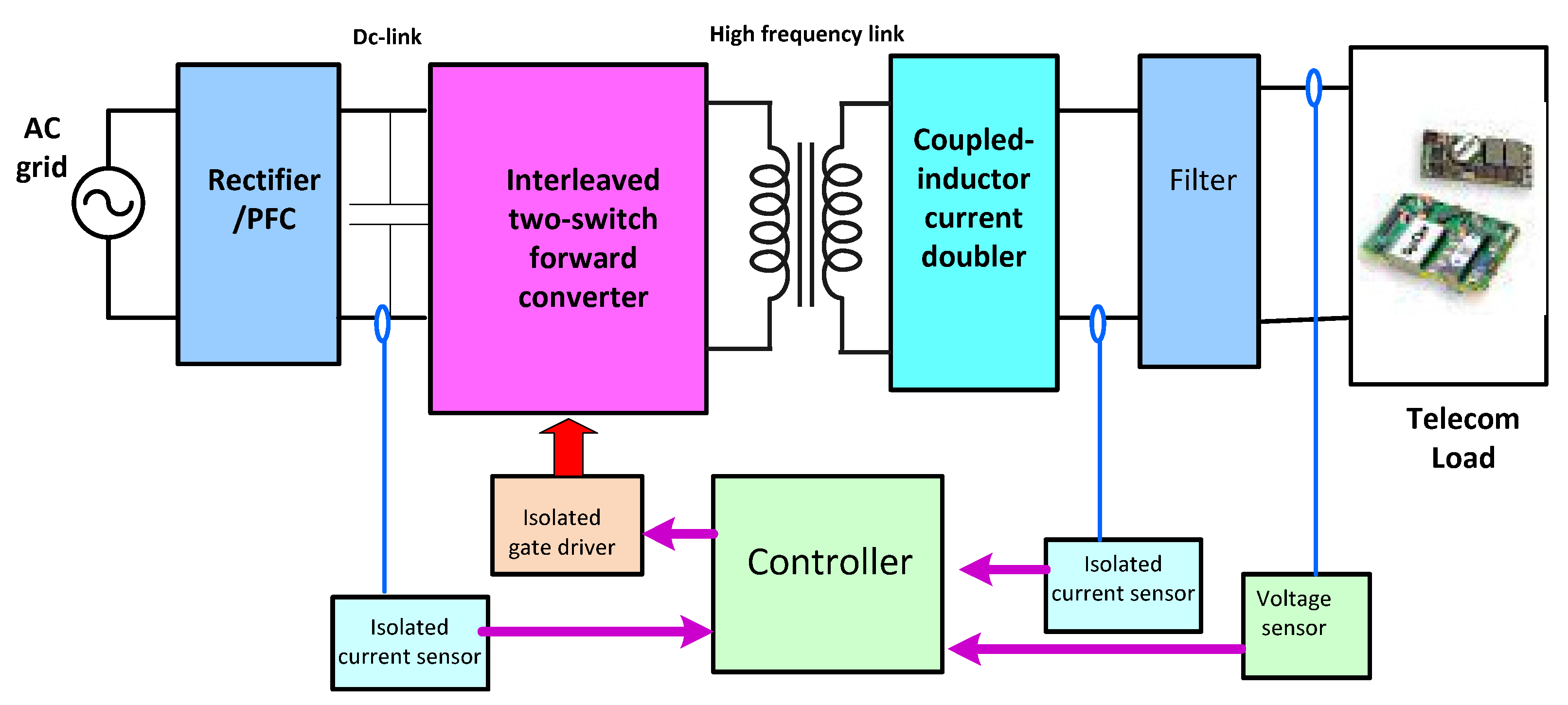
Figure 1. Basic building blocks of the proposed converter.
Electronics 11 02551 g001
Figure 2. (a) Basic circuit configuration of the studied converter. (b) Two-switch interleaved hard-switched forward DC-DC converter.
Electronics 11 02551 g002
Figure 3. Gate voltage pulse sequences.
Electronics 11 02551 g003
Figure 4. Typical operating waveforms of studied DC-DC power converter.
Electronics 11 02551 g004
Figure 5. Equivalent circuits of the circuit during half cycle operating intervals.
Electronics 11 02551 g005
Figure 6. Rectified voltage vr and inductor current iL1 operational waveforms.
Electronics 11 02551 g006
Figure 7. Timing diagram of the controller.
Electronics 11 02551 g007
Figure 8. Generation of gate signal for power switches.
Electronics 11 02551 g008
Figure 9. Experiment waveforms of the prototype at E = 260 V, Eo = 50 V, Io = 10 A. (vs.: 100 V/div., is: 2 A/div., time scale: 2.5 µs/div). (a) Switch S2 current and voltage (b) Switch S4 current and voltage.
Electronics 11 02551 g009
Figure 10. Experiment waveforms of the prototype at E = 260 V, Eo = 50 V, Io = 2 A. (vs.: 100 V/div., is: 2 A/div., time scale: 2.5 µs/div). (a) Switch S2 current and voltage (b) Switch S4 current and voltage.
Electronics 11 02551 g010
Figure 11. Calculated and measured output voltages versus load current.
Electronics 11 02551 g011
Figure 12. Measured output power at different input voltages.
Electronics 11 02551 g012
Figure 13. Efficiency comparison between the conventional and developed converter.
Electronics 11 02551 g013
Table 1. Circuit parameters of prototype converter.
S1S4IRG4PC40W
Vces = 600 V, Ic = 20 A(Tc = 100 °C),
Coes = 140 pF (at Vcc = 30 V)
D1D4:SF8L60, VRRM = 600 V, IF = 8 A
D5D7:ESAC93M-03, VRRM = 300 V, IF = 12 A
C1, C2820 pF (parallel connected with S1 and S2.)
T1, T2:Np = 23 Turns, Ns = 7 Turns, N T = 3.3
Lp1, Lp2:2.5 mH (HFT Magnetizing inductance)
Ls1, Ls2:0.35 μH (HFT Leakage inductance)
Lo1, Lo2Lo1 = 35 μH, Lo2 = 1.1 μH, NL = 0.14, k = 0.933
Co540 μF
Table 2. Comparison of voltage and current stresses of the proposed and conventional converter.
Conventional Hard-Switching
Converter
Proposed Soft-Switching
Converter
Input parameters. E min = 220   V , E = 260   V , E o = 53   V , I o = 10   A , f s = 100   kHz , D max = 0.8 , L d = 35   μ H . E min = 220   V , E = 260   V , E o = 53   V , I o = 10   A ,
f s = 100   kHz , D max = 0.8 , L d 1 = 35   μ H , N L = 0.14 .
Turns ratio of the
HFT transformer.
N T = D max E min E o 3.32 N T = D max E min { 1 ( 1 D max ) N L } E o 3.42
Duty cycle under rated voltage operation E. D = N T E o E 0.677 D = ( 1 N L ) N T E o E N T N L E o 0.664
Current ripple in the output inductor (peak-to-peak ripple). Δ I L P = ( 1 D ) E o T h L d 1 2.45 A Δ I L P = N L I o 1 ( 1 D ) N L + ( 1 N L 2 ) Δ I L 3.51 A
Output inductor RMS current. I L r m s = I o 10.0 A I L 1 r m s = I o D + ( 1 D ) ( 1 N L ) 2 1 ( 1 D ) N L 10.0 A
Peak current through active power switches. I S P = 1 N T { I o + Δ I L p 2 } 3.38 A I S P = 1 N T { I o 1 ( 1 D ) N L + Δ I L 2 } 3.39 A
Average current through the active power switches. I S A V = D I o 2 N T 1.02 A I S A V = 1 2 N T { D I o 1 ( 1 D ) N L } 1.02 A
RMS current through active power switches. I S = D I o 2 N T 1.75 A I S = 1 2 N T { D I o 1 ( 1 D ) N L } 1.77 A
Peak voltage on the active power switches. V S P = E 260 V V S P = E 260 V
Table 3. Comparison between the proposed and previous.
Paper [24]Paper [21][42][6]Proposed
Input voltage E260250–400320–400260220–260
Output voltage Vo5054485053
Output current10 A5 A10 A10 A10 A
Switching frequency fs100 kHz100100 kHz100 kHz100 kHz
NT Turns ratio3.5:150:2060:1023:7:3.323:7:7
Voltage stress S1S4
D5D6
E
E/NT-Vo
E
2E/NT
E
2E/NT
E
2E/NT
E
E/NT-Vo
Publisher’s Note: MDPI stays neutral with regard to jurisdictional claims in published maps and institutional affiliations.