2.1. Power Losses of Push–Pull Converter
The overall converter efficiency is defined as:
where
PIN stands for input power,
POUT represents output power, and
PLOSS covers total power losses in the converter. Clearly, the efficiency can be easily derived from (1) if we know how to calculate total power losses.
As given in [
23], the total power losses
PLOSS can be expressed as:
where:
PCOND—conduction losses,
PFIXED—fixed losses,
WTOT—total energy consumed during one period. Average dynamic power losses can be represented as
PDYN =
WTOT·
fsw. Clearly, the dynamic losses directly depend on switching frequency
fsw. On the other end, controller power supply current and leakage currents contribute to fixed losses. They are negligible in comparison to conduction and dynamic losses and, therefore, can be excluded from further analysis.
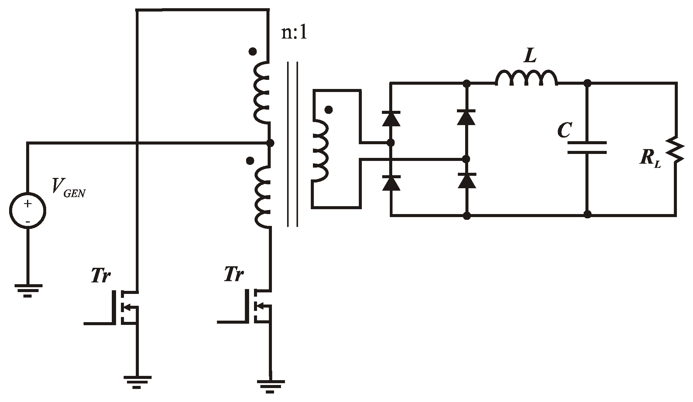
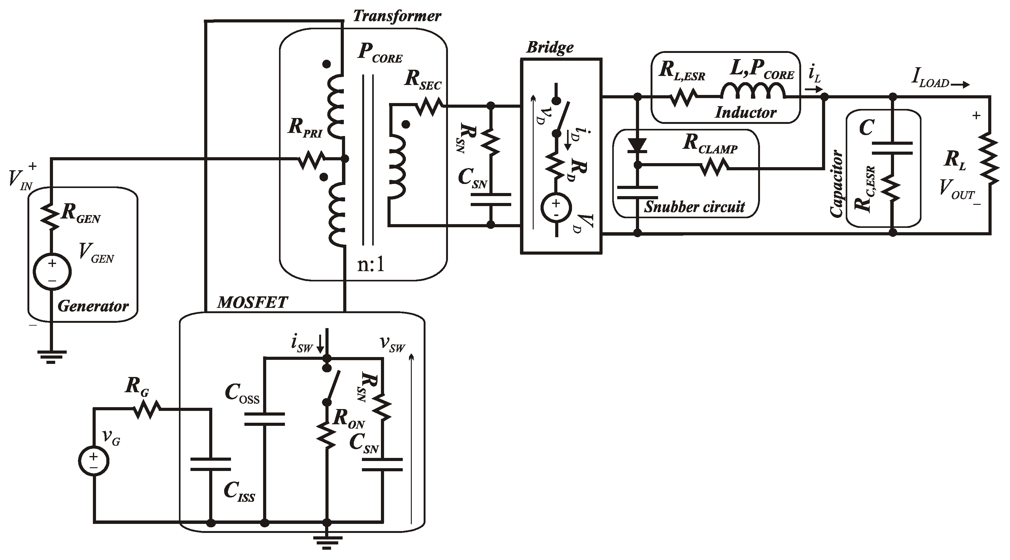
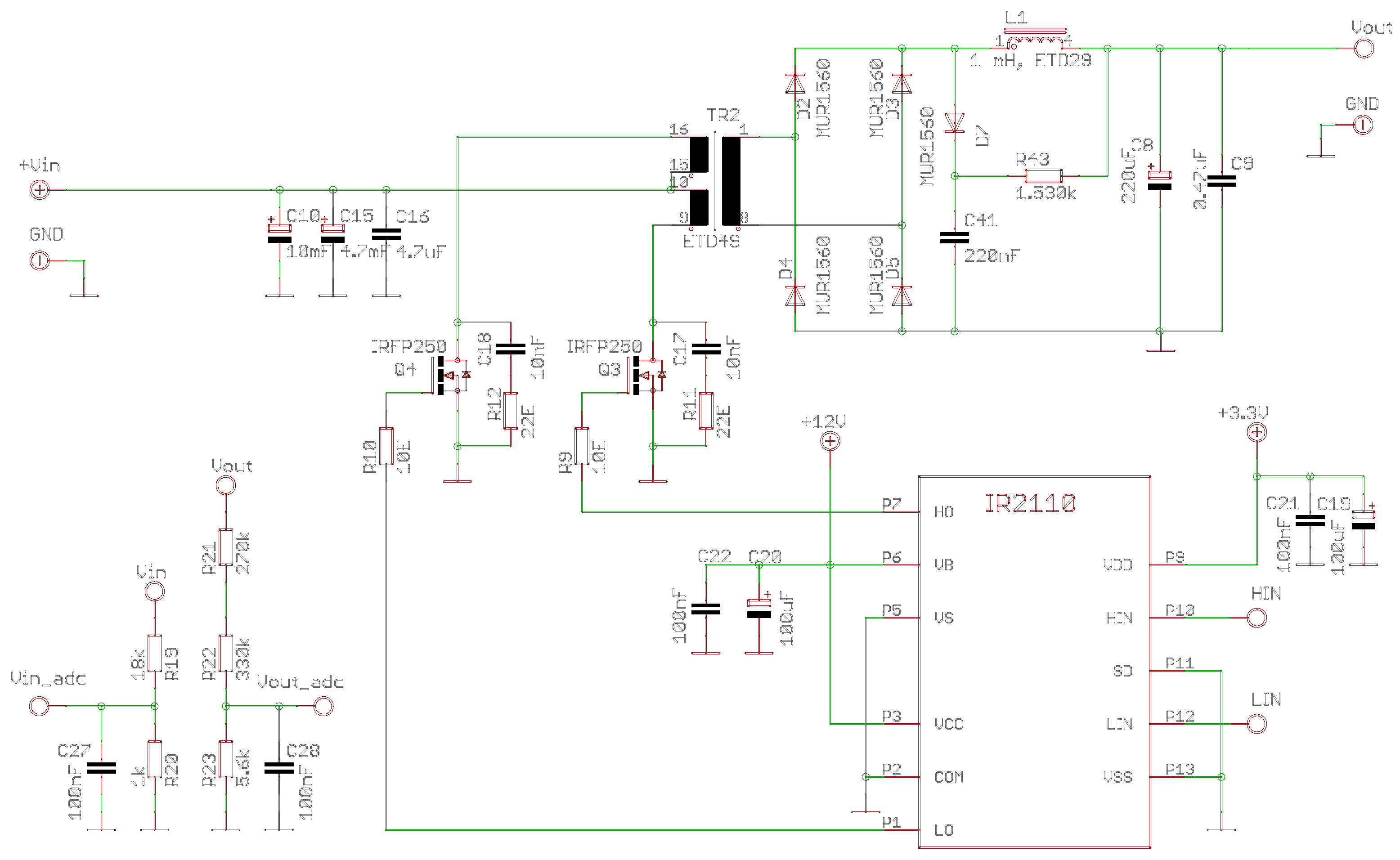
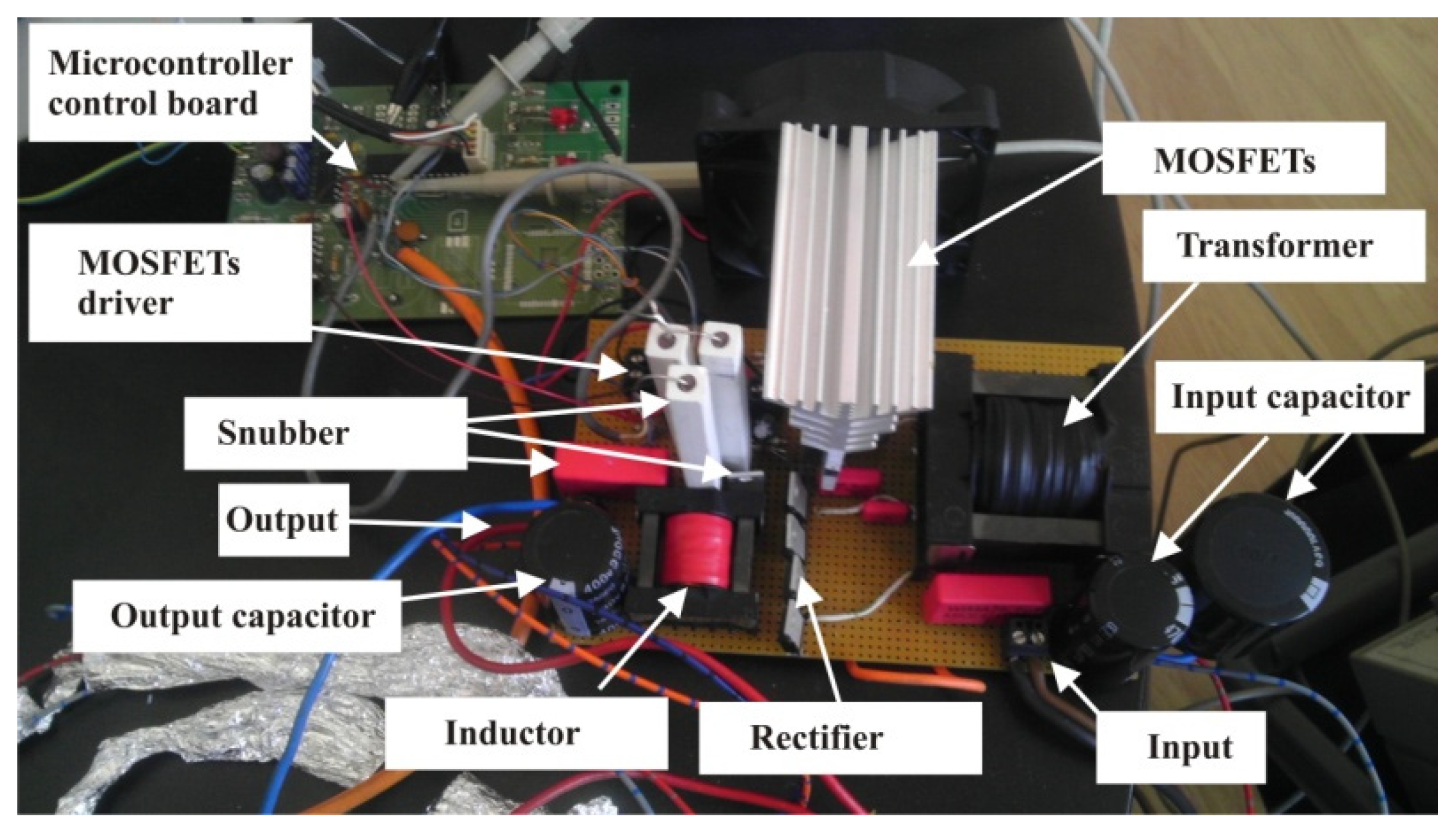
Equivalent circuit of the push–pull converter, including the parasitic elements, is depicted in
Figure 2. When MOSFET is used as a switching element, it can be modeled with
RON (when turned on). The model also includes the transistor input capacitance
CISS. Diode (forward-biased) is modeled using constant voltage source
VD and resistance
RD.
The equivalent circuit also includes power losses on
RC,ESR (equivalent series resistance of the output filter capacitance). Similarly, inductor equivalent series resistance (
RL,ESR) accounts for its conduction losses. In addition, we consider inductor core power losses. Finally, the supply circuit is modeled as a series of resistance
RGEN and voltage generators, where
RGEN represents converter supply circuit losses. In [
23], an analytical expression is given for
RGEN for the case when the supply circuit consists of AC generator and single-phase or three-phase rectifier.
Conduction losses of push–pull converter can be calculated using the following equation:
where
ISW,eff,
ID,eff,
IC,eff,
IIN,eff represent effective values of currents through switch, diode, output capacitor and converter input, respectively.
ID,avg is average diode current.
PL,COND and
PTR,COND are conduction losses in inductor and transformer windings, respectively.
PCLAMP is power dissipation of the limiting circuit of the rectifier output.
The currents through inductor and transformer have periodic non-sinusoidal waveform. In that regard, we can separately analyze conduction losses in the windings caused by DC and AC currents [
24]. For both CCM and DCM operating modes, it can be assumed that the amplitude of the fundamental harmonic prevails when compared with other harmonics. Therefore, we can safely confine the winding conduction losses caused by AC inductor current to power losses of the fundamental harmonic. Given all above, overall conduction losses are approximated as
Here, RL,ESRL,DC represents inductor equivalent serial resistance for DC current. The second term in (4) accounts for power losses in the winding due to the skin and proximity effects, where RL,ESR,AC denotes inductor resistance for the AC current I1L,EFF at the switching frequency.
By using the equation for effective value of periodic non-sinusoidal signals, we approximate the inductor effective current for the fundamental harmonic as
Furthermore,
RL,ESR,AC is given by the following Equation [
25]:
where
m stands for number of layers of the inductor winding and
RDC,m represents resistance of the
mth layer for DC current
In the equation above,
ρ is resistivity of the wire,
Nm number of turns in the
mth layer,
lm,turn one turn wire length, and
AW is the wire cross-sectional area. Moreover,
ξ from (6) is characterized as
where
d represents the diameter of the wire and
δ stands for skin depth, which can be calculated as
where
μ is wire permeability.
The power dissipation of the limiting circuit of the rectifier output can be determined by:
where
VSEC is voltage amplitude on transformer’s secondary winding.
Total dynamic power losses of push–pull converter are calculated as:
where:
PISS is power loss in transistor gate,
PSW is power loss during switching,
PBRIDGE is power loss in rectifier,
PL,CORE is dynamic power loss in inductor core,
PTR,CORE is dynamic power loss in transformer core,
PSW,SNUB is power loss in snubber circuit of the switch, and
PSEC,SNUB is power loss in snubber circuit of the transformer’s secondary winding. We note here that, in the case of push–pull converter, if snubber circuit is used on the transformer’s secondary winding, then limiting circuit is not used and vice versa.
Switch gate power losses are expressed as [
26]:
where
QG is total charge in the gate and
VCG is supply voltage of gate control circuit.
In the case of MOSFET, the power losses come up when the switches transit between the states and is given by
where
tvr and
tvf are rising and falling time of the output voltage, respectively. Factor
k is between 1/6 and 1/2 [
27]. Rising and falling times can be calculated using the equations from [
16]:
Here,
QG (SW) represents gate charge at the switching point, which can be expressed with the following equation:
The MOSFET gate currents, when transistor turns on and off, are, respectively, given by
where
VSP,ON and
VSP,OFF are voltages at the switching points. The values of these voltages can be retrieved from the gate charge diagram from the MOSFET specifications. Alternatively, they can be calculated approximately with equations:
Here, VG represents gate threshold voltage, and gm stands for MOSFET transconductance.
Normally, dynamic losses contain power losses caused by the discharging process of the switching element (MOSFET) output capacitance
COSS. However, the authors in [
17] proved that they are already expressed in (13).
Dynamic power losses in rectifier can be calculated as:
where:
VSEC-secondary voltage,
trr-diode recovery time,
Qr-pn junction accumulated charge. The losses in (21) are present only when the converter operates in CCM. Given that the diode current is zero when transistor turns on, we can conclude that these losses are zero in DCM.
The losses in inductor and transformer cores originate from hysteresis and eddy currents. According to [
28,
29], we can use Steinmetz’ equation to accurately calculate the core losses
where
VCORE represents volume of the inductor core,
k, α, and
β are coefficients of the core material (retrieved from the specifications), and Δ
B stands for the maximum induction in the core.
Induction change in the transformer’s core is given by:
where
NP is number of turns in primary winding.
Induction change in the core of the output inductor is determined with:
while push–pull converter current change (Δ
iL) is calculated using the equation:
When snubber circuits connected in parallel with the switches are used, dissipated power can be determined using:
where
CSN is capacitance of the snubber circuit.
Power losses due to the snubber circuit in transformer’s secondary winding are calculated using:
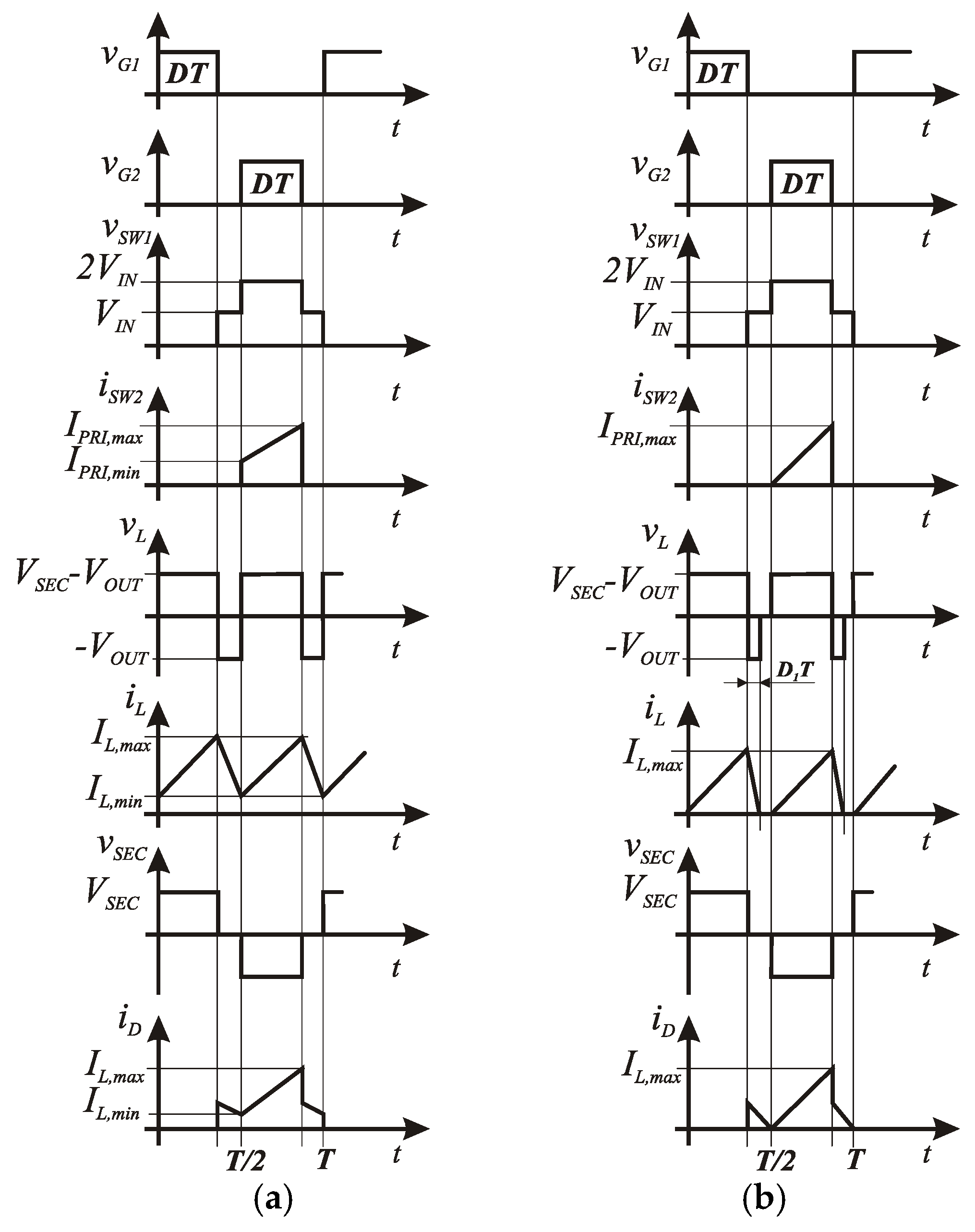
The waveforms of characteristic voltages and currents for the push–pull converter (both operating modes) are illustrated in
Figure 3.
Effective inductor current
IL,eff, in CCM operating mode of the converter, can be derived from the waveform shown in
Figure 3a:
Maximum and minimum values of the inductor current are determined with:
where
IL,avg =
ILOAD. Effective currents through the secondary winding and switch are expressed as:
By knowing the transformer’s turns ratio
n, the maximum (
IPRI,max) and minimum (
IPRI,min) currents are given as follows:
Effective currents through the primary winding and the diode can be determined with:
The average current values through primary winding, secondary winding, and diode, in CCM operating mode, are calculated as:
In DCM operating mode of the converter, the maximum inductor current is
Minimum inductor current and, therefore, the minimum current in the primary winding are equal to zero in this case.
Effective and average current values, when the converter operates in DCM mode, can be derived from the waveforms shown in
Figure 3b. For effective current of the inductor (
IL,eff) we obtain
whereby
D1 is defined as
Effective currents through the switch and the secondary winding are given by
while the effective currents through the primary winding and the diode are calculated as
The average value of the primary current in DCM operating mode is determined with
while (38) and (39) can be used to obtain the average currents through the secondary winding and the diode, respectively.


