Abstract
In this paper, a power regulated circuit (PRC) is proposed for system-on-a-chip (SoC) applications. The proposed PRC is composed of a limiter, a bandgap reference (BGR), three low-dropout regulators (LDOs), and a bias generator. A high output voltage of an active rectifier is given to the limiter, which limits it to a desired supply voltage for circuits in PRC. The curvature-compensated BGR robust to process, voltage and temperature (PVT) variations are designed to provide a stable reference voltage for three LDOs. The three LDOs are implemented to generate regulated output dc voltages. The proposed PRC is designed and fabricated in 130 nm bipolar-CMOS-DMOS (BCD) technology with die area of 1.9 mm × 0.860 mm, including pads. The measurement results show that the limiter limits the input voltage of (6 V to 20 V) to 5.3 V. The BGR produces a stable reference voltage of 1.24 V with a power supply rejection ratio (PSRR) of −58.6 dB and −51.9 dB at 10 Hz and 1 kHz, respectively. The LDO_5V, LDO_3V, and LDO_1.5V generate regulated output dc voltages of 5 V, 3 V, and 1.5 V, respectively, with dc load regulations of 0.43 mV/mA, 0.70 mV/mA, and 0.28 mV/mA while delivering load currents of 300 mA, 100 mA, and 100 mA, respectively.
1. Introduction
During the past decade, wireless power transfer (WPT) has shown unprecedented development and has emerged as one of the promising technologies, especially near field (non-radiative) for wireless charging of electric vehicles, mobile phones, wearable devices, and implanted medical devices to improve user convenience and flexibility [1,2,3,4,5]. Near-field technology is sub-divided into two categories: inductive and capacitive coupling techniques for short-range applications, and magnetic resonance coupling techniques for mid-range applications [6]. Wireless Power Consortium (WPC) and Power Matters Alliance (PMA) standards are based on an inductive coupling technique [7,8], while Alliance for Wireless Power (A4WP) is based on a magnetic resonance coupling technique [9]. The operating frequency for WPC/PMA standards is from 87–357 kHz, while A4WP normally operates at 6.78 MHz. In our work, power is wirelessly transferred from the transmitter to the power receiving unit through A4WP standard. The power receiving unit is composed of an active rectifier, a dc–dc converter, a successive-approximation register (SAR) analog-to-digital converter (ADC), frequency detection, a protection block, a digital block, and a power-up circuit [10]. The active rectifier converts the incoming ac voltage into dc voltage and supplies it to the dc–dc converter and PRC to regulate it for battery and sub-blocks in the power receiving unit. This regulated dc voltage from PRC is also used as the supply voltage for SAR ADC, digital logic block, bias generator, and buffer circuits [11,12]. Since PRC is the subject of this research work, we will concentrate on its suggested architecture and performance.
Due to high increasing demands for wearable/portable devices such as tablet PCs, smartphones, laptops, smart watches, and wireless handsets, the use of power management systems is becoming increasingly important for prolonging the battery life of these devices [13]. A low-dropout (LDO) regulator is an essential block of power management integrated circuits (PMICs) that provide a clean and stable supply voltage to portable devices [14,15]. The high power supply rejection ratio (PSRR), improved line and load regulations, and stability are very demanding specifications for an analog LDO. The PSRR is the measure of how many ripples are rejected or suppressed by the LDO over a wide frequency range, and is expressed as [16,17]:
Recently, a number of techniques have been implemented to improve the abovementioned specifications for the LDO [18,19,20]. These techniques either employ a feed-forward ripple cancelation path or an adaptive path to improve the performance of the LDO. Ref. [21] reports a digital LDO (DLDO) with a feed-forward controller and weight redistribution algorithm (WRA) for line regulation improvement with a transient pump circuit to reduce the undershoot. An event-driven DLDO with an adaptive linear/binary two-step search is presented in [22] to achieve a fast transient response. The adaptive linear search is offered by a two-dimensional circular shift register. A DLDO with a voltage-controlled oscillator (VCO)-based control is described in [23]. The frequencies of the two VCOs in the control loop are controlled by the output voltage and the reference level, respectively. The VCO-based control is a hybrid of analog and digital control schemes. A transient detector is used to improve the transient speed of the DLDO regulator. Similarly, bandgap reference (BGR) generates a reference (fixed) voltage regardless of supply variations, process, temperature changes and circuit loading conditions [24]. The BGR is widely used in many sub-systems such as LDO, a dc–dc converter, SAR ADC, DAC converters, and memories [25]. The bipolar junction transistor (BJT)-based BGR designs are less sensitive to process variations compared to pure-MOSFET designs [26], and can obtain accurate and scalable output [27] among all BGR topologies. There are factors that affect the accuracy of BGR, such as (a) non-linear relation between base-emitter voltage () of BJT and temperature, (b) input offset voltage of operation amplifier for generation of complementary-to-absolute-temperature (CTAT) and proportional-to-absolute-temperature (PTAT) characteristics, and (c) process variations [28]. The of the BJT transistor has a negative temperature co-efficient (TC) (i.e.,) CTAT. The difference between base-emitter voltages of two BJT transistors that have different current densities results in positive TC (i.e.,) PTAT. The of BJT transistor can be written as [29].
where = is the thermal voltage, k is the Boltzmann constant, T is the absolute temperature, and q is the elementary charge of an electron. and are the collector and saturation current, respectively. The CTAT of can be expressed as:
where is the bandgap energy of silicon. Similarly, PTAT due to a difference of of two BJT transistors operating at unequal current densities is shown as:
By solving (3) and (4), we can develop a reference voltage that has nominally zero TC. Mathematically,
where is normally equal to one, and is the ratio of the resistors used in the BGR circuit. Therefore, by choosing the optimum value of the resistors ratio and n, we can generate reference voltage with near-to-zero TC.
In this research work, a power regulated circuit (PRC) for a power receiving unit is presented for system-on-a-chip (SoC) applications. The proposed PRC provides regulated and stable dc voltages for different load conditions, and also serves as supply voltage for sub-blocks such as SAR ADC, digital blocks, bias generator, and buffer circuits in the power receiving unit. The rest of the paper is organized as follows: Section 2 illustrates the block diagram of the proposed PRC. Section 3 discusses the sub-blocks used in the proposed work. Section 4 depicts measurement results. Finally, Section 5 concludes the paper.
2. Proposed Power Regulated Circuit (PRC)
Figure 1 illustrates a block diagram of the proposed PRC used in the power receiving unit. The proposed PRC is composed of a limiter, a BGR circuit, three LDOs, and a bias generator. The active rectifier in the the power receiving unit receives ac voltage of 6.78 MHz frequency and generates a dc voltage (). The limiter in the PRC limits to a desired dc voltage level () and used as a supply voltage for BGR and three LDOs. The supply voltage of the bias generator comes from the output of LDO_3V. The BGR circuit generates a standard reference (fixed) voltage (), regardless of process–voltage–temperature (PVT) variations and circuit load conditions. The standard value lies in the range of 1.2 V to 1.25 V. This is then used in three LDOs and the bias generator circuit. The three LDOs, LDO_5V, LDO_3V, and LDO_1.5V, are designed for different load conditions.
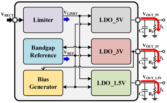
Figure 1.
Block diagram of the proposed power regulated circuit (PRC).
3. Circuit Description
3.1. Limiter Design
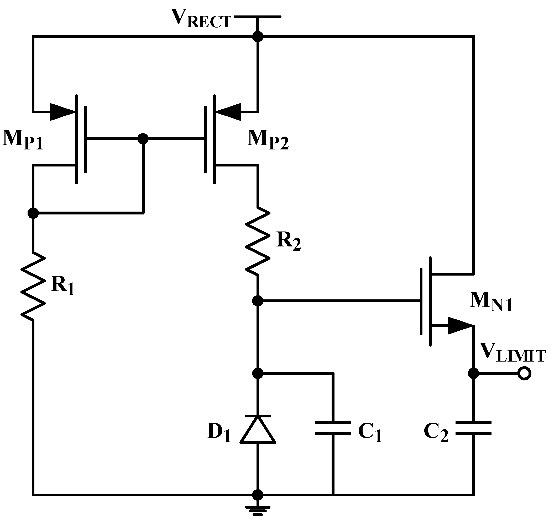
Figure 2 shows the circuit diagram of the limiter used in the proposed PRC. The limiter circuit consists of a zener diode (), high-voltage (24 V) PMOS ( and ), and a NMOS transistor (). A high-output dc voltage of an active rectifier is fed to the limiter circuit, which limits it to a desired dc voltage level for supply of other circuits such as BGR, three LDOs, and bias generator in the PRC. A bias voltage is given to the gates of and to turn them on and allows the current to flow in the circuit. An optimum gate voltage for is a developed courtesy resistor (), zener diode (), and a capacitor () to generate desired dc voltage () at the output, as shown in Figure 2. This limiter circuit can draw a current of 520 A to support other blocks in the PRC.

Figure 2.
Circuit diagram of the proposed limiter in the PRC.
3.2. Bandgap Reference (BGR) Design
Figure 3 presents a circuit diagram of the BGR implemented in the PRC. A two-stage op-amp is used in the BGR. The op-amp adjusts the gate voltage of the PMOS transistors in order to equalize terminal voltages and . In addition, the op-amp provides sufficient loop gain and an acceptable phase margin and bandwidth. The start-up circuit and op-amp provide a fast settling time to the BGR. The output voltage of the BGR exhibits a nominally zero TC. Performing Kirchhoff’s voltage law (KVL) at results in:
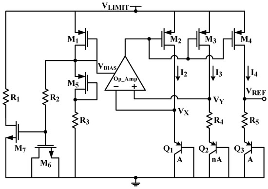
Figure 3.
Circuit diagram of the proposed bandgap reference (BGR) in the PRC.
Similarly, applying KVL at results in:
Since op-amp equalizes and , it can be written as:
By putting (4) in (8), is given by:
Since, = , the of the BGR can be written as:
Thus, with near-to-zero TC can be generated by finding the optimum values of n, and .
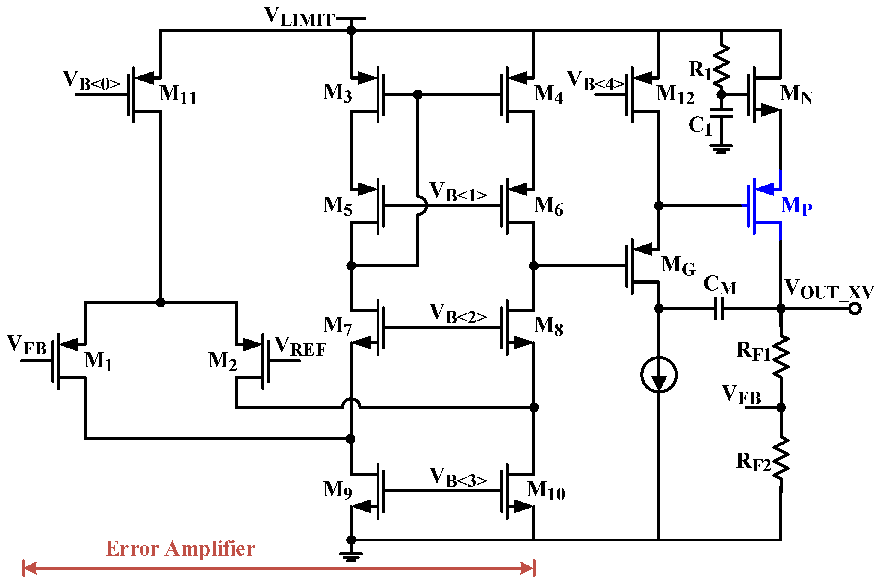
3.3. Low-Dropout Regulator (LDO) Design
Figure 4 depicts a circuit diagram of the proposed LDO used in the PRC. The circuit structure for all three LDOs is the same. However, the sizes of the transistors, bias voltages, capacitors, resistors, and the PMOS pass transistor () are different for three LDOs. For instance, the width of for LDO_5V, LDO_3V, and LDO_1.5V is 8 mm, 1.2 mm, and 0.8 mm, respectively, while the channel length is set to the minimum. A high open-loop gain error amplifier (EA) is used to provide an acceptable PSRR at the gate of the transistor . The acts as a common gate transistor between and the output of the EA. The capacitor provides stability to LDO by applying Miller’s theorem. An NMOS transistor is cascaded with to improve the PSRR of the LDO. The shields the from power supply variations. The gate of is biased using a simple RC filter, which further minimizes ripples at gate of the . The open-loop gain () of is given by:
where and are the transconductance and output resistance of , respectively. The feedback voltage () can be written as:
where A is the open-loop gain of EA. The closed–closed transfer function of the LDO is given by:

Figure 4.
Circuit diagram of the proposed low-dropout regulator (LDO) in the PRC.
If loop gain () is much higher than one, then PSRR can be related to the open loop gain as:
Thus, open-loop gain and feedback resistors ( and ) play a critical role in the performance of the LDO.
4. Measurement Results
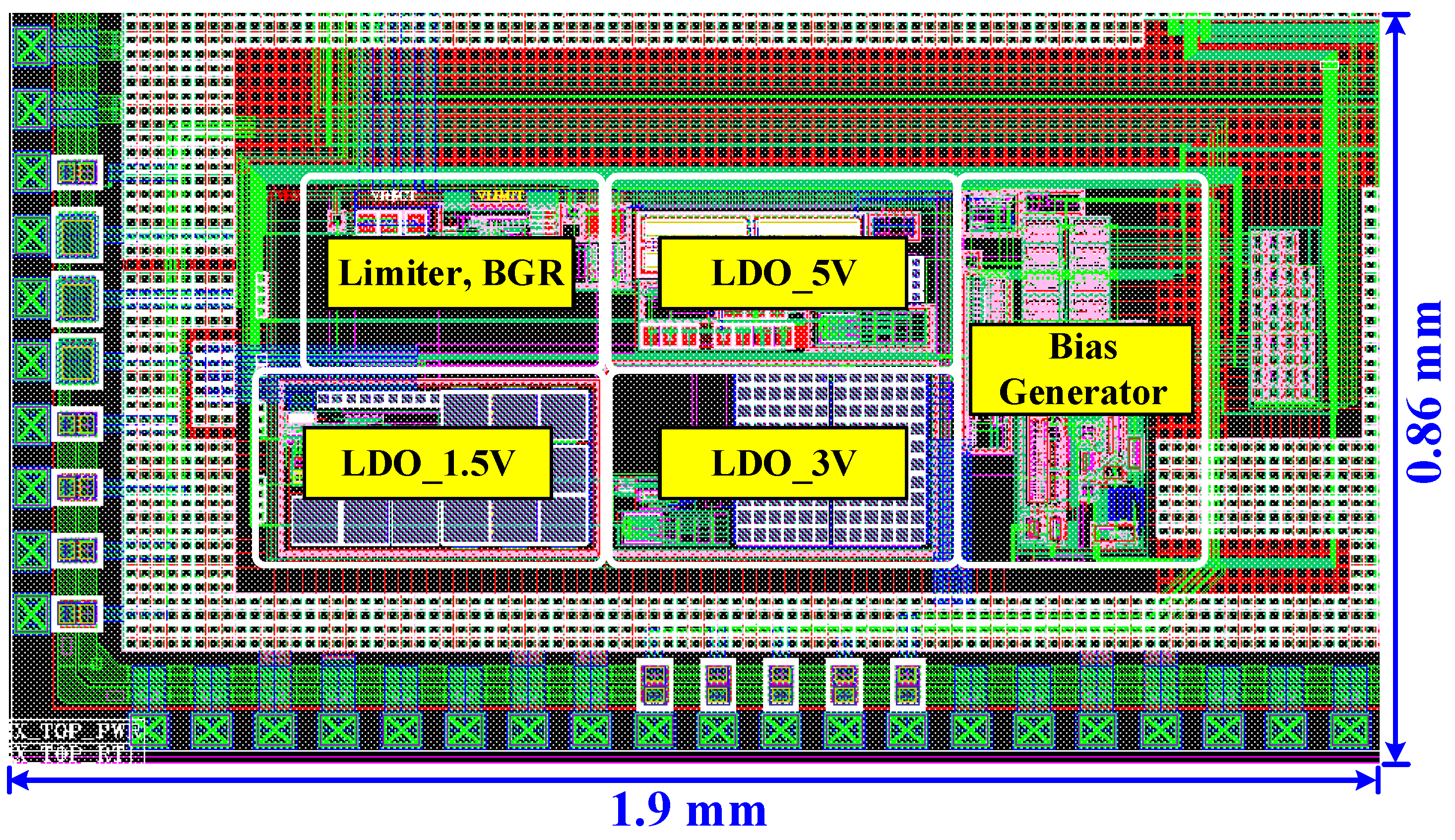
Figure 5 shows the top layout pattern of the proposed PRC with a layout area of 1.9 mm × 0.860 mm, including pads. The circuit is designed and fabricated in a 130 nm BCD process.
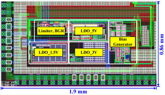
Figure 5.
Top layout pattern of the proposed power regulated circuit (PRC).
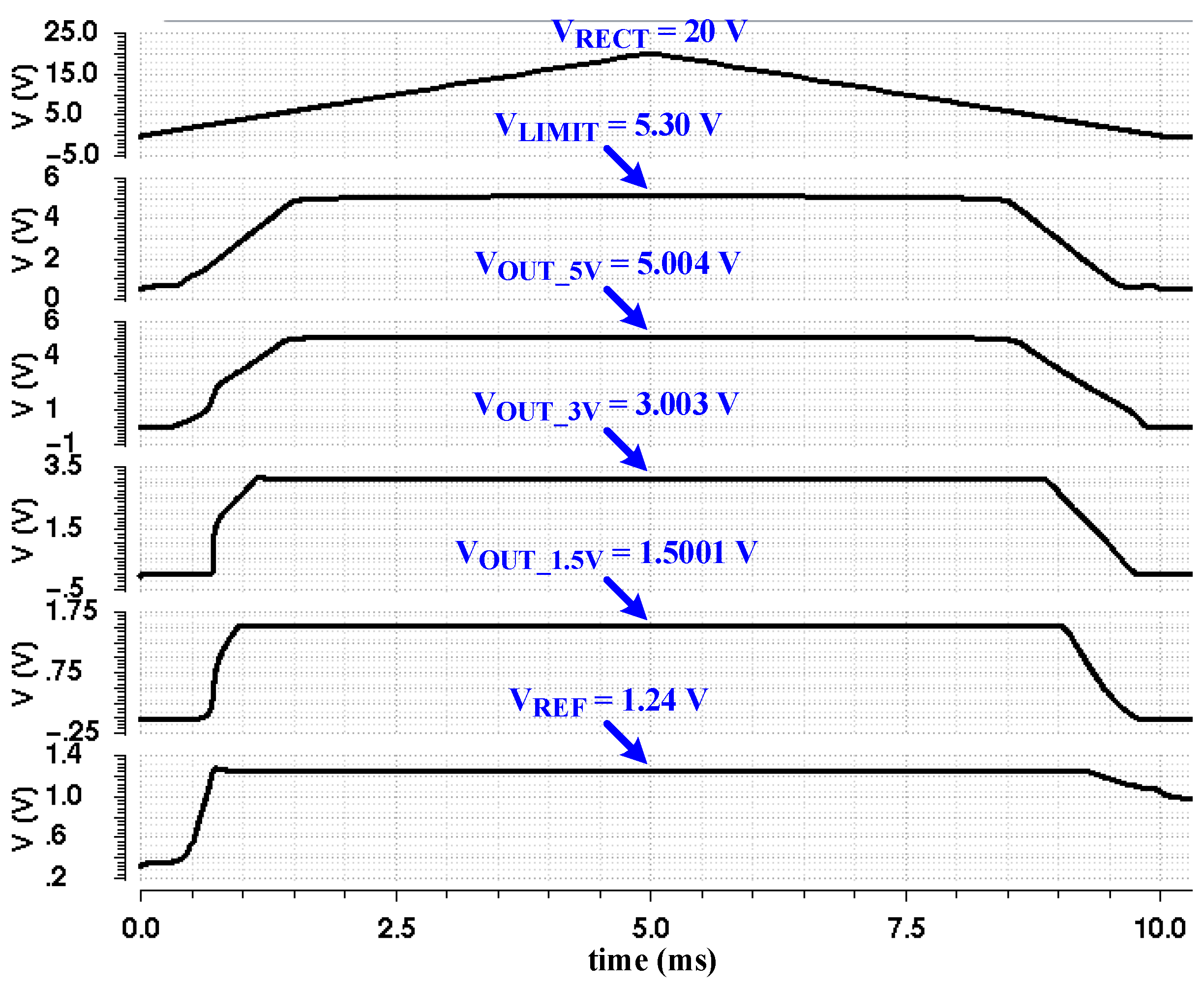
Figure 6 demonstrates post layout simulation results of PRC. The supply voltage ( in this case) is swept from 0 to 20 V and back to 0 to check the performance of PRC. It can be seen that PRC operates normally in this supply range. The limiter produces a desired output voltage () of 5.3 V for this wide range of . This is used as a supply voltage for other circuits in the PRC. The BGR provides a stable reference voltage () of 1.24 V. The BGR requires minimum of 2 V. From 2 to 5.5 V, the BGR produces stable of 1.24 V. The LDO_5V, LDO_3V, and LDO_1.5V generate regulated output dc voltages (, , and ) of 5.004 V, 3.003 V, and 1.5001 V, respectively. The total current consumption of PRC is 176.4 A.
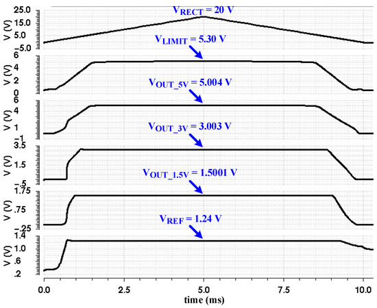
Figure 6.
Top simulation results of the proposed power regulated circuit (PRC).
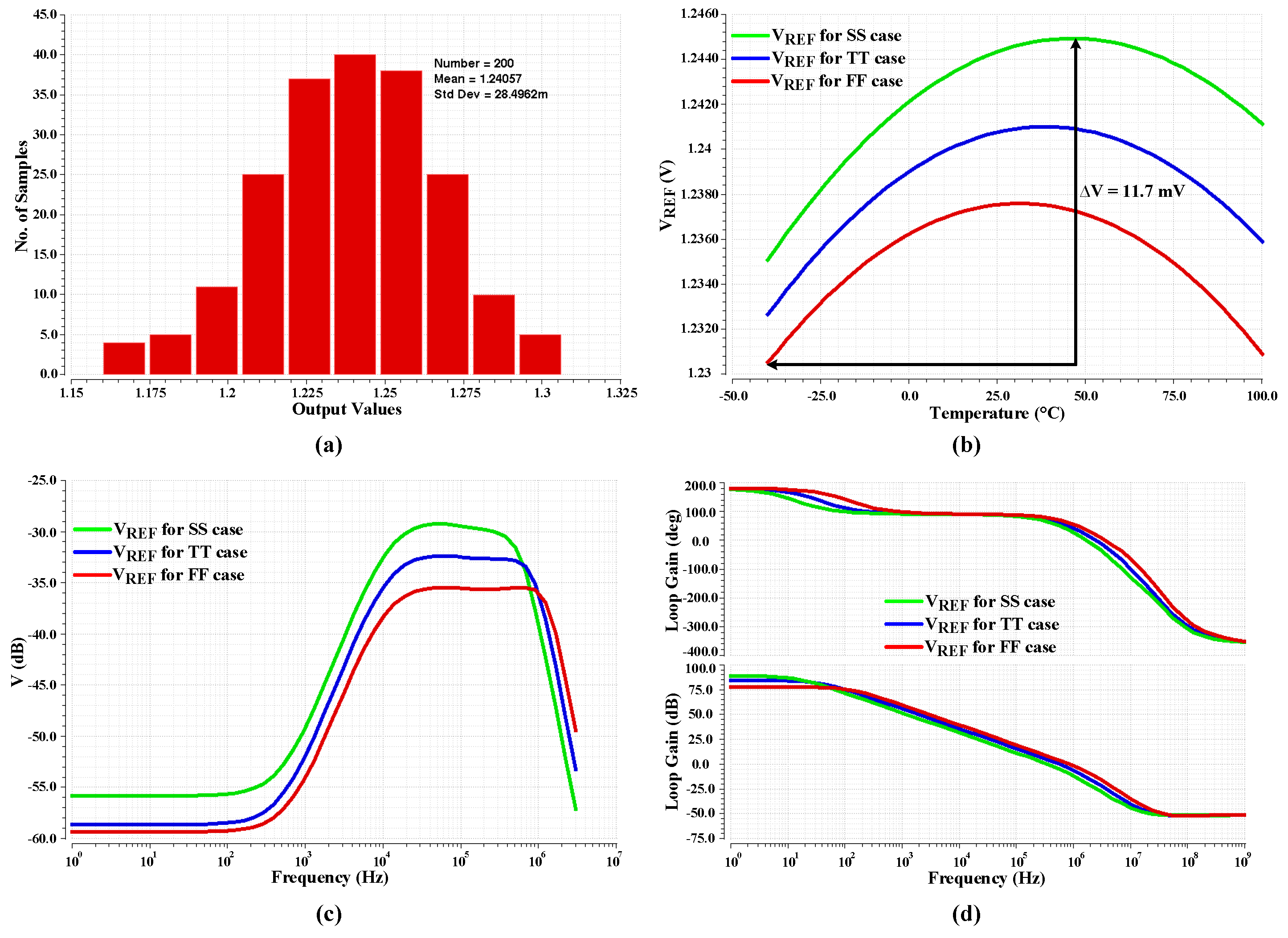
Figure 7 displays post-simulation results of the BGR. Figure 7a shows the result of 200 Monte Carlo runs for the BGR. The mean value of the BGR for 200 runs is 1.24 V, with standard deviation of 28.49 mV. Here, all the mismatch (including CMOS transistors, resistors, and BJT transistors) and process variations in the BGR circuit are considered. The mismatch shows a shift (left or right) in the output voltage () caused by the non-idealities. Figure 7b presents for different corner cases (SS, TT, and FF) over a temperature range from −40 °C to 100 °C. The maximum deviation (V) in for this temperature range is 11.7 mV, which is acceptable and satisfies TC of the BGR. The mean value of at 30 °C is 1.24 V. Figure 7c depicts PSRR of the BGR for different corner cases. The values of PSRR at 10 Hz frequency for SS (4.5 V, 100 °C), TT (5 V, 30 °C), and FF (5.5 V, −40 °C) are −55.7 dB, −58.6 dB, and −59.3 dB, respectively. Similarly, values of PSRR at 1 kHz for SS, TT, and FF are −49.1 dB, −51.9 dB, and −54.1 dB, respectively. This demonstrates good PSRR over a wide frequency range. Figure 7d shows a stability check of the BGR for different corner cases. The loop gain and phase margin of BGR for SS, TT, and FF conditions are (87.2 dB, 64.5°), (83.5 dB, 63.2°), and (77.1 dB, 60.5°), respectively. These results show that the proposed BGR operates well regardless of the PVT variations.

Figure 7.
Post-simulation results of the proposed BGR. (a) Monte Carlo simulation. (b) Output voltage’s variation over temperature range. (c) PSRR for different corner cases. (d) Stability check.
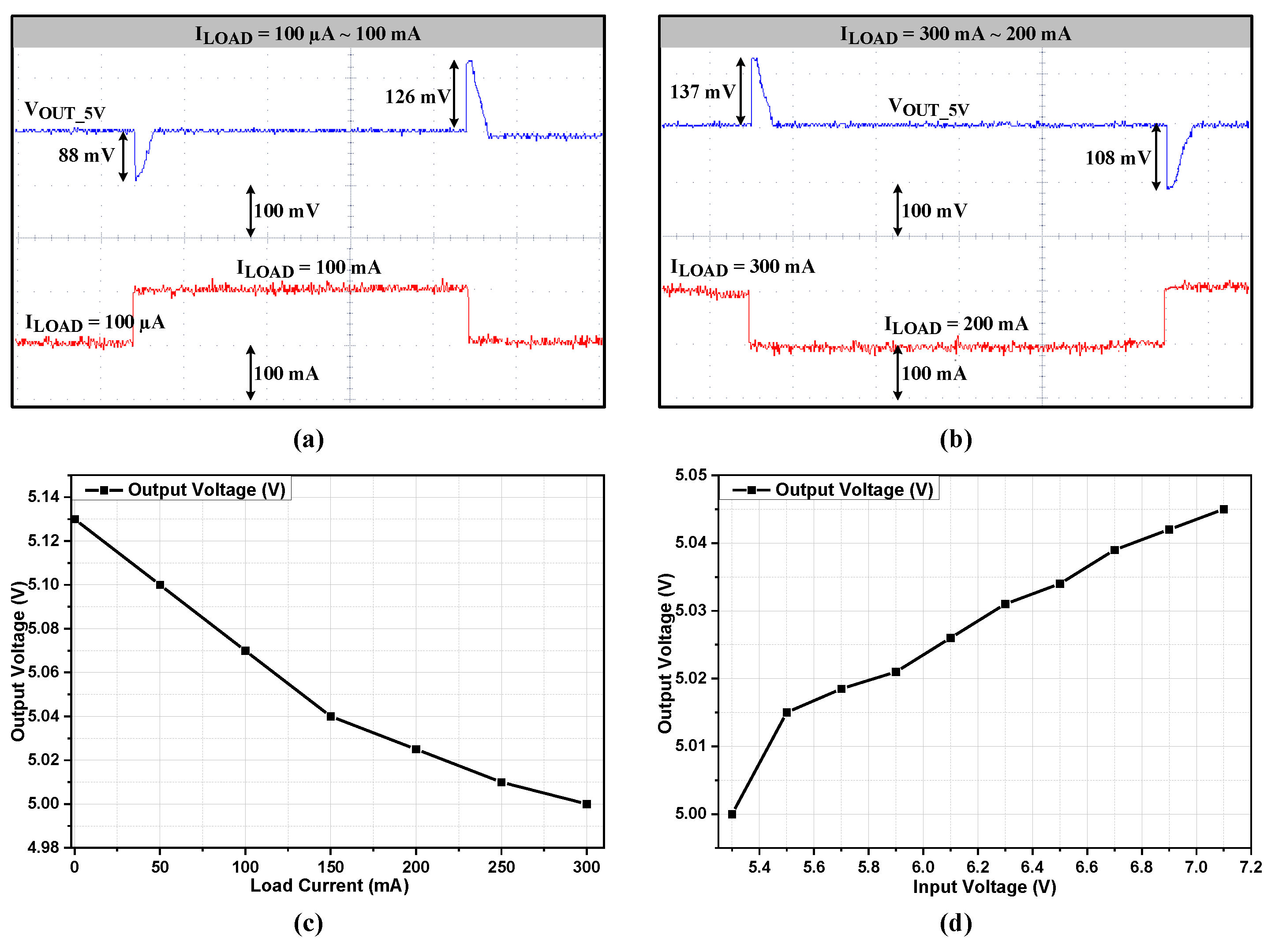
Figure 8 demonstrates measured results of LDO_5V. Figure 8a shows load transient response from 100 A to 100 mA. The LDO_5V displays a stable settling behavior with a 1 F output ceramic capacitor. The maximum undershoot and overshoot are 88 mV and 126 mV, respectively, with a 100 mA step load current. Similarly, Figure 8b presents a load transient response from 300 mA to 200 mA, with maximum overshoot and undershoot of 137 mV and 108 mV, respectively. Figure 8c depicts load regulation for a wide range of load current, 10 A to 300 mA. The dc fluctuation in the output voltage is nearly 130 mV over the wide load current range, which is 2.6% of the output voltage ( = 5 V). Figure 8d shows line regulation for input voltage range of 5.3 V to 7.1 V at 300 mA load current. The dc variation in the output voltage is 45 mV, which shows good line regulation.
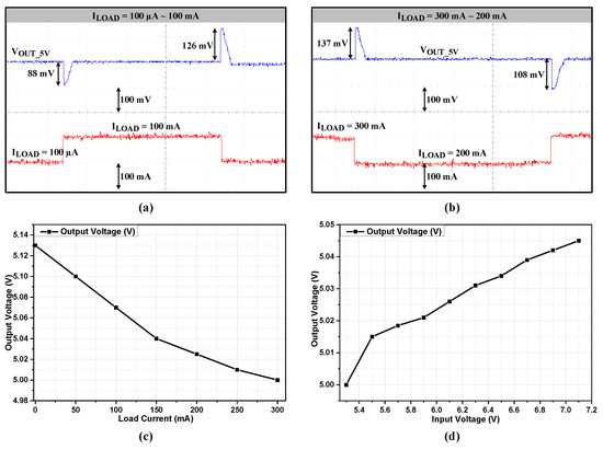
Figure 8.
Measured results of LDO_5V. (a) Load transient response from 100 A to 100 mA. (b) Load transient response from 300 mA to 200 mA. (c) Load regulation. (d) Line regulation.
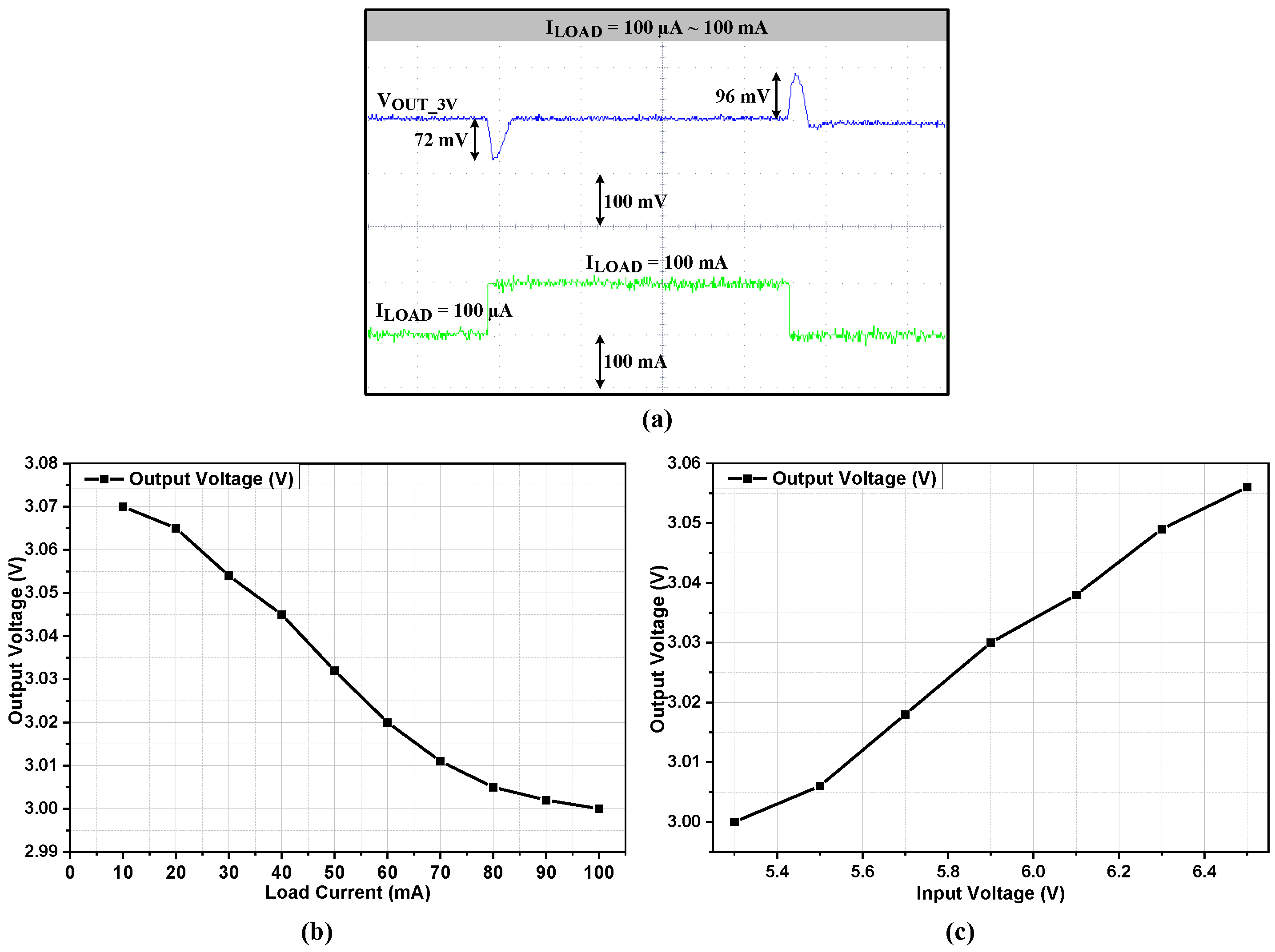
Figure 9 shows measurement results of LDO_3V. Figure 9a depicts a load transient response from 100 A to 100 mA with maximum undershoot and overshoot of 72 mV and 96 mV, respectively. Figure 9b displays load regulation for a load current ranging from 10 A to 100 mA. The dc variation in the output voltage is around 70 mV, which is 2.34% of the output voltage ( = 3V). Figure 9c presents line regulation at 100 mA load current for input range of 5.3 V to 6.5 V. The dc variation in output voltage for this input voltage range is 56 mV.
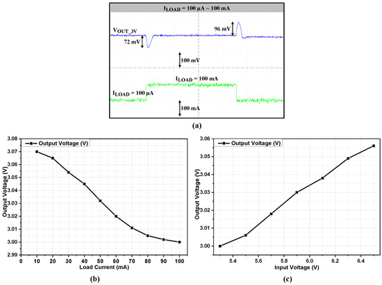
Figure 9.
Measured results of LDO_3V. (a) Load transient response from 100 A to 100 mA. (b) Load regulation. (c) Line regulation.
Figure 10 presents measured results of LDO_1.5V. Figure 10a shows load transient response from 100 A to 100 mA with maximum undershoot and overshoot of 62 mV and 84 mV, respectively. Like LDO_3V, LDO_1.5V is designed for the same load current condition of 10 A to 100 mA. Figure 10b depicts load regulation with dc variation in output voltage of around 28 mV, which is 1.86% of the output voltage ( = 1.5 V). Figure 10c displays line regulation at 100 mA load with dc variation in the output voltage of around 71 mV.
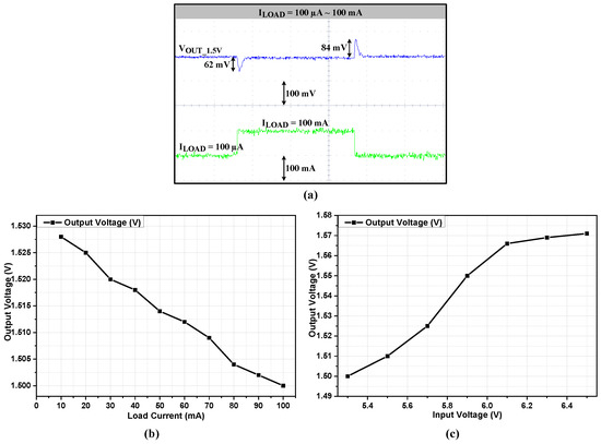
Figure 10.
Measured results of LDO_1.5V. (a) Load transient response from 100 A to 100 mA. (b) Load regulation. (c) Line regulation.
Since most of the research works have been carried out on either BGR or LDO, Table 1 compares the proposed LDOs with recently published works. The proposed LDOs show better performance than the reported works in terms of a wide range of load current, quiescent current, line and load regulations. However, the proposed PRC has a larger die area.

Table 1.
Performance summary.
5. Conclusions
This paper presents a PRC for a power receiving unit for system-on-a-chip (SoC) applications. The proposed PRC is comprised of a limiter, a BGR, three LDOs, and a bias generator. The PRC works in such a way that the limiter limits the high output voltage of an active rectifier to the desired voltage for the power supply of BGR, three LDOs, and a bias generator. The BGR produces a stable (fixed) reference voltage for LDOs, regardless of the PVT variations. The three LDOs are designed to generate regulated output dc voltages with improved PSRR, and line and load regulation performances. The proposed PRC is designed and implemented in 130 nm BCD technology. The measurement results reveal that the limiter limits the output voltage (6 V to 20 V) of the active rectifier to 5.3 V. The BGR provides a reference voltage of 1.24 V with PSRR of −58.6 dB and −51.9 dB at 10 Hz and 1 kHz, respectively. The LDO_5V, LDO_3V, and LDO_1.5V generate regulated output dc voltages of 5 V, 3 V, and 1.5 V, respectively. These LDOs are capable of delivering 300 mA, 100 mA, and 100 mA load currents with dc load regulations of 0.43 mV/mA, 0.70 mV/mA, and 0.28 mV/mA, respectively.
Author Contributions
Conceptualization, D.K.; methodology, D.K.; software, D.K.; validation, D.K., M.B. and Q.u.A.; formal analysis, D.K., S.A.A.S. and K.S.; investigation, D.K., M.B., K.S. and D.V.; resources, D.K., K.S. and K.-Y.L.; data curation, D.K. and M.B.; writing—original draft preparation, D.K.; writing—review and editing, D.K. and K-Y.L.; visualization, D.K., S.A.A.S. and Q.A.; supervision, K.-Y.L.; project administration, K.-Y.L.; funding acquisition, K.-Y.L. All authors have read and agreed to the published version of the manuscript.
Funding
This paper was supported by Korea Institute for Advancement of Technology (KIAT) grant funded by the Korea Government(MOTIE) (P0012451, The Competency Development Program for Industry Specialist).
Institutional Review Board Statement
Not applicable.
Informed Consent Statement
Not applicable.
Data Availability Statement
Data sharing is not applicable to this article.
Conflicts of Interest
The authors declare no conflict of interest.
References
- Hekal, S.; Abdel-Rahman, A.B.; Jia, H.; Allam, A.; Barakat, A.; Pokharel, R.K. A Novel Technique for Compact Size Wireless Power Transfer Applications Using Defected Ground Structures. IEEE Trans. Microw. Theory Technol. 2017, 65, 591–599. [Google Scholar] [CrossRef]
- Jonah, O.; Georgakopoulos, S.V. Wireless Power Transfer in Concrete via Strongly Coupled Magnetic Resonance. IEEE Trans. Antennas Propag. 2013, 61, 1378–1384. [Google Scholar] [CrossRef]
- Yalong, Z.; Xueliang, H.; Jiaming, Z.; Linlin, T. Design of wireless power supply system for the portable mobile device. In Proceedings of the 2013 IEEE International Wireless Symposium (IWS), Beijing, China, 14–18 April 2013; pp. 1–4. [Google Scholar]
- Huh, J.; Lee, S.W.; Lee, W.Y.; Cho, G.H.; Rim, C.T. Narrow-Width Inductive Power Transfer System for Online Electrical Vehicles. IEEE Trans. Power Electron. 2011, 26, 3666–3679. [Google Scholar] [CrossRef]
- Wang, G.; Liu, W.; Sivaprakasam, M.; Kendir, G.A. Design and analysis of an adaptive transcutaneous power telemetry for biomedical implants. IEEE Trans. Circuits Syst. I Reg. Papers. 2005, 52, 2109–2117. [Google Scholar] [CrossRef]
- Kalwar, K.; Aamir, M.; Mekhilef, S. Inductively coupled power transfer (ICPT) for electric vehicle charging—A review. Renew. Sustain. Energy Rev. 2015, 47, 62–475. [Google Scholar] [CrossRef]
- Wireless Power Consortium. System Description, Wireless Power Transfer—Vol. I: Low Power, Part 1: Interface Definition, Version 1.0; Wireless Power Consortium: Piscataway, NJ, USA, 2010. [Google Scholar]
- Texas Instrument. Introduction to Wireless Power; Texas Instrument: Dallas, TX, USA, 2012; pp. 1–49. [Google Scholar]
- Tseng, R.; von Novak, B.; Shevde, S.; Grajski, K.A. Introduction to the alliance for wireless power loosely-coupled wireless power transfer system specification version 1.0. In Proceedings of the 2013 IEEE Wireless Power Transfer (WPT), Perugia, Italy, 15–16 May 2013; pp. 79–83. [Google Scholar]
- Park, H.G.; Jang, J.H.; Kim, H.J.; Park, Y.J.; Oh, S.; Pu, Y.; Lee, K.Y. A Design of a Wireless Power Receiving Unit With a High-Efficiency 6.78-MHz Active Rectifier Using Shared DLLs for Magnetic-Resonant A4WP Applications. IEEE Trans. Power Electron. 2016, 31, 4484–4498. [Google Scholar] [CrossRef]
- Oh, S.J.; Khan, D.; Jang, B.G.; Basim, M.; Asif, M.; Ali, I.; Lee, K.Y. A 15-W Quadruple-Mode Reconfigurable Bidirectional Wireless Power Transceiver With 95% System Efficiency for Wireless Charging Applications. IEEE Trans. Power Electron. 2021, 36, 3814–3827. [Google Scholar] [CrossRef]
- Park, Y.J.; Jang, B.; Park, S.M.; Ryu, H.C.; Oh, S.J.; Kim, S.Y.; Lee, K.Y. A Triple-Mode Wireless Power-Receiving Unit With 85.5% System Efficiency for A4WP, WPC, and PMA Applications. IEEE Trans. Power Electron. 2018, 33, 3141–3156. [Google Scholar] [CrossRef]
- Park, C.; Onabajo, M.; Silva-Martinez, J. External Capacitor-Less Low Drop-Out Regulator With 25 dB Superior Power Supply Rejection in the 0.4–4 MHz Range. IEEE J. Solid-State Circuits 2014, 49, 486–501. [Google Scholar] [CrossRef]
- Keikhosravy, K.; Mirabbasi, S. A 0.13-µm CMOS Low-Power Capacitor-Less LDO Regulator Using Bulk-Modulation Technique. IEEE Trans. Circuits Syst I Reg. Papers 2014, 61, 3105–3114. [Google Scholar] [CrossRef]
- Maity, A.; Patra, A. A Single-Stage Low-Dropout Regulator with a Wide Dynamic Range for Generic Applications. IEEE Trans. Very Large Scale Integr. (VLSI) Syst. 2016, 24, 2117–2127. [Google Scholar] [CrossRef]
- Khan, D.; Abbasizadeh, H.; Khan, Z.H.N.; Park, Y.; Lee, K. Design of a capacitor-less LDO with high PSRR for RF energy harvesting applications. In Proceedings of the 2017 International SoC Design Conference (ISOCC), Seoul, Korea, 5–8 November 2017; pp. 202–203. [Google Scholar]
- Asif, M.; Ali, I.; Khan, D.; Rehman, M.R.U.; Basim, M.; Pu, Y.G.; Lee, K.Y. A High Performance Adaptive Digital LDO Regulator with Dithering and Dynamic Frequency Scaling for IoT Applications. IEEE Access 2020, 8, 32200–132211. [Google Scholar] [CrossRef]
- El-Nozahi, M.; Amer, A.; Torres, J.; Entesari, K.; Sanchez-Sinencio, E. High PSR Low Drop-Out Regulator With Feed-Forward Ripple Cancellation Technique. IEEE J. Solid-State Circuits 2010, 45, 565–577. [Google Scholar] [CrossRef]
- Yang, B.; Drost, B.; Rao, S.; Hanumolu, P.K. A high-PSR LDO using a feedforward supply-noise cancellation technique. In Proceedings of the 2011 IEEE Custom Integrated Circuits Conference (CICC), San Jose, CA, USA, 19–21 September 2011; pp. 1–4. [Google Scholar]
- Heng, S.; Pham, C. A Low-Power High-PSRR Low-Dropout Regulator with Bulk-Gate Controlled Circuit. IEEE Trans. Circuits Syst. II Exp. Briefs 2010, 57, 245–249. [Google Scholar] [CrossRef]
- Chen, B.H.; Wu, T.Y.; Zheng, K.L.; Chen, K.H.; Lin, Y.H.; Lin, S.R.; Tsai, T.Y. A Feedforward Controlled Digital Low-Dropout Regulator With Weight Redistribution Algorithm and Body Voltage Control for Improving Line Regulation With 99.99% Current Efficiency and 0.5-mV Output Voltage Ripple. IEEE J. Solid-State Circuits 2022, 1–11. [Google Scholar] [CrossRef]
- Song, Y.; Oh, J.; Cho, S.-Y.; Jeong, D.-K.; Park, J.-E. A Fast Droop-Recovery Event-Driven Digital LDO With Adaptive Linear/Binary Two-Step Search for Voltage Regulation in Advanced Memory. IEEE Trans. Power Electron. 2022, 37, 1189–1194. [Google Scholar] [CrossRef]
- Kang, J.-G.; Park, J.; Jeong, M.-G.; Yoo, C. Digital Low-Dropout Regulator with Voltage-Controlled Oscillator Based Control. IEEE Trans. Power Electron. 2022, 37, 6951–6961. [Google Scholar] [CrossRef]
- Krolak, D.; Plojhar, J.; Horsky, P. An Automotive Low-Power EMC Robust Brokaw Bandgap Voltage Reference. IEEE Trans. Electromagn. Comp. 2020, 62, 2277–2284. [Google Scholar] [CrossRef]
- Yu, C.; Siek, L. An Area-Efficient Current-Mode Bandgap Reference with Intrinsic Robust Start-Up Behavior. IEEE Trans. Circuits Syst. II Exp. Briefs 2015, 62, 937–941. [Google Scholar] [CrossRef]
- De Vita, G.; Iannaccone, G. A Sub-1-V, 10 ppm/ C, Nano power Voltage Reference Generator. IEEE J. Solid-State Circuits 2007, 42, 1536–1542. [Google Scholar] [CrossRef]
- Sanborn, K.; Ma, D.; Ivanov, V. A sub-1-V low noise bandgap voltage reference. IEEE J. Solid-State Circuits 2007, 42, 2466–2481. [Google Scholar] [CrossRef]
- Chen, K.; Petruzzi, L.; Hulfachor, R.; Onabajo, M. A 1.16-V 5.8-to-13.5-ppm/°C Curvature-Compensated CMOS Bandgap Reference Circuit With a Shared Offset-Cancellation Method for Internal Amplifiers. IEEE J. Solid-State Circuits 2021, 56, 267–276. [Google Scholar] [CrossRef]
- Rezavi, B. Design of Analog CMOS Integrated Circuits, 2nd ed.; McGraw Hill: New York, NY, USA, 2015. [Google Scholar]


Publisher’s Note: MDPI stays neutral with regard to jurisdictional claims in published maps and institutional affiliations. |
© 2022 by the authors. Licensee MDPI, Basel, Switzerland. This article is an open access article distributed under the terms and conditions of the Creative Commons Attribution (CC BY) license (https://creativecommons.org/licenses/by/4.0/).