Article

A 5 V-to-32 V Input PVT-Robust Charge-Pump Circuit with Adjustable Output in a 0.18 μm BCD Process

1
Institute of Microelectronics of the Chinese Academy of Sciences, Beijing 100029, China
2
University of Chinese Academy of Sciences, Beijing 100049, China
3
Hangzhou Zhongke Microelectronics Co., Ltd., Hangzhou 310053, China
*
Author to whom correspondence should be addressed.
Electronics 2022, 11(18), 2828; https://doi.org/10.3390/electronics11182828
Submission received: 30 July 2022 / Revised: 1 September 2022 / Accepted: 2 September 2022 / Published: 7 September 2022

Abstract

:
In this paper, a new closed-loop charge-pump circuit with adjustable output voltage and an on-chip compensation technique is proposed. The environmental temperature and process corner can be detected with an on-chip detection circuit and automatically feedback an adjusted reference voltage. With this, the magnitude of the charge-pump output voltage with Pulse-Width Modulation (PWM) can be compensated. The charge-pump circuit is designed and verified with a 180 nm Bipolar-CMOS-DMOS (BCD) process, and its output voltage at different process, voltage, and temperature (PVT) is controllable with low ripple. There are three selections for adjusting the output voltage: +5 V/+7 V/+10 V shifts, with the supply voltage ranging from 5 V to 32 V. It can remain tunable and stable at any shifts. The maximum deviation is ±0.265%, and the maximum load current can reach 30 mA. The ripple voltage is less than 0.3% ( Δ Vripple/Vout) underthe maximum load. The Monte Carlo simulation results show that the worst case of the process sensitivity ( σ / μ ) is 0.1%. The charge-pump core area is 0.308 mm 2 , and the power consumption is 4.753 mW. The circuit can produce high-precision output and is suitable for high-side driving IC applications.

1. Introduction

The charge pump is a critical part of portable electronic equipment for its small size and easy integration. In addition, it is one of the most widely applied power converters, especially for boosting the supply voltage. For example, charge-pump circuits are widely applied in liquid-crystal display (LCD) systems and in driving analog switching systems where a voltage higher than the supply voltage is required. The required power supply voltage is usually a different attribute to its broad application scenarios. Therefore, the charge pump with fixed voltage cannot meet the different power supply requirements, which requires a voltage-adjust charge pump to provide a variety of output voltages or currents [1].
PVT variation has attracted more and more attention owing to the shrinking size of the manufacturing process. The chip performance from a different location can be quite different due to the continuous increase in the process deviation caused by manufacturing process fluctuation. The output voltage is quite sensitive to the PVT variations for a conventional open-loop charge-pump circuit. To stabilize the output voltage, the feedback mechanism is applied to regulate the output. Common feedback mechanisms include Pulse-Width Modulation (PWM) [2,3], Pulse-Skip Modulation (PSM) [4], Variable Frequency Modulation (VFM) [5,6], input current-limiting control [7], etc. It is usually necessary to ensure that the desired indicators are achieved in the worst case during the circuit design. However, the output voltage will be higher than the set voltage under other conditions. Therefore, robust technology becomes increasingly necessary to enhance the circuit performance and avoid functional faults [8].
Various methods in different fields are used to reduce the performance loss caused by PVT variations [9]. For the whole-system PVT robust, its output transfer function can be designed to consist of the capacitance ratio and the transistor size ratio. The voltage gain is expected to remain constant, given that both the capacitance ratio and the transistor size ratio are independent of the PVT variations [10], under the condition of heavy hardware consumption. The amplifier’s gain can be compensated by tracking the PVT variations by an auxiliary single-pole amplifier [11]. Alternatively, the circuit’s operating environment can be directly detected by PVT detector to regulate the circuit [12,13,14,15]. In this design, adjusting the amplifier’s reference voltage under various PVT situations can precisely control the output voltage by the regulation system. Consequently, a circuit for on-chip process corner detection is required to achieve it. Currently, there are various techniques for process corner detection, one of which is generating a voltage signal unrelated to temperature and only relevant to process corners and transmitting it to a TDC (Time-to-Digital Converter) to distinguish the process corners. However, it is challenging to maintain the clock delay of the D flip-flop constant in AD converters, and only a few temperature nodes may be distinguished. In addition, the current process corner can be judged according to the fluctuation of the VTH, while temperature variations can also impact the VTH. It is likely to generate overlapping phenomena and make it impossible to identify the process corners if the temperature detection range is too large [12].
The adjustable output voltage is preferred to satisfy more applications. Typically, the adjustable output voltage can be accomplished by altering the voltage conversion rate (VCR) of the charge pump [16,17,18,19]. However, the conversion efficiency will be reduced due to the influence of the parasitic capacitance by changing the series or parallel connection between the floating capacitors to change the VCR. It can be improved by folding floating capacitors into other floating capacitors or coupling capacitors to alter the charge pump’s actual order between the input and output. However, it is still the cost of a large chip area.
This paper proposes a new closed-loop charge pump with adjustable output voltage and PVT robust. In order to reduce the effect of the PVT on the output voltage VCP, we propose a new process corner detection circuit that can detect in a wide temperature range. At the same time, according to the demand for an external load power supply, the output voltage VCP can be adjusted to provide a range of10–42 V. There are three selections for adjusting the output voltage: +5 V/+7 V/+10 V shifts, with supply voltage ranging from 5 V to 32 V. It can remain tunable and stable at any shifts. Thus, the application is wide. The PWM modulation combines the characteristics of the PVT robust and the adjustable output voltage to save area and power consumption. The proposed charge-pump circuit’s system design is described in Section 2. The implementation of critical circuits is covered in Section 3. The simulation results are shown in Section 4. The paper is summarized in Section 5.

2. System Design

The proposed charge-pump circuit consists of a switched capacitor module, a PWM modulation module, a high-voltage LDO module, and an output voltage modulation module, as shown in Figure 1. The high-voltage LDO module, in which VBB is the input power supply voltage (5–32 V), converted to a low-voltage VDD (5 V), provides the power supply voltage for the low-voltage module in the chip.
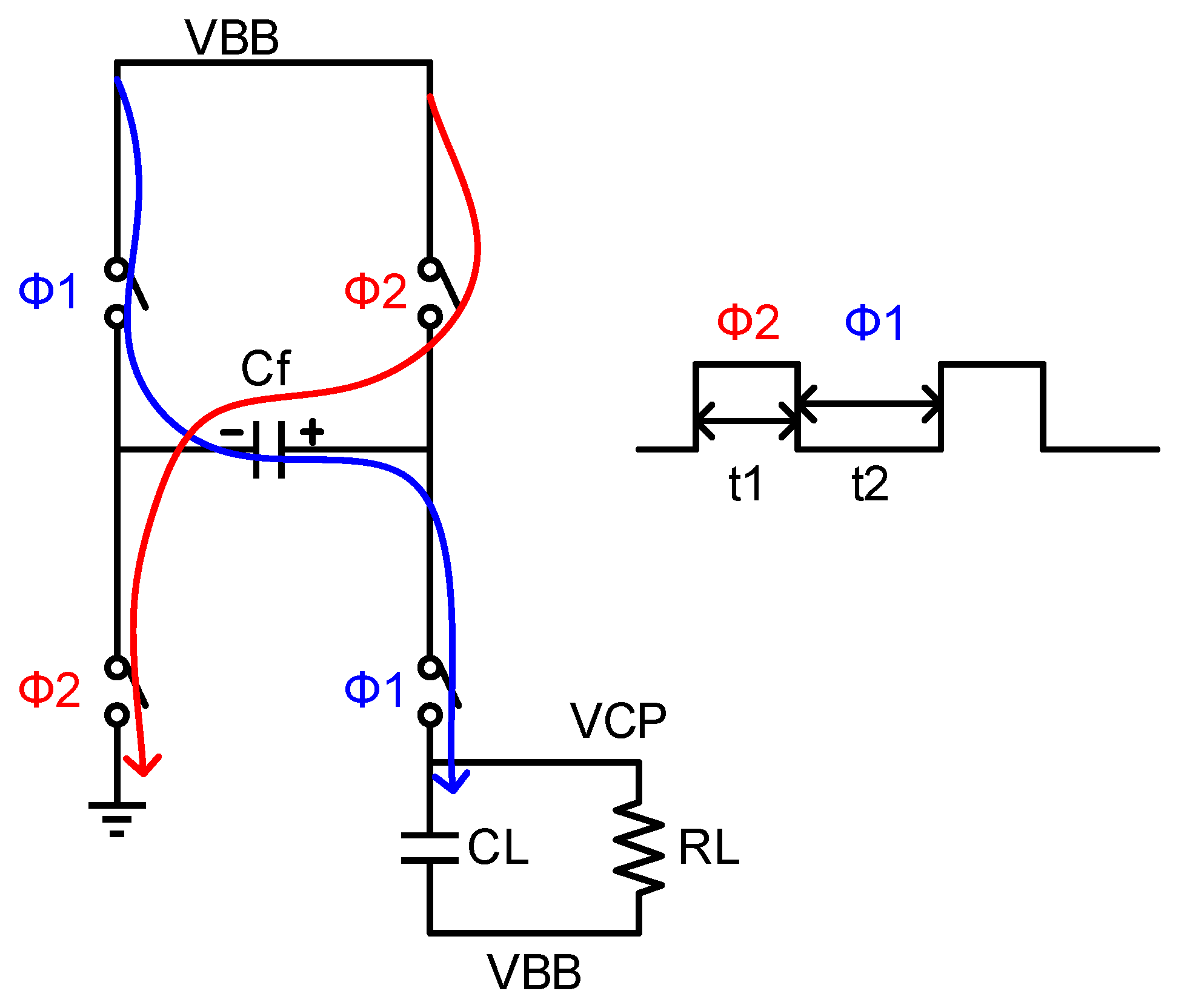
The switched capacitor module operates on the following principles. Firstly, the switched transistors MN1 and MN2 are turned on, and the switched transistors MP1 and MP2 are turned off. The pump capacitor Cf is charged by VBB so that the positive plate potential of the pump capacitor is VBB, and the negative plate potential is 0. In the next cycle, the switched transistors MN1 and MN2 are turned off, the switched transistors MP1 and MP2 are turned on, and the negative plate potential of the pump capacitor is VBB. Because the voltage on the capacitor cannot vary abruptly, the potential of the positive plate is VBB+ Δ V using the characteristic that the voltage on the capacitor cannot be mutated. The charge on the capacitor is transferred to the load capacitor to obtain the output boost signal VCP. During this process, the Vpulse signal controls the switches through different drive circuits, so that the switches on the same branch are not simultaneously turned on.
A schematic diagram of the switching capacitance module is shown in Figure 2. The power supply voltage VBB charges Cf within t1. According to Kirchhoff’s Law:
V c f ( t ) = V B B 2 R o n × i 1 ( t )
According to the law of charge conservation:
V c f ( t ) = 1 C f t 0 i 1 ( t )
The charging current i 1 ( t ) within t1 is obtained from Equations (1) and (2) as follows:
i 1 ( t ) = 1 e t 2 R o n C f
Then, the Vcf(t1) at t1 is:
V c f ( t 1 ) = V B B 2 R o n ( 1 e t 1 2 R o n C f )
At the same time, according to Kirchhoff ’s law and the law of charge conservation, the charge on CL discharges RL.
V c p ( t ) = V B B + R L × i 2 ( t )
V c p ( t ) = V c p ( 0 ) 1 C L 0 t i 2 ( t ) d t
The discharging current i 2 ( t ) within t1 is obtained from Equations (5) and (6) as follows:
i 2 ( t ) = e t R L C L
Therefore, the voltage signal Vcp of the t1 stage is obtained:
V c p ( t ) = V B B + e t R L C L × R L
From Equation (8), VCP decreases continuously within t1. The charge on Cf charges CL within t2, according to Kirchhoff’s law and the law of charge conservation:
V c p ( t ) = V B B + V c f ( t 1 ) V c f ( t ) 2 R o n × i 3 ( t )
V c p ( t ) = 1 C f t 1 t ( i 3 ( t ) i o ( t ) ) d t
i o ( t ) = V c p ( t ) V B B R L
The voltage signal Vcp of the t2 stage is obtained from Equations (9) and (11) as follows:
V c p ( t ) = C 1 e r 1 t + C 2 e r 2 t + V c p ( t 1 )
The expression of Vcp(t) from 0 to t1 + t2 is:
V c p ( t ) = V B B + e t R L C L × R L 0 t t 1 C 1 e r 1 t + C 2 e r 2 t + V c p ( t 1 ) t 1 t t 1 + t 2
According to the boundary condition, V c p ( 0 ) = V c p ( t 1 + t 2 ) . Moreover, Vcp(t1) is equal from 0 to t1 and from t1 to t1 + t2. Thus, obtain the value of the constant C1C2,
C 1 = R L ( 1 e t 1 R L C L ) e r 2 t 1 + r 2 t 2 e r 1 t 2 + r 2 t 1
C 2 = R L ( 1 e t 1 R L C L ) e r 2 t 1 + r 2 t 2 e r 1 t 2 + r 2 t 1 × e r 2 t 1 e r 1 t 1
where r1 and r2 is a constant.
r 1 = ( 2 R o n C f + R L C L C f R L 2 R o n R L C L C f ) + ( 2 R o n C f + R L C L C f R L 2 R o n R L C L C f ) 2 4 1 2 R o n R L C L C f 2
r 1 = ( 2 R o n C f + R L C L C f R L 2 R o n R L C L C f ) ( 2 R o n C f + R L C L C f R L 2 R o n R L C L C f ) 2 4 1 2 R o n R L C L C f 2
It can be seen from Equation (12) above that VCP increases continuously within t2. The parameters of r1, r2, C1, C2 through the on-resistance Ron of the switch transistor, the pump capacitance Cf, the load capacitance CL, the load resistance RL affect the charging rate in the t2 stage. Therefore, the value of Vcp(t) is related to the duty cycle.
This circuit adopts PWM, as shown in Figure 1, which allows the duty cycle of each working cycle by altering the reference voltage value of the amplifier to control the energy transfer of each charge and discharge cycle and then adjust the output voltage. By sampling the value of the output voltage VCP and comparing it with the reference voltage, the duty cycle of the charge-pump switch is fed back to adjust the value of the VCP. At the same time, in the process of sampling, in order to reduce the influence of temperature on the VBE of the transistor, an additional current signal is added to offset the temperature variation caused by the transistor. It can make the sampled signal more stable and reliable. In this process, there will be PVT variations, so the output voltage cannot be stable. Therefore, we set the Look-Up-Table of the reference voltage in the output voltage modulation to include the PVT variations information of the entire system and obtain a stable output value through closed-loop control.
The output voltage modulation module adjusts the output voltage through PWM by changing the Look-Up-Table of the reference voltage. In the closed-loop system, the Look-Up-Table contains the PVT information of the entire loop, so the reference voltage can be selected according to the detected temperature and process corner to obtain a stable output signal. The output voltage modulation module sets the desired output voltage by the A1 and A2 signals. When A1A2 = 00, it chooses Δ V = 5 V; when A1A2 = 01, it chooses Δ V = 7 V; when A1A2 = 10, it chooses Δ V = 10 V. Meanwhile, the temperature and process corner of the chip are detected through the temperature detection module and the process corner detection module. Then, it tracks the signal in the Look-Up-Table and selects the corresponding reference voltage values according to different output voltage values. Therefore, the system can generate a stable output voltage signal VCP that can compensate for PVT fluctuations. Sharing a Look-Up-Table can reduce the area and power consumption because adjustable output voltage and PVT compensation technology can be implemented by selecting different reference voltage values.
The charge pump outputs the voltage to supply power for the high-side power transistors of the pre-drive circuit in the motor drive circuit. The gate voltage needs to be 5 V greater than the supply voltage to turn on the high-side N-type power transistors. The power transistors turn on quicker, and their on-resistance is lower when the gate voltage is higher. The difference between the output voltage of the charge pump and the power supply is adjustable within a specific range. It is possible to dynamically adjust the rise time and the peak current of power transistors according to the measured situation to avoid the efficiency loss caused by the slow conduction speed of the power transistors. The efficiency of a voltage regulator system will also increase if its output voltage is more accurate and with a lower ripple. The charge-pump circuit’s output voltage largely affects the load circuit’s operating performance, but it usually varies greatly with PVT variation.
Therefore, it is necessary to provide a high-precision and low-ripple boost circuit with adjustable output voltage in the circuit to supply the gate drive voltage of the high-side drive transistor. The proposed charge-pump circuit can compensate for PVT variation and obtain a stable output voltage with high precision, effectively providing energy for the load circuit. At the same time, it can also be widely applied as a power supply module to supply power to various power transistors or loads.

3. Critical Circuit Design

3.1. PWM Modulation Module

The proposed charge-pump circuit operates on Pulse-Width Modulation (PWM), which means that the energy transfer of each charge and discharge cycle is controlled by changing the duty cycle of each working cycle at a constant frequency, and then the output voltage is adjusted.
Firstly, the difference between the output voltage of the charge pump and the power supply is transformed into a current signal. It is transformed into the voltage signal Vin through the resistance, which is output to the positive end of the comparator. Because the VBE of bipolar transistor Q4 will make the generated current signal vary with temperature variation, it is necessary to make temperature compensation for the current signal. The VBE of Q1 generates the current signal VBE/R1, and the sampled current signal value is (VCP-VBB-VBE)/R2. If R1 = R2, the temperature variation of the comparator’s positive-end signal can be compensated. The positive end of the comparator inputs the voltage signal Vin, and the negative end inputs the reference voltage signal. Different reference voltages are selected according to the Look-Up-Table. The specific voltage value of the Look-Up-Table is controlled by the external input signals A1 and A2, the temperature detection module, and the process corner detection module.
When Vin is larger than Vref, the output voltage is high level. When Vin is less than Vref, the output voltage is low level. The comparison results and CLK are inputted into the logic module to vary the duty cycle of the clock signal, and the output pulse signal Vpulse is transmitted to the four switch transistors for its charging and discharging. The timing diagram of the modulation process is shown in Figure 3. It can be seen that the rising edge of Vout determines the rising edge of Vpulse, and the falling edge of CLK determines the falling edge of Vpulse. In the beginning, the duty cycle of the Vpulse signal is small, which mainly controls the switch transistors to charge. When the voltage is charged to a specific value, the duty cycle of the Vpulse signal is large, which mainly controls the switch transistors to discharge. The sampled output voltage variations are finally fed back to the switch transistors to control the conducting state of the switch transistors to maintain the output voltage stable.
According to the PWM, the output voltage of the charge pump is changed by changing the duty cycle DT, and the following is obtained:
D T = t 1 t 1 + t 2 = K 1 V r e f
where K is the conversion coefficient, it can be seen that when Vref is larger, the duty cycle is smaller, the t2 time is larger, and the voltage Vcp is larger.

3.2. Process Corner Detection Module

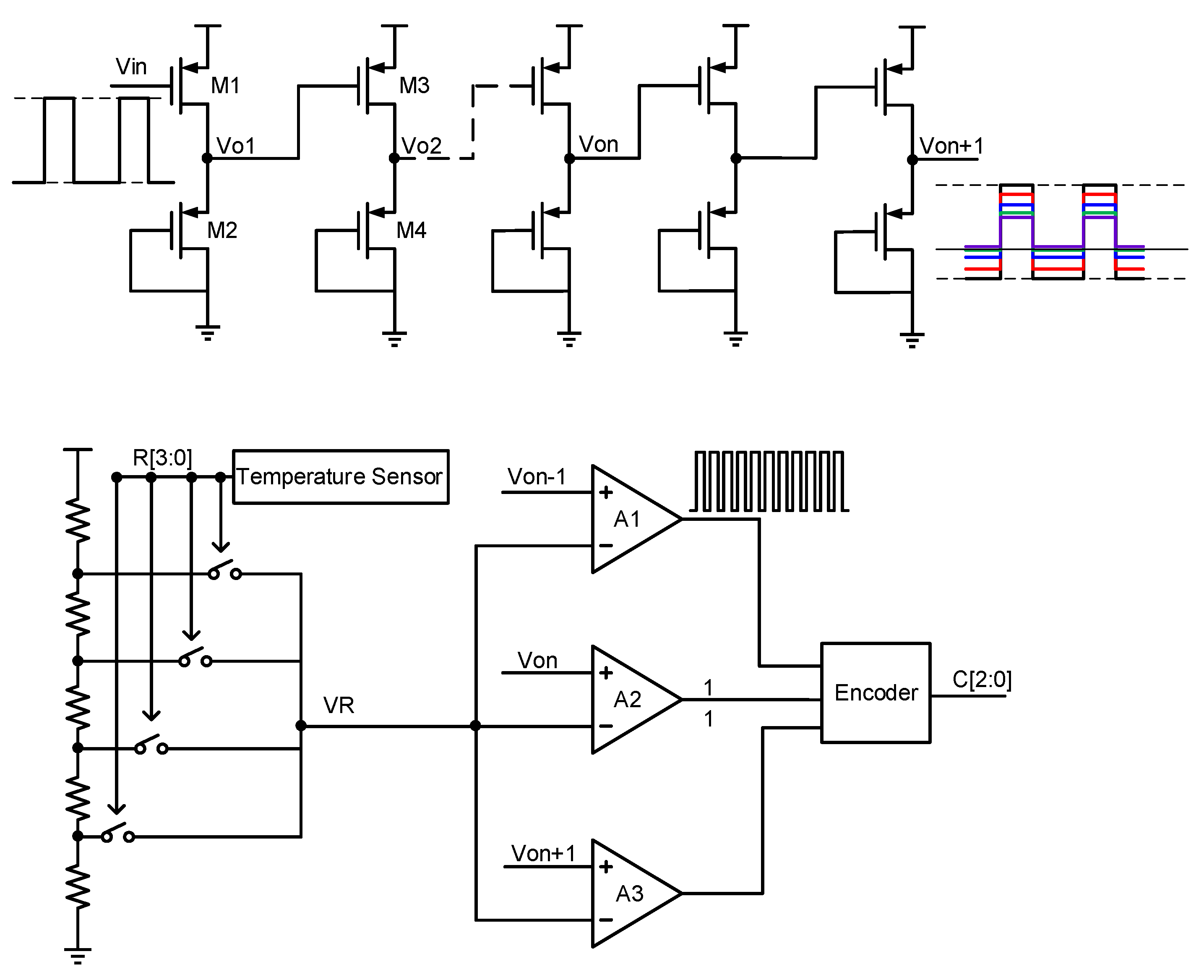
As shown in Figure 4, the process corner detection module comprises all P-transistors. The low level of the odd series increases with the increase in series, and there is always V n + 1 > V n > V n 1 at different process corners. When Vin is at a high level, M1 is not conductive, and M2 is always in the saturated region. Because V S G 2 | V T H | , it can be obtained:
V o 1 | V T H |
When Vin is at a low level, M1 is in the linear region, and M2 is in the saturated region. According to the principle of equal currents, it can be obtained:
1 2 μ p C o x W L ( V o 1 | V T H | ) 2 = μ p C o x W L [ ( V D D | V T H | ) ( V D D V o 1 ) 1 2 ( V D D V o 1 ) 2 ]
The output voltage Vo1 is obtained:
V o 1 = 1 2 ( V D D | V T H | ) + | V T H |
When Vo1 equals VTH, M3 is in the linear region, and M4 is in the saturated region. According to the principle of equal currents:
1 2 μ p C o x W L ( V o 2 | V T H | ) 2 = μ p C o x W L [ ( V D D 2 | V T H | ) ( V D D V o 2 ) 1 2 ( V D D V o 2 ) 2 ]
The output voltage Vo2 is obtained:
V o 2 = 6 | V T H | ± 2 9 V T H 2 8 | V T H | V D D + 2 V D D 2 4
When Vo1 is Equation (19), M3 is in the saturation region, and M4 is in the saturation region. The following equation can be obtained according to the principle of equal currents.
1 2 μ p C o x W L ( V o 2 | V T H | ) 2 = 1 2 μ p C o x W L ( V D D V o 1 | V T H | ) 2
The output voltage Vo2 is obtained:
V o 2 = 0.3 ( V D D | V T H | )
Comparing Equation (25) with 0, it can be seen that the low level of the odd series will increase with the increase in series.
Therefore, the output signals of the n 1 t h stage, the n t h stage, and the n + 1 t h stage are outputted to the three comparator circuits. As shown in Figure 5, different color pulse signals represent different odd-order outputs. At the same time, the reference voltage VR in different process corners is different so that the comparator can produce different output signals in different process corners. The three comparator circuits output a high level at the process corner ff. At the process corner tt, the comparator A1 outputs a pulse signal, and the comparators A2 and A3 output a high level. At the process corner ss, the comparators A1 and A2 output pulse signals, and the comparator A3 outputs a high level. These signals are transmitted to the coding module for coding. The coding module counts the rising edge of the input signal. To prevent false triggers and keep a certain margin, it outputs a low level when the number of the rising edge is larger than 7, and it outputs a high level when the number of the rising edge is less than 7. Then, which process corner the chip is currently at is judged. When the output signal C [2:0] of the coding module is 100, the corresponding process corner is ff. When it is 010, the corresponding process corner is tt. Moreover, when it is 001, the corresponding process corner is ss.
Because the circuit is inevitably affected by temperature and the influence of temperature is often more significant than that of the process corner, it could cause the overlapping phenomenon due to the influence of temperature in detecting the process corner. Therefore, it is necessary to conduct temperature-segmentation detection, as shown in Table 1. Different VRs are selected to compare in different temperature ranges. The output signal of the comparator is consistent at different process corners, and then different process corners can be distinguished in the temperature range of 135 °C to −40 °C.

4. Simulation and Experimental Results

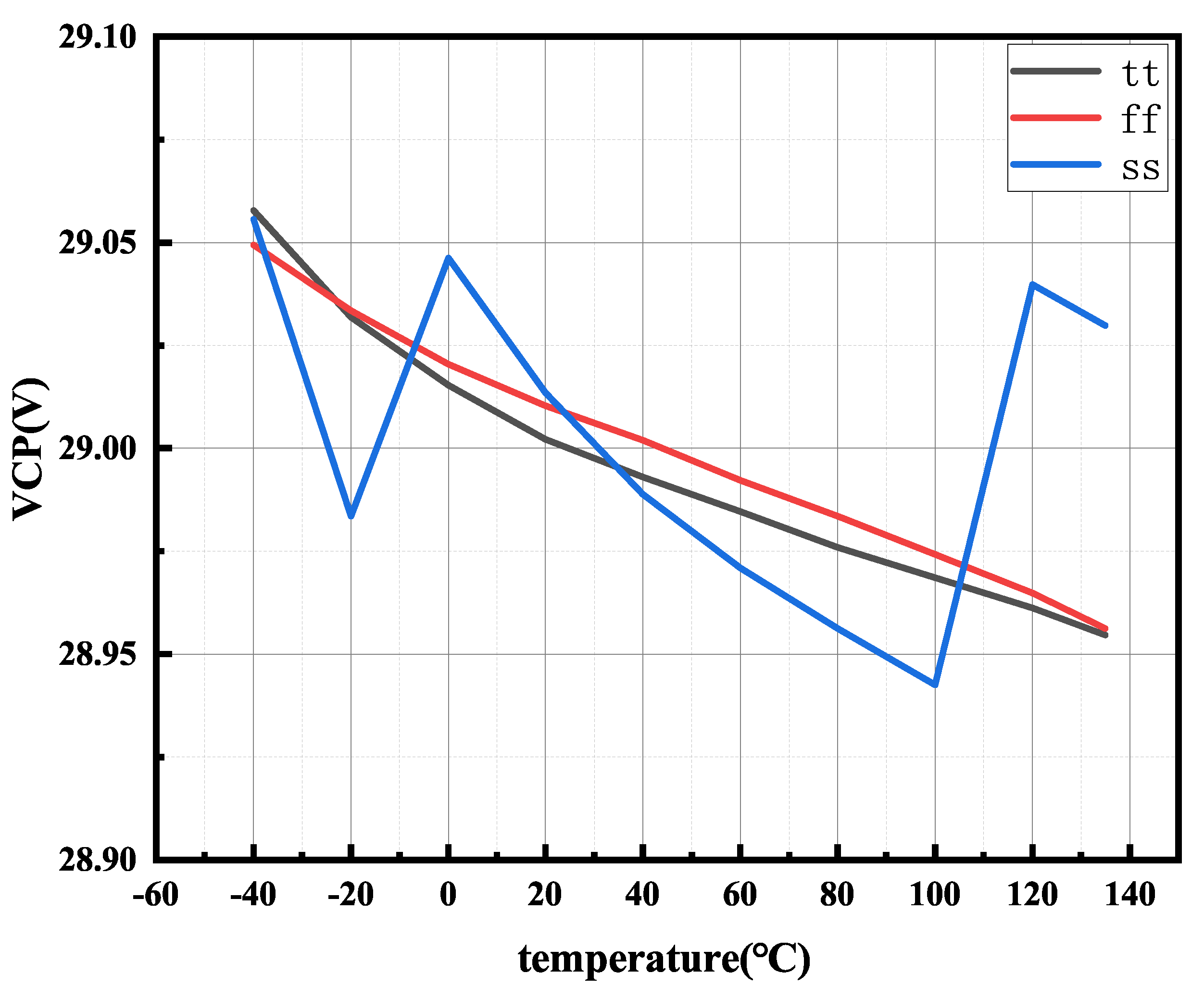
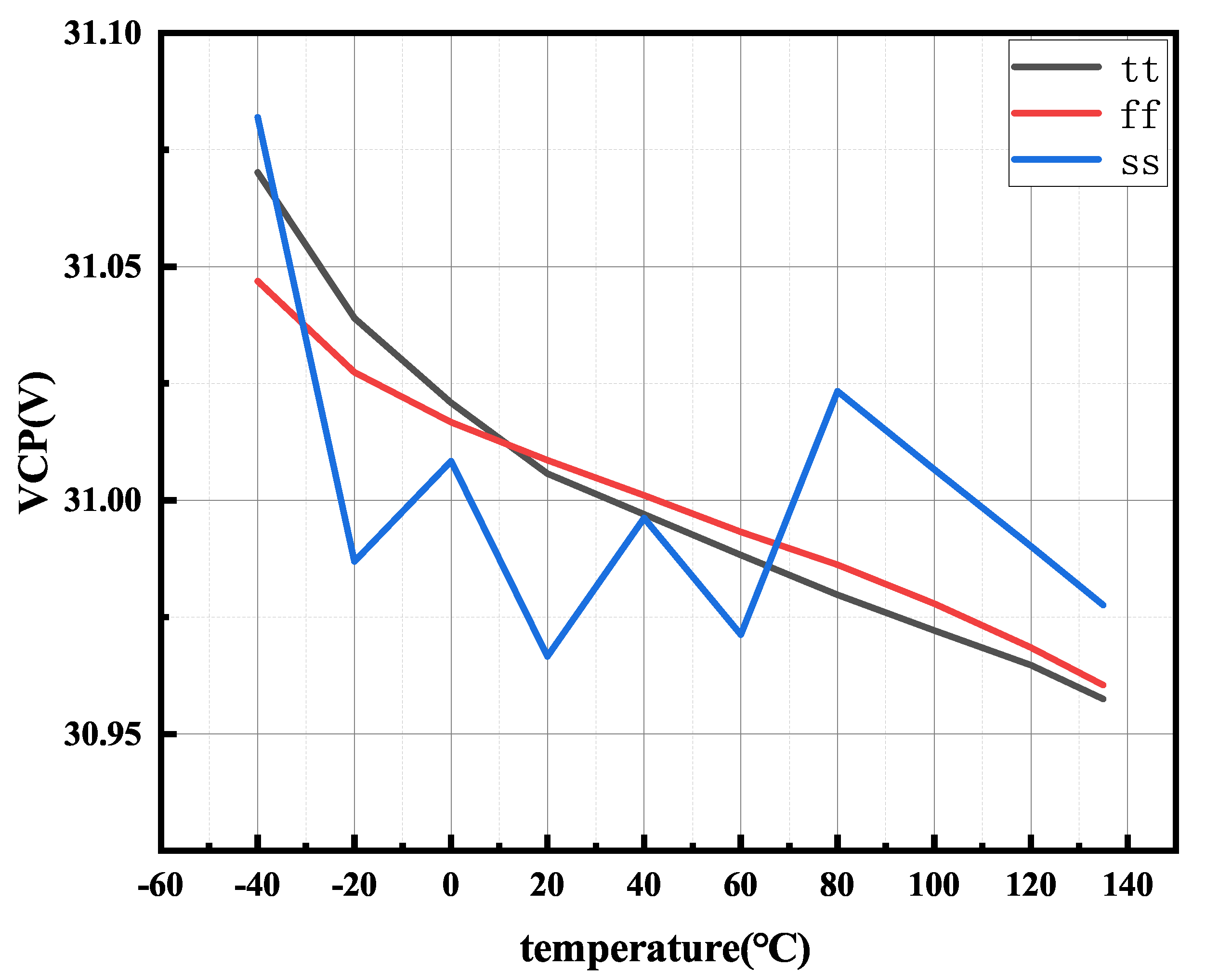
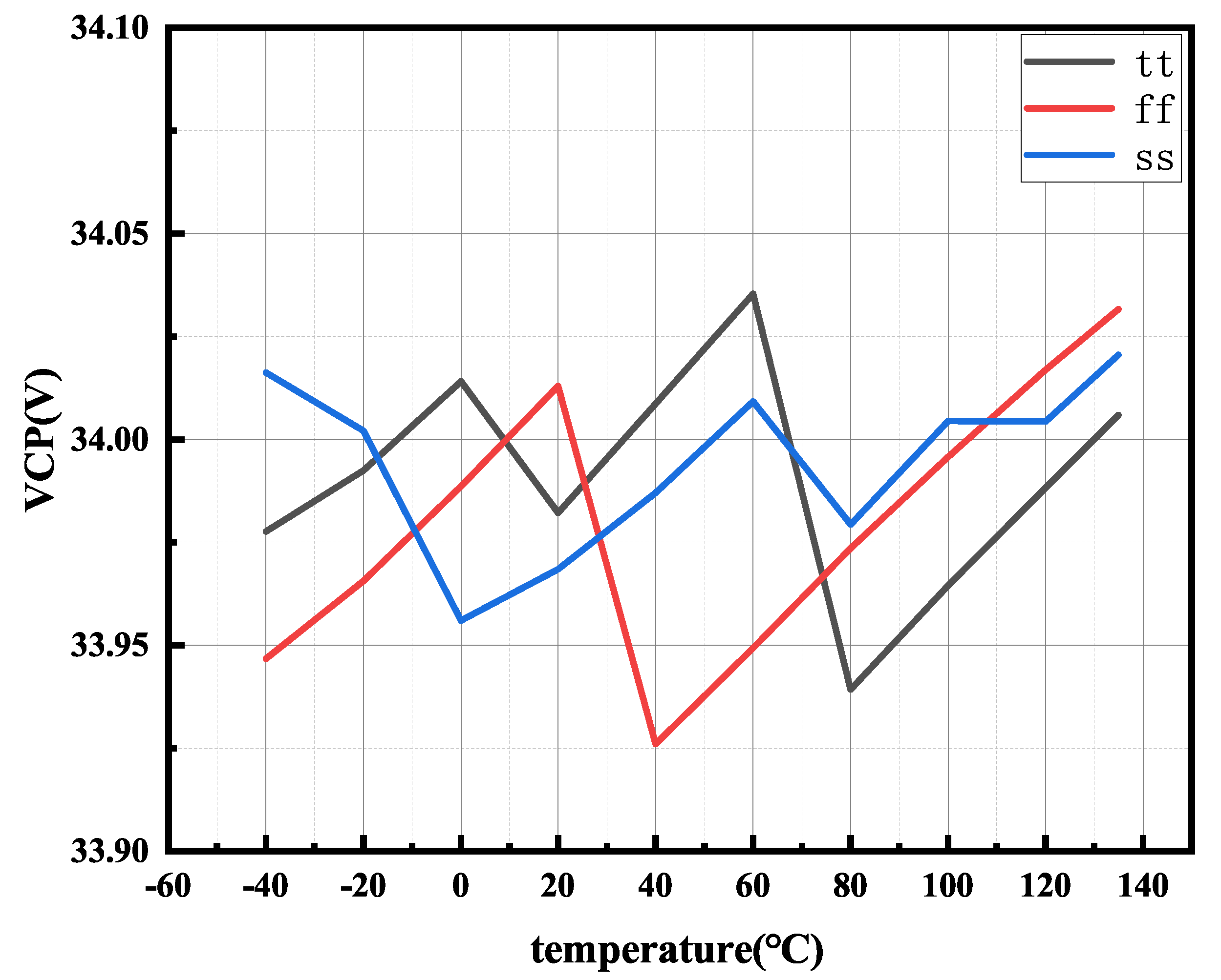
The proposed charge-pump circuit is fabricated in a 0.18 μ m CMOS process. The layout is shown in Figure 6, and the charge-pump circuit area is 880 μ m × 350 μ m. Figure 7 shows the output voltage at different corners when A1A2 = 00, VBB = 24 V, and temperature range is −40 °C to 135 °C. The output voltage can be stabilized at 29 V at different process corners and temperatures. Figure 8 and Figure 9 show the output voltage at different corners when A1A2 = 01 and A1A2 = 10. It can be seen that the output voltage values are 31 V and 34 V, respectively, and the maximum deviation can be measured to be ±0.265%. The specific deviation values are shown in Table 2.
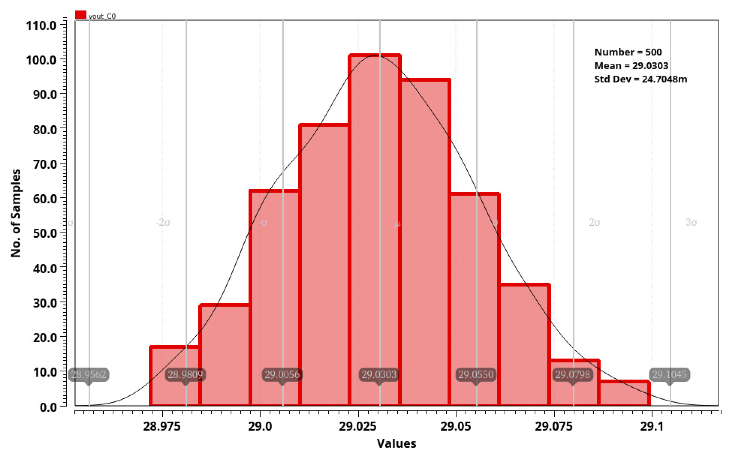
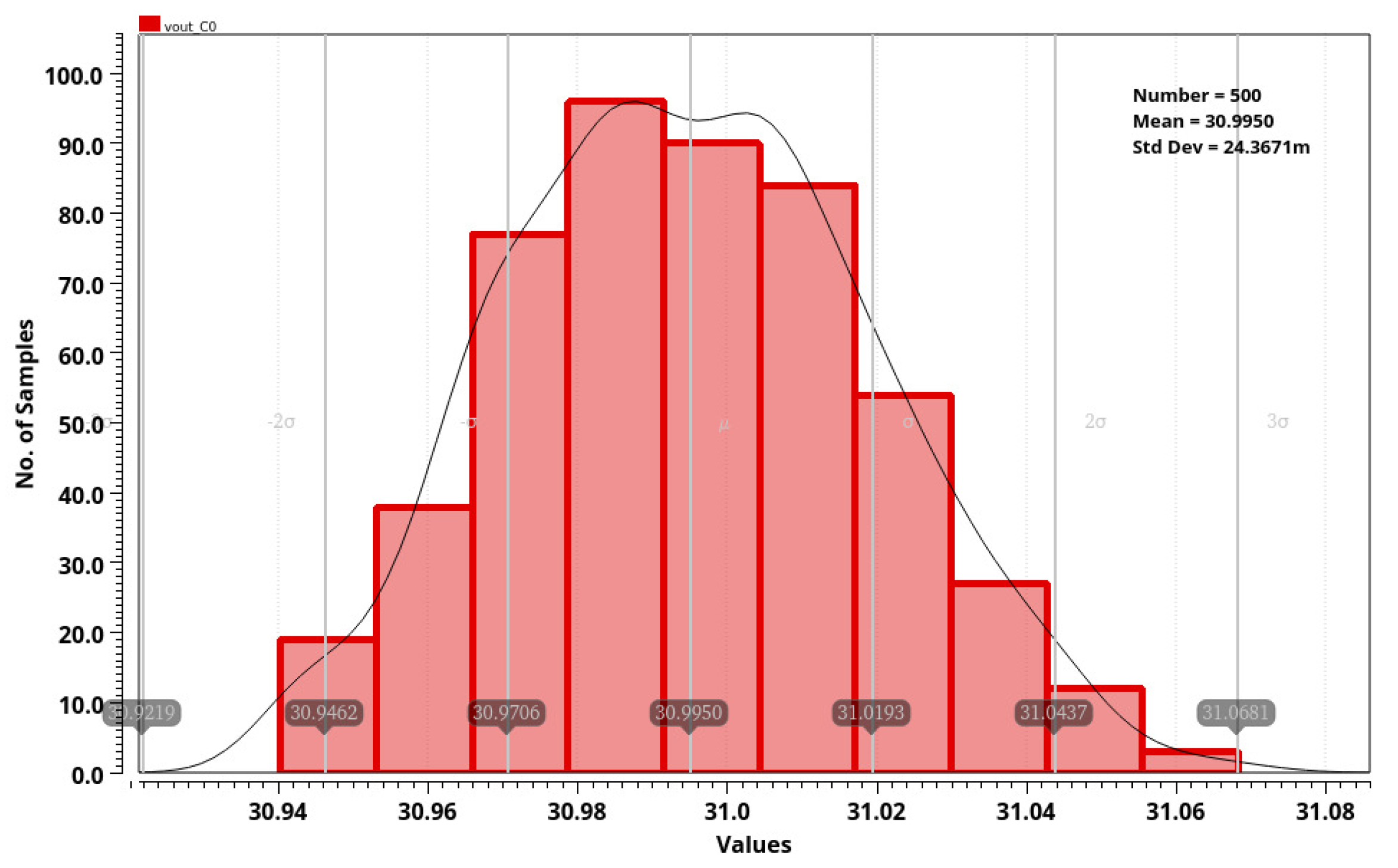
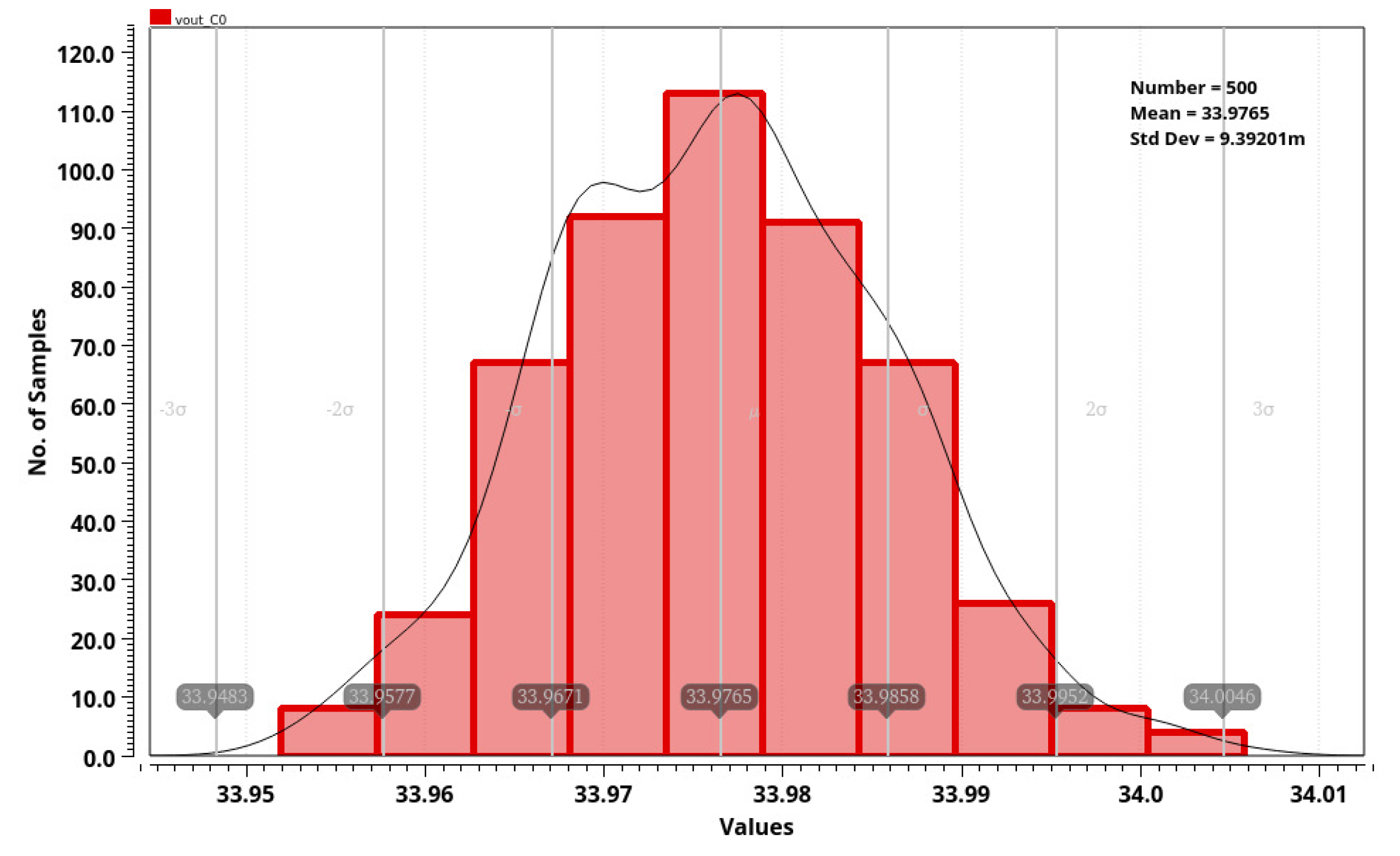
Figure 10, Figure 11 and Figure 12 show that a Monte Carlo simulation was carried out in 500 samples when VBB = 24 V, A1A2 = 00, A1A2 = 01, and A1A2 = 10 to evaluate the sensitivity of the output voltage under process variation and mismatch conditions. The worst case of the process sensitivity ( σ / μ ) is 0.1%. Here, σ represents a statistical term that reflects the size of the sample dispersion. In addition, μ represents the arithmetic mean of all the sample values. Again, it shows that the charge-pump structure designed in this paper has excellent performance, and the output voltage is stable and reliable.
Figure 13 shows the o variation of the output voltage when the VBB varies from 5 V to 32 V at the process corner tt and 27 °C. It can be seen that when the supply voltage fluctuates, the proposed circuit can still output a stable linear voltage signal.
Figure 14 shows the simulation results of the output voltage with the variation of the load current at different process corners and 27 °C when VBB = 24 V and A1A2 = 00. When the output is connected to different resistors, such as a resistor with a resistance value of 2.9 K, the load current flowing through the resistor is 10 mA. It can be seen that the maximum load current can reach 30 mA, and the output voltage remains stable at different process corners.
The proposed charge pump’s performance is summarized and compared with other charge pumps in Table 3. Although the process used in [20] is 0.16 μ m, the device parameters and process parameters are not much different between 0.16 μ m and 0.18 μ m, so they can be directly compared. Compared with the other circuits in the comparison table, our proposed circuit has a PVT-robust characteristic, so the ripple is less than 0.3%. At the same time, the output voltage can be adjusted, which can vary from 10 V to 42 V. The maximum load current is 30 mA, so the output driving capability is strong. Thus, it indicates that the proposed circuit has a wider output range, smaller ripple, and larger load current. In addition, it performs PVT robust.

5. Conclusions

This paper proposes a new charge-pump circuit, which can adjust its output voltage according to the working environment. Meanwhile, an on-chip compensation technology is proposed to make the circuit resistant to PVT variation. The proposed circuit is fabricated by a 180 nm BCD process. The difference between the output voltage of the charge pump and the power supply voltage is selected by signals A1 and A2, and the PVT compensation technology is adopted. The output voltage can remain stable at the supply voltage of 5–32 V, the temperature of −40 ℃ to 135 ℃, and different process corners. The output voltage can remain stable, and the maximum deviation is ±0.265%. The ripple is less than 0.3% ( Δ Vripple/Vout) when the maximum load current is 30 mA. Thus, the proposed circuit has a wider output range, smaller ripple, and larger load current. The charge-pump core area is 0.308 mm 2 , and the power consumption is 4.753 mW. The proposed circuit can be applied as a power supply module to supply power to different power transistors or loads.

Author Contributions

Conceptualization, X.M. and L.W.; methodology, X.M.; validation, L.W.; formal analysis, X.M.; investigation, X.M.; data curation, X.M.; writing—original draft preparation, X.M.; writing—review and editing, L.W. and J.Y.; project administration, L.W. All authors have read and agreed to the published version of the manuscript.

Funding

This research received no external funding.

Conflicts of Interest

The authors declare no conflict of interest.

References

  1. Singh, A.; Singh, T.; Pindoo, I.; Choudhary, A.; Kumar, R.; Bhullar, P. Transient response and dynamic power dissipation comparison of various Dickson charge pump configurations based on charge transfer switches. In Proceedings of the 2015 6th International Conference on Computing, Communication and Networking Technologies (ICCCNT), Dallas-Fortworth, TX, USA, 13–15 July 2015; pp. 1–6. [Google Scholar] [CrossRef]
  2. Chen, J.J.; Zheng, C.H.; Hwang, Y.S. A new single-inductor triple-output buck converter using CMOS technology. In Proceedings of the 2010 International Power Electronics Conference—ECCE ASIA, Sapporo, Japan, 21—24 June 2010; pp. 82–85. [Google Scholar] [CrossRef]
  3. Matsumoto, H.; Neba, Y.; Asahara, H. Variable-Form Carrier-Based PWM for Boost-Voltage Motor Driver with a Charge-Pump Circuit. IEEE Trans. Ind. Electron. 2015, 62, 4728–4738. [Google Scholar] [CrossRef]
  4. Wei, C.L.; Wu, C.H.; Wu, L.Y.; Shih, M.H. An Integrated Step-Up/Step-Down DC–DC Converter Implemented with Switched-Capacitor Circuits. IEEE Trans. Circuits Syst. II Express Briefs 2010, 57, 813–817. [Google Scholar] [CrossRef]
  5. Chen, M.; Wu, X.; Zhao, M. Novel high efficiency low ripple charge pump using variable frequency modulation. In Proceedings of the 2010 International Conference on Microelectronics, Cairo, Egypt, 19–22 December 2010; pp. 228–231. [Google Scholar] [CrossRef]
  6. Tan, Y.; Ishikuro, H. A Discrete-Time Model for Frequency Modulated Charge Pumps with Synchronized Controller. In Proceedings of the 2020 IEEE 63rd International Midwest Symposium on Circuits and Systems (MWSCAS), Springfield, MA, USA, 9–12 August 2020; pp. 929–932. [Google Scholar] [CrossRef]
  7. Huang, H.W.; Chen, K.H.; Kuo, S.Y. Dithering Skip Modulation, Width and Dead Time Controllers in Highly Efficient DC-DC Converters for System-On-Chip Applications. IEEE J. Solid-State Circuits 2007, 42, 2451–2465. [Google Scholar] [CrossRef]
  8. Wolpert, D.; Ampadu, P. A Low-Power Safety Mode for Variation Tolerant Systems-on-Chip. In Proceedings of the 2008 IEEE International Symposium on Defect and Fault Tolerance of VLSI Systems, Cambridge, MA, USA, 1–3 October 2008; pp. 33–41. [Google Scholar] [CrossRef]
  9. Chang, M.H.; Lin, S.Y.; Wu, P.C.; Zakoretska, O.; Chuang, C.T.; Chen, K.N.; Wang, C.C.; Chen, K.H.; Chiu, C.T.; Tong, H.M.; et al. Near-/Sub-Vth process, voltage, and temperature (PVT) sensors with dynamic voltage selection. In Proceedings of the 2013 IEEE International Symposium on Circuits and Systems (ISCAS), Beijing, China, 19–23 May 2013; pp. 133–136. [Google Scholar] [CrossRef]
  10. Huang, H.; Xu, H.; Elies, B.; Chiu, Y. A Non-Interleaved 12-b 330-MS/s Pipelined-SAR ADC with PVT-Stabilized Dynamic Amplifier Achieving Sub-1-dB SNDR Variation. IEEE J. Solid-State Circuits 2017, 52, 3235–3247. [Google Scholar] [CrossRef]
  11. Zhang, J.; Ren, X.; Liu, S.; Chan, C.H.; Zhu, Z. An 11-bit 100-MS/s Pipelined-SAR ADC Reusing PVT-Stabilized Dynamic Comparator in 65-nm CMOS. IEEE Trans. Circuits Syst. II Express Briefs 2020, 67, 1174–1178. [Google Scholar] [CrossRef]
  12. Chen, C.L.; Tseng, H.Y.; Kuo, R.C.; Wang, C.C. A slew rate self-adjusting 2 × VDD output buffer with PVT compensation. In Proceedings of the Technical Program of 2012 VLSI Design, Automation and Test, Hsinchu, Taiwan, 23–25 April 2012; pp. 1–4. [Google Scholar] [CrossRef]
  13. Giron-Allende, A.; Avendaño, V.; Martinez-Guerrero, E. A design methodology using flip-flops controlled by PVT variation detection. In Proceedings of the 2015 IEEE 6th Latin American Symposium on Circuits & Systems (LASCAS), Montevideo, Uruguay, 24–27 February 2015; pp. 1–4. [Google Scholar] [CrossRef]
  14. Kim, K.K.; Kim, Y.B. A Novel Adaptive Design Methodology for Minimum Leakage Power Considering PVT Variations on Nanoscale VLSI Systems. IEEE Trans. Very Large Scale Integr. (VLSI) Syst. 2009, 17, 517–528. [Google Scholar] [CrossRef]
  15. Wang, C.C.; Chao, K.Y.; Sampath, S.; Suresh, P. Anti-PVT-Variation Low-Power Time-to-Digital Converter Design Using 90-nm CMOS Process. IEEE Trans. Very Large Scale Integr. (VLSI) Syst. 2020, 28, 2069–2073. [Google Scholar] [CrossRef]
  16. Biswas, A.; Sinangil, Y.; Chandrakasan, A.P. A 28 nm FDSOI integrated reconfigurable switched-capacitor based step-up DC-DC converter with 88% peak efficiency. In Proceedings of the ESSCIRC 2014—40th European Solid State Circuits Conference (ESSCIRC), Venice Lido, Italy, 22–26 September 2014; pp. 271–274. [Google Scholar] [CrossRef]
  17. Hua, Z.; Lee, H. A Reconfigurable Dual-Output Switched-Capacitor DC-DC Regulator with Sub-Harmonic Adaptive-on-Time Control for Low-Power Applications. IEEE J. -Solid-State Circuits 2015, 50, 724–736. [Google Scholar] [CrossRef]
  18. Teh, C.K.; Suzuki, A. 12.3 A 2-output step-up/step-down switched-capacitor DC-DC converter with 95.8% peak efficiency and 0.85-to-3.6 V input voltage range. In Proceedings of the 2016 IEEE International Solid-State Circuits Conference (ISSCC), San Francisco, CA, USA, 31 January–4 February 2016; pp. 222–223. [Google Scholar] [CrossRef]
  19. Wei, C.L.; Shih, M.H. Design of a Switched-Capacitor DC-DC Converter with a Wide Input Voltage Range. IEEE Trans. Circuits Syst. I Regul. Pap. 2013, 60, 1648–1656. [Google Scholar] [CrossRef]
  20. Karadi, R.; Pique, G.V. 4.8 3-phase 6/1 switched-capacitor DC-DC boost converter providing 16 V at 7 mA and 70.3% efficiency in 1.1 mm3. In Proceedings of the 2014 IEEE International Solid-State Circuits Conference Digest of Technical Papers (ISSCC), San Francisco, CA, USA, 9–13 February 2014; pp. 92–93. [Google Scholar] [CrossRef]
  21. Yim, T.; Lee, C.; Yoon, H. A High Speed Modified Dickson Charge Pump. In Proceedings of the 2021 IEEE International Symposium on Circuits and Systems (ISCAS), Daegu, Korea, 22–28 May 2021; pp. 1–5. [Google Scholar] [CrossRef]
  22. Abdi, A.; Kim, H.S.; Cha, H.K. A High-Voltage Generation Charge-Pump IC Using Input Voltage Modulated Regulation for Neural Implant Devices. IEEE Trans. Circuits Syst. II Express Briefs 2019, 66, 342–346. [Google Scholar] [CrossRef]
  23. Zhao, J.; Yao, L.; Xue, R.F.; Li, P.; Je, M.; Xu, Y.P. An Integrated Wireless Power Management and Data Telemetry IC for High-Compliance-Voltage Electrical Stimulation Applications. IEEE Trans. Biomed. Circuits Syst. 2016, 10, 113–124. [Google Scholar] [CrossRef] [PubMed]
  24. Shen, B.; Bose, S.; Johnston, M.L. A 1.2 V–20 V Closed-Loop Charge Pump for High Dynamic Range Photodetector Array Biasing. IEEE Trans. Circuits Syst. II Express Briefs 2019, 66, 327–331. [Google Scholar] [CrossRef]
  25. Xie, Y.; Huang, S.; Xue, Y.; Duan, Q. A low-voltage with high pumping efficiency charge pump for flash memory. J. Phys. Conf. Ser. 2020, 1550, 052027. [Google Scholar] [CrossRef]
  26. Patil, A.; Bhat, S.; Santra, A. An Accurate, Power and Area Efficient 13.33x Charge Pump with Wide-Range Programmability for Biomedical Sensors. In Proceedings of the 2020 33rd International Conference on VLSI Design and 2020 19th International Conference on Embedded Systems (VLSID), Bangalore, India, 4–8 January 2020; pp. 219–224. [Google Scholar] [CrossRef]
  27. Li, X.; Li, R.; Ju, C.; Hou, B.; Zhang, R. A Regulated Temperature-Insensitive High-Voltage Charge Pump in Standard CMOS Process for Micromachined Gyroscopes. Sensors 2019, 19, 4149. [Google Scholar] [CrossRef] [Green Version]
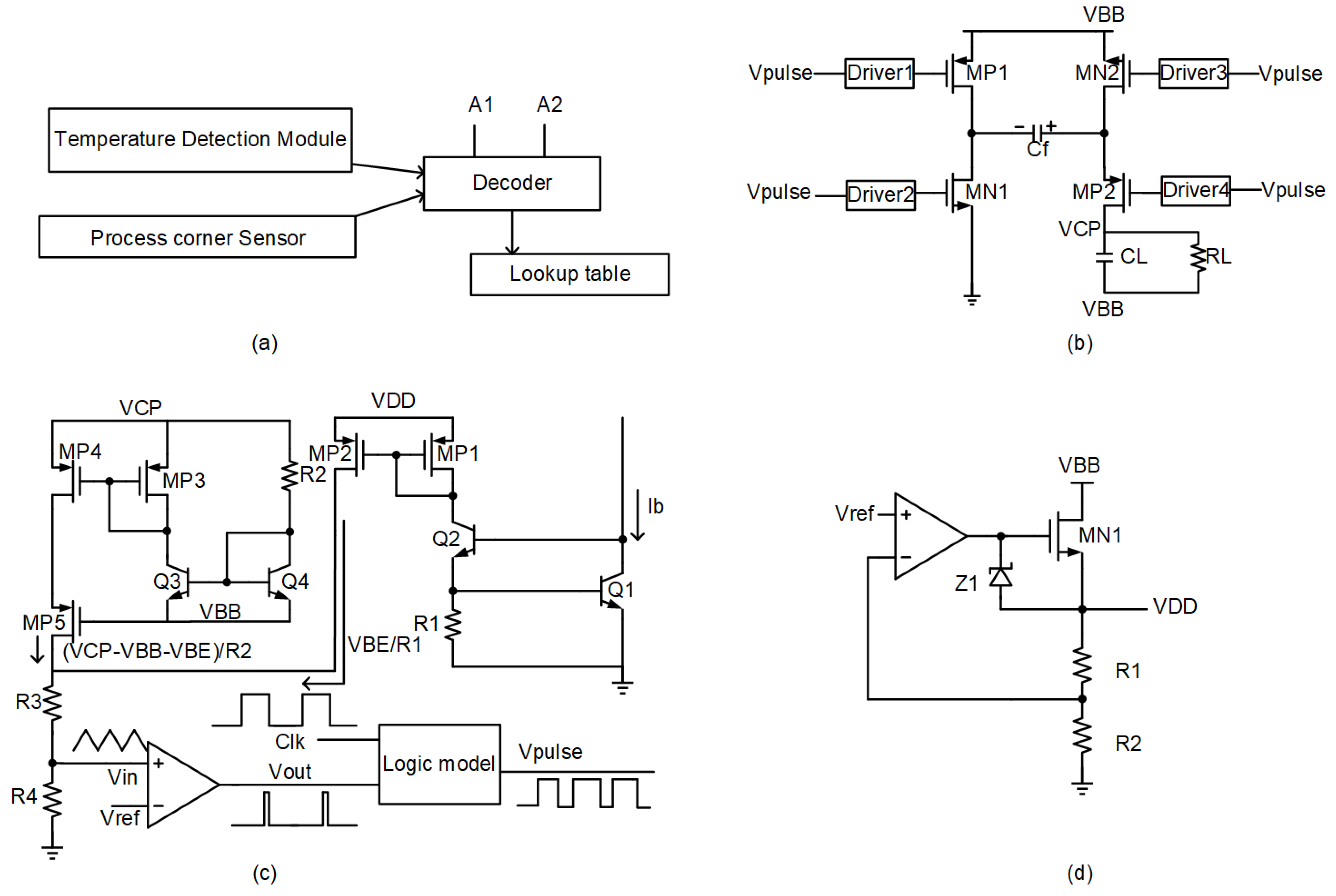
Figure 1. (a) Output voltage modulation module; (b) switched capacitor module; (c) PWM modulation module; and (d) high-voltage LDO module.
Electronics 11 02828 g001
Figure 2. Block diagram of switched capacitor module.
Electronics 11 02828 g002
Figure 3. Control Signal Timing Diagram.
Electronics 11 02828 g003
Figure 4. Process corner detection module.
Electronics 11 02828 g004
Figure 5. Three output modes of the encoder.
Electronics 11 02828 g005
Figure 6. The layout of the charge pump.
Electronics 11 02828 g006
Figure 7. Output voltage VCP when A1A2 = 00, VBB = 24 V.
Electronics 11 02828 g007
Figure 8. Output voltage VCP when A1A2 = 01, VBB = 24 V.
Electronics 11 02828 g008
Figure 9. Output voltage VCP when A1A2 = 10, VBB = 24 V.
Electronics 11 02828 g009
Figure 10. Monte Carlo simulation with A1A2 = 00, VBB = 24 V.
Electronics 11 02828 g010
Figure 11. Monte Carlo simulation with A1A2 = 01, VBB = 24 V.
Electronics 11 02828 g011
Figure 12. Monte Carlo simulation with A1A2 = 10, VBB = 24 V.
Electronics 11 02828 g012
Figure 13. Simulation results of the output signal when the supply voltage changes.
Electronics 11 02828 g013
Figure 14. Simulation results of the output signal when the supply voltage changes.
Electronics 11 02828 g014
Table 1. Temperature coding under different process corners.
R[3:0]00001000110011101111
ss135–110 °C105–75 °C70–40 °C35–−5 °C−10–−40 °C
tt135–110 °C105–80 °C75–45 °C40–−5 °C0–−40 °C
ff135–105 °C100–75 °C70–40 °C35–−5 °C0–−40 °C
Table 2. Deviation at different process corners.
Δ V (VCP-VBB)ssttff
5 V±0.197%±0.199%±0.170%
7 V±0.265%±0.226%±0.151%
10 V±0.129%±0.179%±0.218%
Table 3. The comparison results of the performance of circuits.
Reference[21][22][23][20][24][25][26][27]This Work
Input Voltage (V)1.22.84.63.33.31.21.855–32
Vout Voltage (V)7.0812.820165/19.66.1297.5–2413–16.9510–42
Output ripple ( Δ Vripple/Vout) 10.2%<1% @max.load<0.6% @max.load<1% @max.load-0.23%<1%<1.1%<0.3% @max.load
Compensation for PVT Variationsnonononononononoyes
Maximum loading current (mA)0.10.01–10.60.1–7-0.30.1-30
Frequency100 M10 K3 K–1 M6.67 M10/50 M100 M20 M10 K200 K
Flying capacitance-1 u1 u1 u----100 n
Load capacitance-1 u1 u100 n1 n-1 n-1 u
No. of Stages544161/115152Single
Power dissipation (mW)----3.56---4.753
Area (mm 2 )-0.6-1.650.063-0.0382.530.308
Technology0.18  μ m0.18  μ m0.18  μ m0.16  μ m0.18  μ m0.18  μ m0.18  μ mBCD0.18  μ m0.18  μ mBCD
ResultSimulatedMeasuredMeasuredMeasuredMeasuredSimulatedMeasuredMeasuredSimulated
1 Δ Vripple represents the output ripple voltage and Vout represents the output signal value of the charge pump.
Publisher’s Note: MDPI stays neutral with regard to jurisdictional claims in published maps and institutional affiliations.